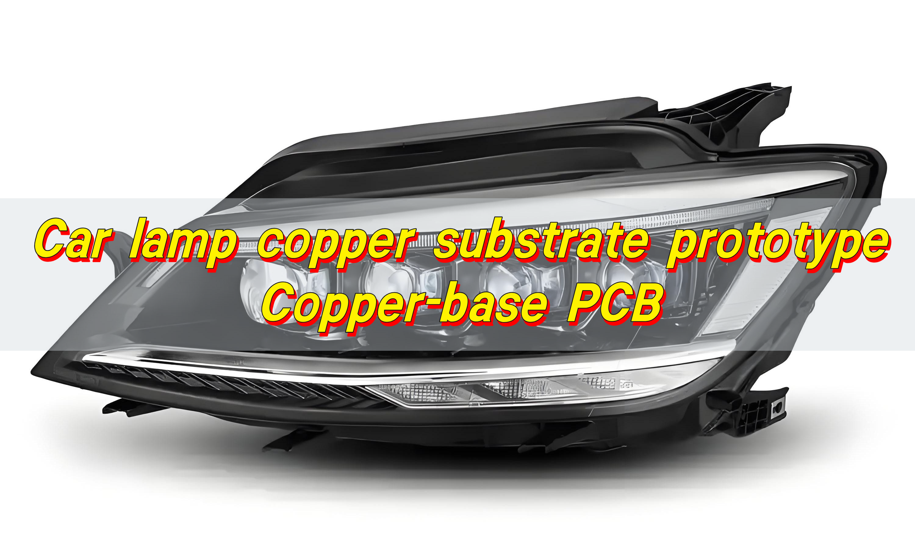
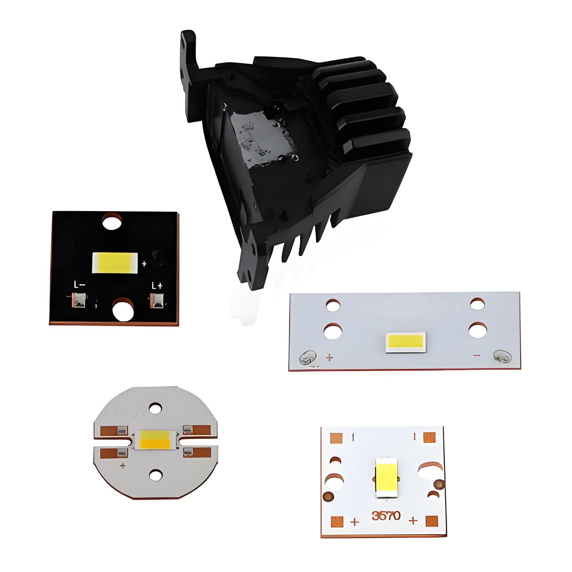
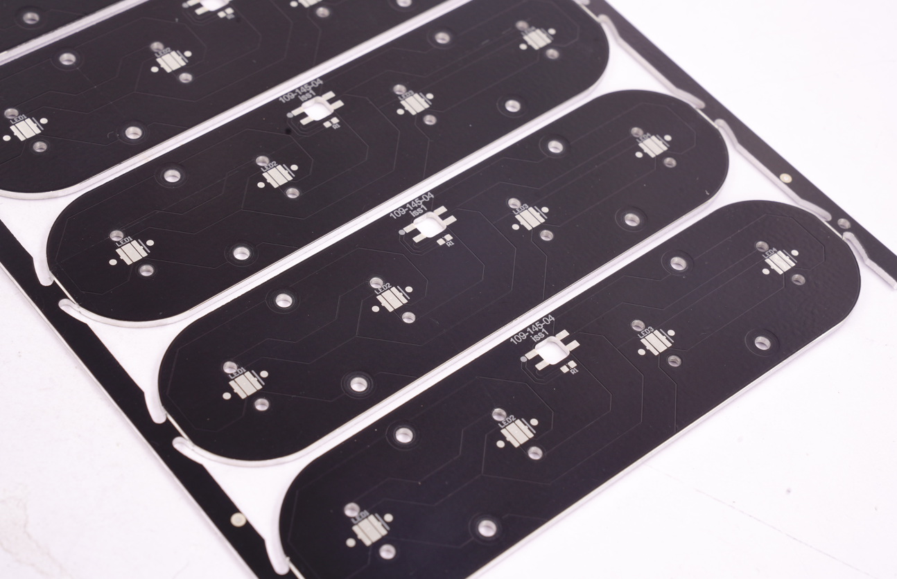
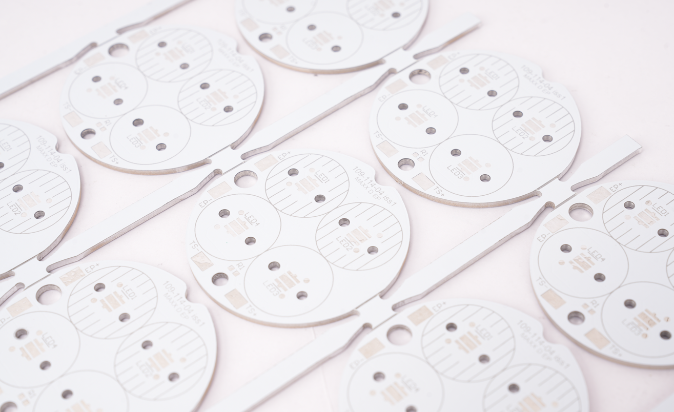
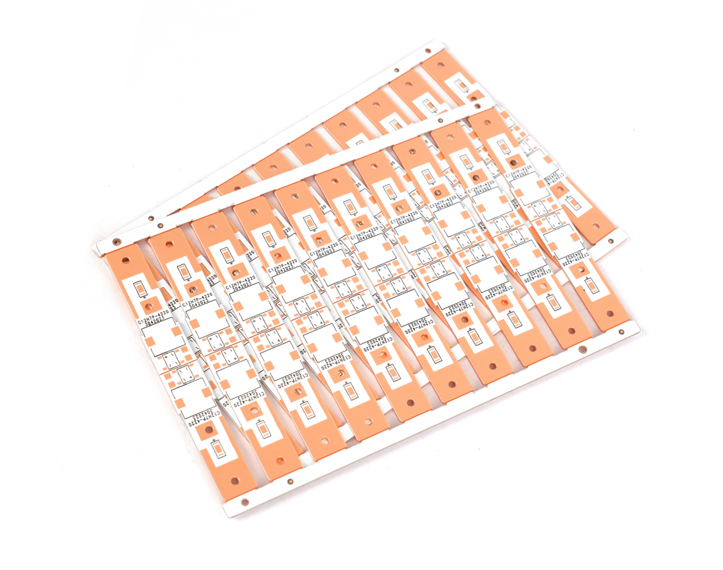
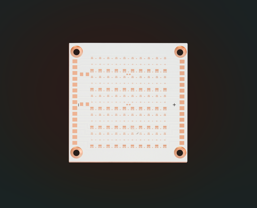
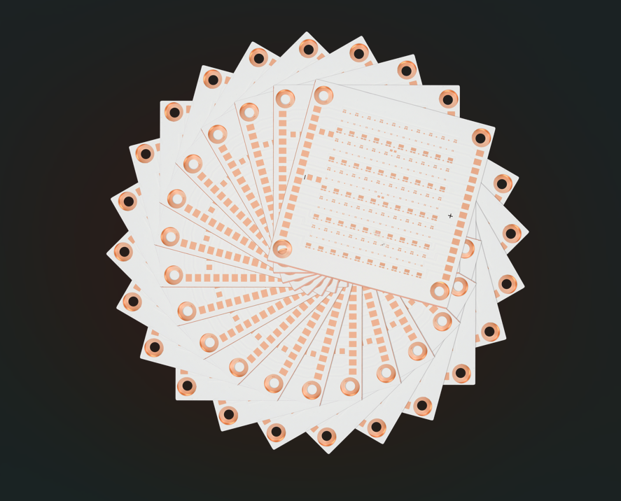
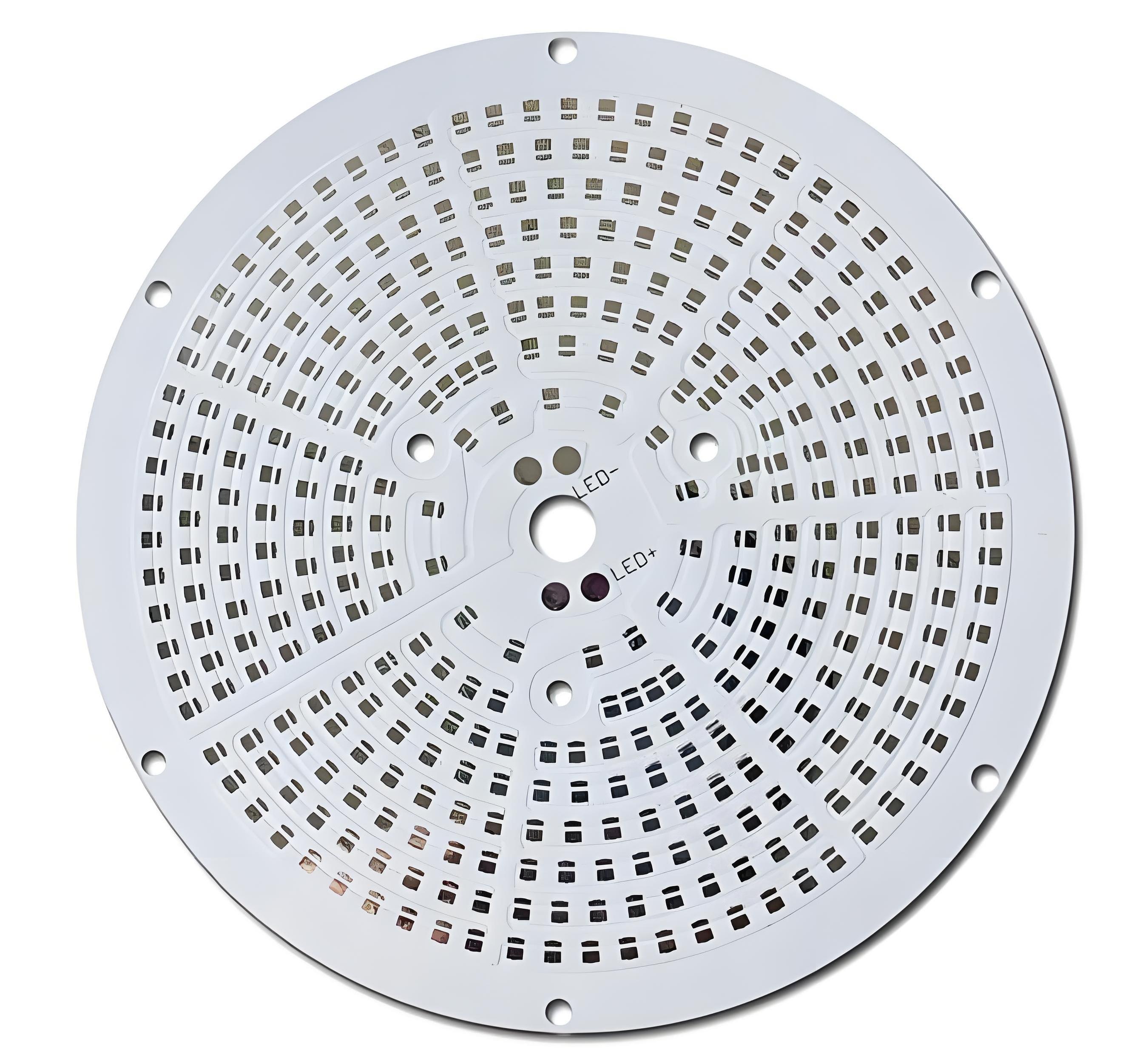
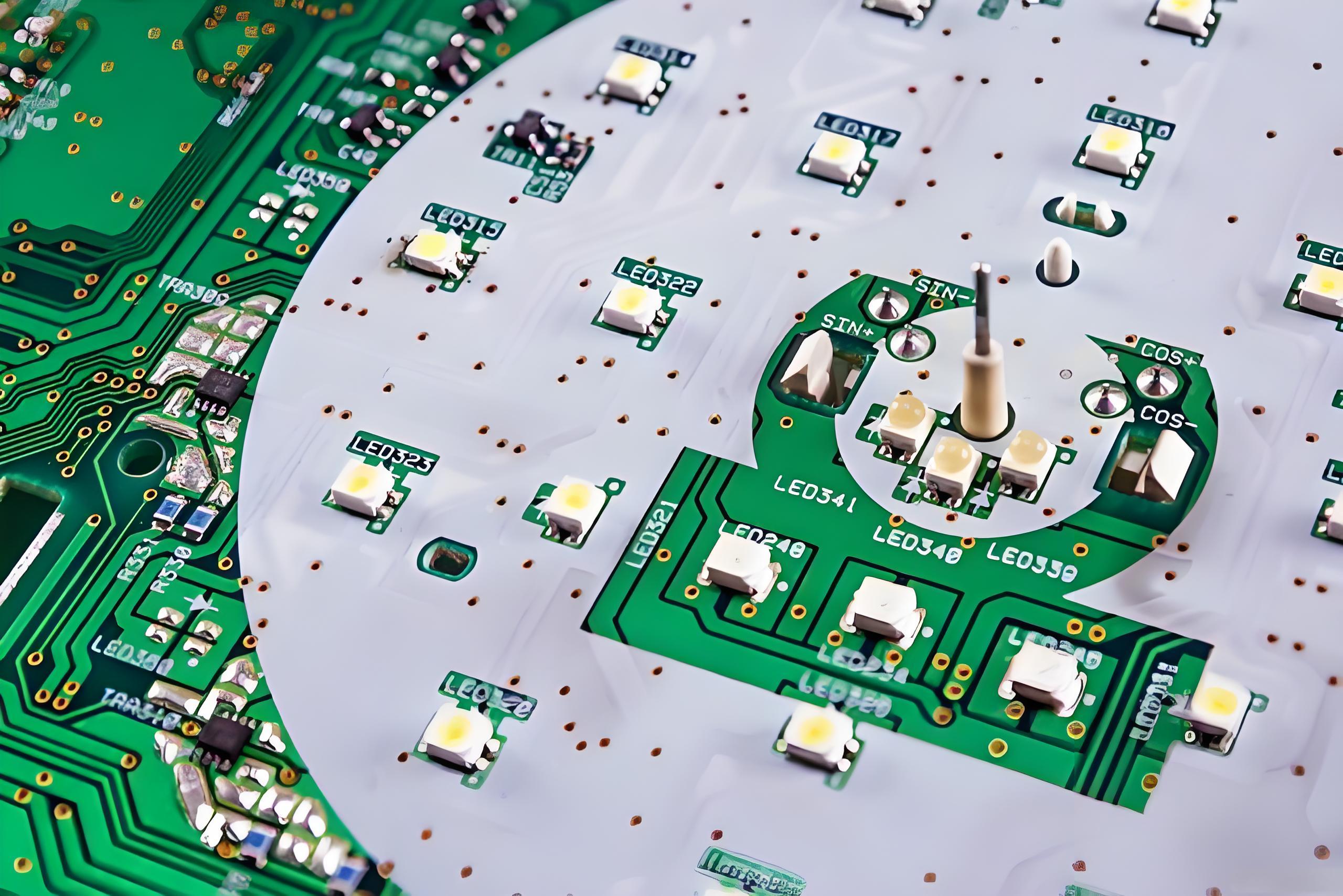
Car lamp copper substrate prototype is a sample board designed to test lighting performance in automotive lamps before full production. It uses a copper base to improve heat dissipation, conductivity, and reliability. In modern vehicles, precision and efficiency are crucial, and prototypes allow you to fine-tune the brightness, structure, and safety of LEDs before mass production.
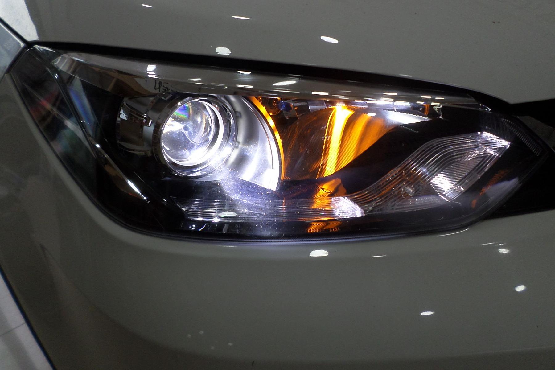
These copper-based PCBs act as the foundation beneath LED chips in headlamps, tail lights, fog lights, and interior lighting. They allow the design team to validate performance before mass production. That’s why they play a key role in making sure your headlights don’t just look great but also work flawlessly under harsh road conditions.
How does a car lamp prototype use copper substrate?
The prototype integrates copper substrates as the main heat management layer. LEDs generate a lot of heat in a compact space. Copper’s excellent thermal conductivity solves this issue. It transfers heat away from the LED and into a heat sink or surrounding structure.
Also, copper offers superior strength and rigidity compared to aluminum or fiberglass.
How does copper improve car lamps?
Copper elevates the entire performance of car lamps. Let’s look at how:
Better Thermal Performance: Copper can handle temperatures up to 300°C.
More Reliable Connections: Solder joints stay intact, even under constant on/off cycles.
Higher Brightness: Stable temperature means you can push the LEDs harder, which results in brighter light output.
Faster Response: Copper’s conductivity helps LEDs respond instantly when switched on.
Longer Lifespan: Better heat control extends the life of LEDs by thousands of hours.
When you combine these benefits, it doesn’t just make the lamps look better—it makes them last longer and work more reliably.
Why use copper in car lamp LEDs?
There are many reasons copper is favored in LED-based car lamps:
Heat Management: As LEDs run, heat builds up fast. Copper gets rid of that heat quickly.
Smaller Design, Stronger Output: Copper allows for a compact lamp body without sacrificing light power.
Energy Efficiency: Less heat loss means more electrical energy turns into light, not wasted warmth.
EMI Shielding: Copper can also help reduce electromagnetic interference, important for smart vehicles with many electronic systems.
Are copper substrates better for car lamp heat control?
Yes—without question.
Heat control is where copper wins by a wide margin. It transfers heat 8–10 times faster than standard FR4 or aluminum-core substrates. This matters in high-performance LED applications like car lamps, where even small temperature rises can cause damage.
For example, a typical LED PCB made from FR4 might start failing after a few months of hard use. A copper PCB under the same load? It can keep going strong for years.
The reason is simple: copper substrates allow for lower thermal resistance. That means heat leaves the LED zone faster and keeps the board cool.
In stop-and-go traffic, under direct sun, or during long nighttime drives, that’s the kind of performance you need from your lighting system.
What makes a copper substrate ideal for car lamps?
Several characteristics make copper substrates a top pick:
High Thermal Conductivity: Up to 400W/m·K. This number is unmatched in PCB materials.
Stability Over Time: Copper doesn’t warp, degrade, or oxidize easily.
Customization Flexibility: It can be etched, layered, and patterned for any LED layout.
Strength: Copper plates offer mechanical support for both the LEDs and the housing.
Compact Integration: You can fit more features into a smaller space.
If you’re building headlights with sharp beam angles, complex arrays, or adaptive functions, these benefits make copper unbeatable. The prototype phase becomes more precise, more flexible, and more representative of the final product.
Does copper boost car lamp LED lifespan?
Yes, significantly. LEDs degrade mostly due to heat. The hotter they run, the shorter their lifespan. Copper substrates cut that risk dramatically.
When used in a prototype, they help simulate real-world usage. Engineers can test things like:
Duty cycles
Temperature ranges
Load stress
Humidity and vibration
If the copper handles it well in tests, chances are the final product will hold up even better. In many studies, copper substrate boards extended LED lifespan by 25% to 60%, depending on the design and application. That’s not just a technical benefit—it’s a big cost saver too.
How to choose a car substrate for copper LED lamps?
Choosing the right substrate depends on your project goals. Here’s a breakdown:
LED Type and Power Output: High-lumen LEDs need thicker copper layers (2oz or more).
Size and Shape of the Lamp Housing: Custom-cut copper cores can be used to match exact dimensions.
Thermal Performance Needs: If your design will run hot, go with a thicker or multi-layer copper PCB.
Environmental Conditions: For harsh climates, use a treated copper layer to resist corrosion.
Mounting Type: If you use SMT, make sure your copper substrate has tight tolerances.
Cost Efficiency: Balance copper thickness with board size to keep costs manageable.
At EBest Circuit (Best Technology), we help you choose the best copper substrate based on both engineering specs and business needs. Whether you need a small run for testing or a large batch for production, we can tailor the solution.
Conclusion:
Copper substrate prototypes are a game-changer for car lamp development. They offer superior thermal control, better conductivity, and unmatched durability.
If you’re planning a new lighting system or want to improve an existing design, consider using a car lamp copper substrate prototype.
For expert advice, customized designs, or a quote on your copper-base PCB needs, feel free to contact us at sales@bestpcbs.com
What is 12v MCPCB? Let’s discover its features, applications, benefits, design guide, production process and how to get a quote for 12v MCPCB.
Are you worried about these issues?
Is your LED lamp’s lifespan frequently declining due to high temperatures? How can traditional PCBs overcome the thermal resistance bottleneck?
In high-power 12V applications, are copper foil erosion and voltage drop issues significantly compromising your product’s stability?
Can the supply chain provide a cost-effective solution while ensuring industrial-grade reliability and controlling BOM costs?
EBest Circuit (Best Technology) can provide solutions:
Metal substrate + nano-thermal conductive layer: Using a 1.5mm aluminum substrate and a ceramic composite dielectric, thermal resistance is reduced by 40%, ensuring LED junction temperature ≤85°C.
4oz thick copper + laser micro-hole technology: Supports 20A continuous current, avoids local overheating through design-for-manufacturing optimization, and maintains voltage fluctuations below 3%.
Vertically integrated supply chain: From substrate to SMT, we manufacture the entire process in-house, reducing mass production costs by 30% and enabling fast delivery of small batches (starting in 7 days).
With 19 years of experience in metal substrates, we are not just a supplier, but your thermal management partner for high-reliability LED solutions. Contact us now if you have any request for 12v MCPCB: sales@bestpcbs.com.
What Is a 12V MCPCB?
A 12V MCPCB(Metal Core Printed Circuit Board) is a specialized PCB using a metal substrate (e.g., aluminum or copper) as its core for efficient heat dissipation, designed to operate under 12-volt direct current (DC) systems. Its metal base layer rapidly conducts heat away from components, ensuring thermal stability and reliability. A 12V LED MCPCB specifically integrates this structure to support LED devices, combining 12V power compatibility with optimized thermal management for high-brightness or high-power LED applications.
What Are Features of 12V MCPCB?
Voltage-Specific Design: Optimized for 12V DC systems, with trace widths and copper thicknesses (e.g., 2–3 oz) tailored to handle high current at low voltage.
Enhanced Thermal Performance: Metal core (aluminum/copper) substrate with high thermal conductivity (2–38 W/m·K) rapidly dissipates heat, preventing thermal runaway in 12V power circuits.
Thick Copper Traces: Heavy copper layers (≥2 oz) reduce resistive losses, enabling efficient current delivery for 12V LED drivers, motors, or power modules.
Dielectric Insulation Layer: Specialized insulating material (e.g., epoxy-filled fiberglass) between metal core and copper traces ensures electrical isolation (≥500V breakdown voltage).
Compact Layer Stackup: Typically 2-layer structure (signal + metal core) simplifies design for space-constrained 12V applications while maintaining mechanical rigidity.
Thermal Stress Resistance: Metal substrate minimizes warping under thermal cycling, critical for 12V devices exposed to repeated heating/cooling (e.g., automotive LEDs).
High-Current Trace Routing: Wide traces or copper pours accommodate 12V high-current paths (e.g., >5A) without excessive temperature rise.
What Are Applications of 12V MCPCB?
LED Lighting Systems – Used in 12V LED strips, downlights, and streetlights, where metal-core PCBs efficiently dissipate heat from high-brightness LEDs, ensuring long lifespan and stable output.
Automotive Electronics – Applied in 12V vehicle components (e.g., dashboard backlighting, interior/exterior LED lights, sensors) for vibration resistance and thermal management in harsh automotive environments.
Power Conversion Modules – Integrated into 12V DC-DC converters, adapters, or battery chargers to handle high current with minimal heat buildup, enhancing reliability and efficiency.
Industrial Control Equipment – Used in 12V motor drivers, PLC (Programmable Logic Controller) modules, or automation systems requiring compact, thermally robust PCBs for stable operation.
Consumer Electronics Accessories – Found in 12V portable devices (e.g., power banks, USB hubs) to manage heat from power delivery components while maintaining compact form factors.
Solar-Powered Lighting – Deployed in 12V solar streetlights or garden lamps, where MCPCBs ensure efficient heat dissipation for LEDs powered by solar batteries, improving system durability.
Superior Thermal Management: The aluminum/copper core rapidly dissipates heat, preventing LED performance degradation and extending lifespan.
High Current Stability: Thick copper traces (35–280μm) ensure stable 12V power delivery, reducing voltage drops in high-power LED circuits.
Enhanced Durability: Resists thermal cycling and mechanical stress, ideal for outdoor LED lighting and harsh environments.
Energy Efficiency: Low thermal resistance minimizes energy loss, improving LED efficiency and reducing cooling costs.
Compact Design: Enables slimmer LED modules compared to traditional PCBs, suitable for space-constrained applications.
Long-Term Reliability: Prevents delamination and solder joint failures, ensuring consistent 12V LED performance over time.
Customizable Solutions: Supports multi-layer designs and flexible shapes for diverse high-power LED configurations.
Cost-Effective Maintenance: Reduces LED failure rates, lowering replacement and servicing costs in commercial/industrial setups.
How to Design A 12V MCPCB for High Power LED?
12V MCPCB Design Guide for High-Power LEDs
1. Define Requirements
Confirm LED specifications (voltage, current, thermal resistance).
Determine PCB dimensions and mounting method (e.g., heat sink compatibility).
2. Material Selection
Choose aluminum-core substrate (1.5mm–3.2mm thickness) for heat dissipation.
Use 2oz–4oz copper for traces to handle high currents.
Select a dielectric layer (polyimide or ceramic-filled epoxy) rated for ≥12V.
3. Circuit Layout
Arrange LEDs in series to match 12V input.
Design wide traces (≥2mm for 5A–10A) and minimize sharp bends.
Place thermal vias (0.3mm–0.5mm diameter) beneath LED pads to conduct heat to the aluminum base.
4. Thermal Design
Add a copper pour layer on the bottom PCB side, connected to thermal vias.
Ensure dielectric layer thickness (50µm–100µm) balances insulation and heat transfer.
Plan mounting holes for external heat sinks; use thermal interface material (TIM) between PCB and sink.
5. Manufacturing Preparation
Apply solder mask to protect copper traces.
Specify high-temperature solder (e.g., SAC305) for LED assembly.
Maintain ≥0.2mm trace-to-trace clearance and ≥1mm dielectric edge margin.
6. Validation
Test thermal performance using infrared imaging under maximum load (aim for ≤5°C rise above ambient).
Verify voltage stability and trace current capacity.
Run accelerated aging tests (e.g., 1000 hours at 85°C) to confirm long-term reliability.
7. Considerations
Avoid overcrowding LEDs to prevent localized heating.
Ensure thermal vias are evenly distributed under high-power components.
Validate dielectric material compatibility with operating temperatures.
Use PCB design tools (e.g., Altium, Eagle) for layout accuracy.
Partner with manufacturers experienced in MCPCB fabrication for quality control.
How to Make A 12V LED MCPCB?
Production Process for 12V LED MCPCB
1. Material Preparation: Cut aluminum substrate (e.g., 5052/6061 series) to required dimensions. Clean surfaces to remove oils and impurities.
2. Drilling: Use CNC drills to create via holes and mounting holes. Ensure precision (e.g., ±50µm tolerance).
3. Dry Film Imaging & Etching: Apply dry film photoresist, expose to UV light through circuit patterns, and develop to retain copper traces. Chemically etch away excess copper, leaving only the designed circuitry.
4. Insulating Layer Deposition: Coat the aluminum base with a dielectric material (e.g., epoxy resin or ceramic-filled polymer) via screen printing.
5. Metallization: Deposit copper layers (1oz–4oz) on the insulating layer using electroplating or chemical sinking.
6. Surface Finish: Apply surface treatments like HASL (spray tin), ENIG (immersion gold), or OSP (organic solderability preservative) for solderability.
7. Component Assembly: Use SMT (Surface Mount Technology) to place LEDs, resistors, and other components. Reflow solder in a controlled oven.
8. Testing & Inspection: Perform electrical tests (continuity, voltage drop) and thermal imaging (≤5°C rise above ambient). Conduct AOI (Automated Optical Inspection) for defects like shorts or misalignment.
9. Packaging: Vacuum-seal finished boards with desiccant packs. Include test reports and label specifications.
Why Choose EBest Circuit (Best Technology) as LED MCPCB Manufacturer?
19+ Years Industry Experience: Leverages proven expertise to navigate complex high power LED applications.
Stringent Quality Certifications (ISO9001, ISO13485, and IATF16949): Ensures product consistency and compliance with global standards.
Advanced Thermal Management Solutions: Prevents LED overheating, extending product lifespan and reliability.
Competitive Pricing: No Hidden Cost. Affordable pricing without compromising quality, ideal for cost-sensitive projects.
24 Hours Rapid Prototyping: Accelerates time-to-market, meeting urgent production demands.
Free DFM (Design for Manufacturability) Service: Identifies design flaws early, reducing rework costs and delays.
Advanced Quality Control – 100% automated optical inspection (AOI) and X-ray testing for defect-free boards.
Reliable Supply Chain – Stable material sourcing to avoid delays and ensure consistency.
One-Stop Solution – From prototyping to mass production, we handle all stages seamlessly.
Dedicated Customer Service – 24/7 technical support for real-time project tracking and issue resolution.
How to Get A Quote For LED MCPCB Project?
Essential Information for Accurate Quotation
1. Design Files:
Gerber/ODB++ files, Bill of Materials (BOM), and 3D mechanical drawings.
2. Technical Specs:
LED type (e.g., Cree XP-G3, Samsung LH351H) and power rating.
Circuit voltage (12V/24V) and current requirements.
How to choose copper etching PCB solution? A guide to selecting optimal copper PCB etching solutions: methods, tolerances, and process specifications.
Are you troubled with these issues?
When high-frequency devices are running, can your copper substrate quickly dissipate heat to avoid performance degradation?
With traditional processes, do material waste and yield fluctuations leave you struggling to manage costs?
When orders suddenly surge, can your supplier respond and deliver reliably within 72 hours?
EBest Circuit (Best Technology) can provide services and solutions:
Gradient Heat Dissipation Structure: Using nano-scale copper lamination technology, thermal resistance is reduced by 40%, ensuring long-term stable operation in high-temperature environments.
Lean Production System: Utilizing a closed-loop quality monitoring system, material utilization has increased to 92%, reducing unit costs by 15%.
Flexible Supply Chain Network: Three factories across China collaborate, enabling 7-day delivery for regular orders and lightning-fast scheduling for expedited orders.
Welcome to contact us if you have any request for metal core PCB: sales@bestpcbs.com.
What is Copper PCB Etching?
Copper PCB etching is a critical manufacturing process that selectively removes unwanted copper from a copper-clad printed circuit board (PCB) to create precise circuit patterns. By chemically dissolving unprotected copper areas while preserving resist-coated traces, this technique transforms raw copper-clad substrates into functional electronic components. The process involves two main approaches: acidic etching (using ferric chloride or cupric chloride solutions) for cost-effective mass production, and alkaline etching (with ammonia-based solutions) for high-precision applications requiring minimal side etching. Copper-clad PCB etching must balance speed, precision, and environmental considerations to achieve optimal results in electronic fabrication.
Large-Scale Production: Prioritize for alkaline copper chloride etchants. They offer the fastest etching speed (2.0–2.5 mil/min) and a high etch factor (4:1), ideal for high-throughput scenarios and thick copper layers.
Small-Scale/Hobbyist Use: Choose sulfuric acid–hydrogen peroxide solutions. They are cost-effective (1/3 the cost of ferric chloride), eco-friendly (produce only copper sulfate waste), and support copper recovery for sustainability.
MCPCB Type Compatibility
Inner Layer Boards: Use acidic copper chloride etchants. Their simple chemistry and wide parameter window ensure stable performance with minimal maintenance, suitable for stable inner-layer processes.
Outer Layer Boards: Select alkaline copper chloride etchants. They avoid reacting with tin/tin-lead solder masks, preserving line integrity during etching.
Environmental Compliance
Prioritize sulfuric acid–hydrogen peroxide solutions. They generate non-toxic byproducts (copper sulfate) and align with strict 2025 regulations. Avoid ferric chloride due to pollution and disposal challenges.
Cost Efficiency
Low-Cost Needs: Sulfuric acid–hydrogen peroxide and ferric chloride are budget-friendly. Ferric chloride, however, incurs long-term costs due to regeneration difficulties.
High-Performance Demands: Sodium persulfate etchants excel in precision cleaning (e.g., metal surface contaminants) but are costly. Use for niche applications requiring oxidative power.
Operational Simplicity
Easy Maintenance: Acidic copper chloride requires minimal intervention, with a broad parameter tolerance. Ideal for users prioritizing simplicity.
Complex Processes: Alkaline copper chloride demands oxygen injection and tight parameter control. Suitable for experienced operators in specialized settings.
Safety Considerations
All etchants are corrosive; use PPE (gloves, goggles). Sulfuric acid–hydrogen peroxide requires secure storage of hydrogen peroxide (oxidizing agent).
Quality Requirements
Fine-Line Precision: Alkaline copper chloride delivers superior sidewall verticality and etch factor, critical for HDI/high-density boards.
General-Purpose: Sulfuric acid–hydrogen peroxide or ferric chloride suffice for standard designs.
What Are Types of Copper Clad PCB Etching?
Spray Etching
Etchant is propelled via nozzles onto the PCB, ensuring rapid and even copper removal. Adjustable pressure and nozzle design allow customization for fine-pitch circuits. Common in industrial setups for consistent line widths.
Dip Etching (Immersion Etching)
PCBs are fully submerged in an etchant bath. Mechanical stirring or pumped circulation prevents solution stratification. Cost-effective for low-volume production but requires precise time-temperature control to avoid over-etching.
Air Bubble Etching
Air is injected into the immersion tank, creating bubbles that agitate the etchant. This reduces “etch-factor” variability and improves edge definition in complex geometries. Effective for multi-layer boards with tight tolerances.
Electrochemical Etching
Anodic dissolution accelerates copper removal using direct current. The PCB serves as the anode in a conductive solution (e.g., copper sulfate). Enables precise depth control and reduces chemical waste. Ideal for selective etching tasks.
Laser Direct Etching (LDE)
Focused laser beams vaporize copper without resist layers. Supports ultra-fine traces (<50µm) and flexible design changes. Minimal chemical use but demands high capital investment. Used in advanced HDI and flexible PCBs.
Horizontal Conveyorized Etching
Automated systems transport PCBs horizontally through staggered spray zones. Combines speed with precision, optimizing etchant renewal. Suited for high-throughput manufacturing of double-sided and multilayer boards.
What is the Etching Tolerance of Copper PCB?
The etching tolerance of copper PCBs depends on the etching method and copper thickness: wet etching (chemical) typically achieves ±3–5μm for standard 1–2oz copper, while dry etching (plasma/laser) can reach ±0.5μm for ultra-fine lines in HDI/5G applications. Thicker copper (≥3oz) increases side-etching, requiring pulse etching to maintain ±8% linewidth tolerance. Main factors include etchant type (alkaline > acidic precision), temperature control, and process optimization.
Copper PCB Etching Specification
Parameter
Specification
Notes
Etching Method
Wet (Chemical) / Dry (Plasma/Laser)
Wet: ±3–5μm tolerance; Dry: ±0.5μm for HDI/5G PCBs.
Copper Thickness
1oz (35μm) – 3oz (105μm)
Thicker copper increases side-etching; optimize pulse etching for ≥3oz.
Alkaline etchants offer finer control (±0.5μm) but require temperature stability.
Temperature Range
45–55°C (Alkaline) / 30–50°C (Acidic)
±1°C precision critical for consistency.
Etching Time
2–8 minutes (varies by copper thickness)
Automated spray systems reduce time by 30% vs. immersion.
Side-Etch Factor
≤8% of linewidth (3σ control)
Laser/plasma etching achieves <5% for micro-traces.
Residual Copper
≤0.5μm (post-etch inspection via SEM)
Critical for high-frequency signal integrity.
Waste Management
Neutralization tanks for FeCl₃; ammonia scrubbers for alkaline etchants
Compliance with IPC-1401 standards.
What is the Process of Copper PCB Etching?
1. Design Preparation
Convert PCB layout files (e.g., Gerber) into photomasks using specialized software.
Ensure design accuracy for trace widths, spacing, and layer alignment.
2. Substrate Cleaning
Clean copper-clad laminate (CCL) to remove contaminants (oils, oxides) using alkaline solutions.
Roughen copper surfaces via mechanical brushing or chemical treatments to enhance adhesion.
3. Photoresist Application
Coat the CCL with a liquid or dry film photoresist, which acts as a protective layer during etching.
Dry film photoresist is laminated under heat/pressure for uniform coverage.
4. Exposure & Development
Align photomasks with the CCL and expose to UV light, hardening the resist in exposed areas.
Develop unexposed resist using alkaline solutions (e.g., K2CO3), leaving only the desired copper traces protected.
5. Etching Process
Spray Etching: Spray ammonia-based etchant (e.g., CuCl2) onto the board to dissolve exposed copper.
Dip Etching: Submerge the board in an agitated etchant bath for uniform copper removal.
Control parameters: temperature (45–55°C), spray pressure, and etchant concentration.
6. Resist Stripping
Remove remaining photoresist using NaOH or proprietary stripping solutions.
Ensure no resist residues remain to prevent adhesion issues in subsequent steps.
7. Inspection & Quality Control
Use Automatic Optical Inspection (AOI) to detect defects (e.g., under-etching, shorts).
Perform electrical testing (e.g., flying probe) to verify connectivity.
8. Surface Finishing
Apply protective coatings (e.g., HASL, ENIG) to prevent oxidation and enhance solderability.
Cut PCBs to specified dimensions using CNC routing or laser cutting.
Why Choose EBest Circuit (Best Technology) as Copper PCB Manufacturer?
24 Hours Rapid Prototyping: Accelerates time-to-market by delivering functional prototypes within a day, enabling immediate testing and design refinement.
Two Weeks Mass Production Turnaround: Reduces production lead time by 70%+, ensuring timely fulfillment of large orders without compromising quality.
Thermal Performance Optimization: Prevents overheating-related failures in end products, enhancing reliability for high-power applications.
Strict Quality Inspection: Minimizes post-delivery defects with AQL 0.65 standards, reducing warranty costs and customer complaints.
Competitive Price: Lowers procurement expenses by 15–20% through optimized material usage and vertical integration.
Free DFM: Avoids costly production delays by identifying design flaws early and streamlining manufacturability.
ISO/RoHS/REACH/UL Compliance: Simplifies global market access with pre-certified products, avoiding legal risks.
19 Years of Experience: Ensures reliable execution of complex PCB designs (e.g., HDI, flexible circuits) with proven technical expertise.
Welcome to contact us if you have any request for copper base PCB: sales@bestpcbs.com.
Automotive LED lighting refers to the use of light-emitting diodes (LEDs) in vehicles for headlamps, tail lights, indicators, interior lights, and more. Compared to traditional halogen or HID lights, LEDs offer brighter illumination, lower energy consumption, and a longer lifespan. These advantages are especially important in modern vehicles, where energy efficiency and safety are top priorities.
With growing demand for electric vehicles and smart cars, automotive lighting has become more advanced. LED systems not only enhance visibility but also support design flexibility. Car makers now use sleek LED strips for daytime running lights (DRLs), mood lighting, and adaptive headlights that improve road safety.
However, the compact size of LEDs and their high brightness generate significant heat. This is where aluminum PCBs become crucial.
Why Use Aluminum-Based PCB in Automotives?
LEDs generate heat. Without proper heat management, their performance and lifespan suffer. That’s why aluminum-based PCBs are used in automotive LED lighting systems. The metal core in aluminum PCBs helps dissipate heat away from LEDs, keeping them cool even in high-temperature environments like engine compartments or headlamp enclosures.
Besides thermal management, aluminum PCBs offer several other advantages for automotive use:
Lightweight: Aluminum is much lighter than copper or other metal alternatives, which helps reduce the overall weight of vehicles.
Dimension Stability: Due to the base of aluminum PCB is metal core, it is much stable than normal fiber glass material.
Durability: It resists vibration, shock, and corrosion—common conditions in vehicles.
Cost-effective: Aluminum provides a good balance between performance and cost, especially in large-scale automotive production.
Because of these advantages, aluminum based PCB is a preferred choice for high power applications which requires great heat dissipation.
Applications of Aluminum PCB in Automotive Lights
Aluminum PCBs are used in many automotive lighting systems, both inside and outside the vehicle. Some common applications include:
Headlights
Tail Lights
Brake Lights
Turn Signals Lights
Daytime Running Lights (DRLs)
Fog Lights
Interior Lighting
Because aluminum PCBs manage heat so effectively, they help maintain LED brightness and color consistency over time, even in demanding driving conditions.
Automotive Aluminum PCB Specifications
When designing aluminum PCBs for automotive lighting, several technical specifications come into play:
Base Material: High thermal conductivity aluminum (typically 1W/m·K to 3W/m·K). Some high-end boards may go up to 5W/m·K.
Board Thickness: Ranges from 0.8mm to 4.0mm. Thinner boards for compact lights, thicker ones for higher power LEDs.
Copper Layer: Usually 0.5oz (17.5µm) to 10oz (350µm), depending on current requirements.
Insulating Layer: Must have high dielectric strength and good thermal transfer.
Solder Mask Color: White is common (more on that below), but black is also used for specific designs.
Our Automotive Aluminum PCB Case Studies
At EBest Circuit (Best Technology), we’ve worked with global automotive clients to provide custom aluminum PCB solutions for different lighting needs. Here is an aluminum PCB we made for automotive LED lights.
Board Thickness
1.5MM
Voltage Resistance
AC2500-4000V
Copper Thickness
3OZ
Thermal Conductivity
2W/m·K
Solder Mask
White
Surface Treatment
ENIG
E-Test
100% full testing
This is a multi-layer aluminum PCB for a premium electric vehicle’s headlamp system. The customer needed high thermal conductivity with tight tolerances for compact housing. We delivered a 1.5mm thick board with a 2W/m·K aluminum base and ENIG surface finish, which met both thermal and electrical demands.
Why Use White Solder Mask in Automotive Aluminum PCB?
White solder mask is often used in automotive LED applications for several practical reasons:
Light Reflection: White surfaces reflect light better than darker ones, which helps improve LED brightness and reduce energy loss.
Heat Resistance: High-quality white solder mask resists yellowing or discoloration even after long periods of exposure to heat.
Aesthetic Appeal: For lights with visible PCBs, a white finish gives a clean, modern look.
Improved Visibility: During assembly and inspection, white solder masks make it easier to spot defects or alignment issues.
At EBest Circuit (Best Technology), we use heat-stable white solder mask that’s designed specifically for automotive environments. It holds up under vibration, moisture, and UV exposure, maintaining both function and appearance over time.
Why Choose EBest Circuit (Best Technology) as Your Aluminum PCB Supplier?
With over 19 years of experience in aluminum PCB manufacturing, we are proud to be one of the most trusted aluminum PCB manufacturers in China, supporting more than 1,000 customers across a wide range of industries worldwide. Whether you need high-reliability prototypes or large-scale production runs, you can rely on us as your dependable one-stop partner for aluminum and metal core PCB solutions.
As a professional aluminum PCB board manufacturer, we are well-equipped to handle the unique needs of diverse applications. Our experienced engineering, production, and quality control teams understand the challenges of demanding sectors such as automotive, medical, aerospace, and LED lighting. We are familiar with the strict quality and acceptance standards in these industries, and we build every aluminum board with precision, care, and consistency.
If you have any questions regarding our products or services—including pricing, minimum order quantities, lead times, certifications, engineering support, or quality assurance—please feel free to contact us anytime.
FAQs
1. Can aluminum PCBs handle high power LEDs in vehicles?
Yes, of course. Aluminum PCBs are specifically designed to dissipate heat from high-power LEDs.
2. Are aluminum PCBs safe for outdoor automotive use?
Absolutely. Aluminum PCBs are resistant to moisture, corrosion, and vibration, so they are well-suited for outdoor and rugged automotive environments.
3. How long do aluminum PCBs last in automotive lighting?
When properly designed and manufactured, aluminum PCBs can last for several years or even the entire vehicle lifespan, especially with proper heat management.
4. Can EBest Circuit (Best Technology) provide customized aluminum PCBs for my design?
Yes, we specialize in custom aluminum PCB manufacturing, offering tailored designs to meet your exact requirements for thickness, shape, and thermal conductivity.
5. What is the typical lead time for aluminum PCB orders?
Prototyping can be completed in 7–10 days, while mass production typically takes 2–4 weeks, depending on complexity and volume.
Contact us today to learn more or request a quote—we’re ready to support your next innovation.
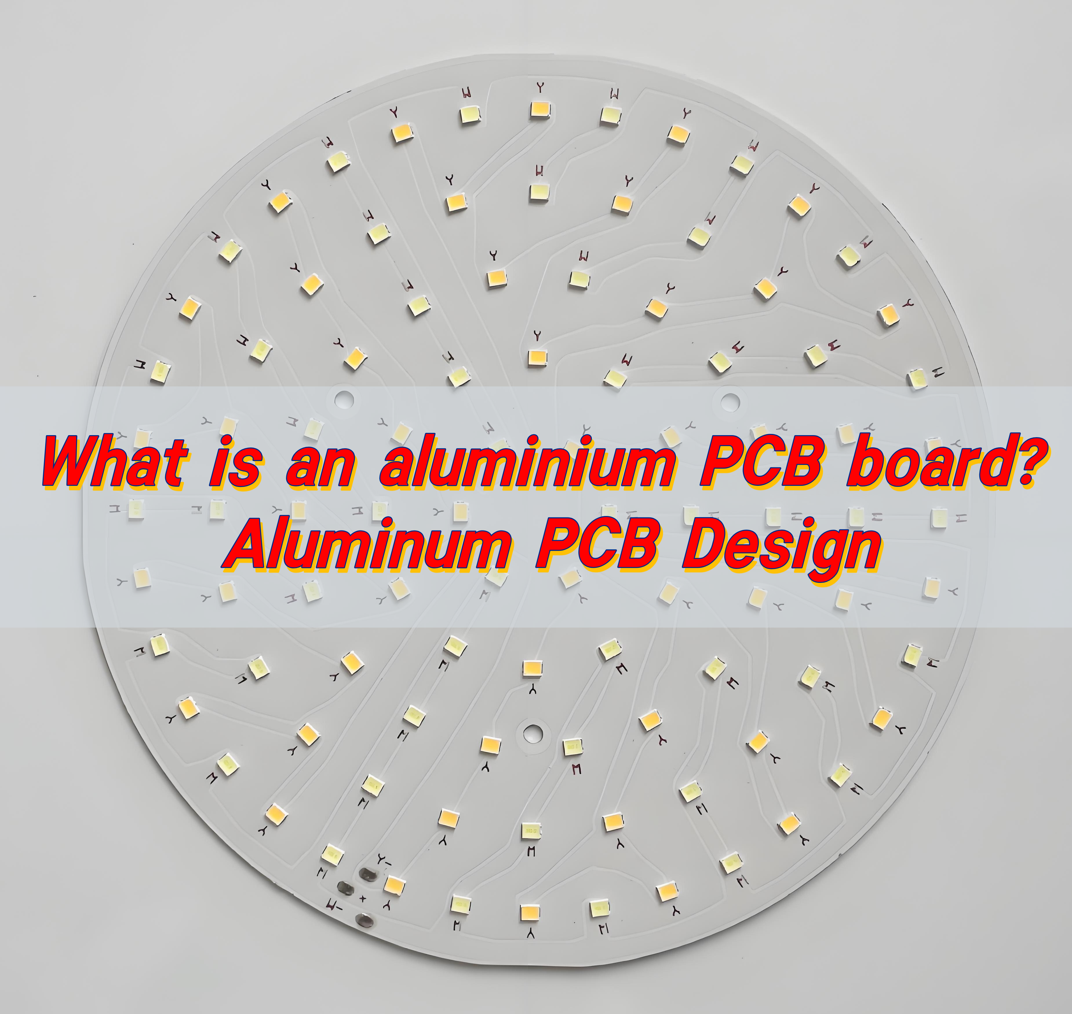
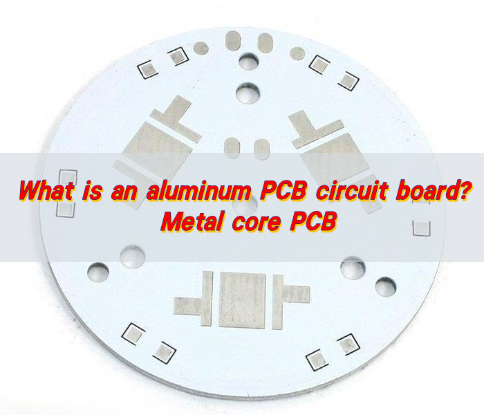
Aluminium PCB boards are metal-based printed circuit boards with an aluminum alloy substrate. Their thermal conductivity is dozens of times higher than that of traditional FR-4, allowing them to quickly dissipate heat from chips and prevent failures caused by hot spots. Combined with highly reflective white oil and a thin insulating layer, they serve as both a circuit and a heat sink, making them widely used in LED lamps, power modules, and automotive electronics.
How to make aluminium PCB board?
Making an aluminium PCB board involves precision and the right materials. It starts with choosing a quality aluminium substrate. It’s then coated with an insulating dielectric layer, which isolates the conductive copper from the metal.
Next comes copper lamination. A thin sheet of copper is pressed onto the dielectric surface. This copper layer will form the circuit paths. Once laminated, the board is cleaned and coated with a photoresist. Ultraviolet (UV) light exposure follows, using a circuit design mask to harden certain parts of the photoresist.
Unexposed areas are washed away, revealing the pattern. The exposed copper is then etched off, leaving behind the circuit layout. After this, any remaining photoresist is stripped. Now the board is cleaned and goes through a surface finish process, such as HASL or ENIG, depending on the end-use.
Finally, the board is cut into shape and tested for functionality. Every step is crucial for ensuring electrical performance and heat resistance.
How does the aluminium PCB manufacturing process work?
Material preparation: Choose an aluminium base, usually with a thickness of 0.8mm to 3.0mm. Apply a thermal insulation layer and copper foil.
Lamination: Bond the dielectric and copper layers tightly to the aluminium. Heat and pressure ensure this bond holds firm.
Imaging: Apply a photoresist film and expose the board under UV light. The light hardens the areas forming the copper traces.
Etching: Remove unwanted copper using chemical solutions. Only the protected areas from imaging remain.
Drilling and Plating: Drill precise holes for component leads or vias. Plate these holes if needed.
Solder Mask and Surface Finish: Apply a protective solder mask to non-conductive areas. Add a surface finish to enhance solderability and corrosion resistance.
Testing: Perform electrical tests to check for shorts, open circuits, and reliability.
Profiling: Cut the board to the desired size and shape.
These steps are controlled tightly. That’s why working with an experienced aluminium PCB manufacturer is critical.
How to design an efficient aluminum PCB?
Designing an effective aluminium PCB starts with understanding its strengths. Heat management is the top reason to use aluminium. Start by placing high-power components closer to the metal core. This reduces thermal buildup.
Keep trace lengths short and direct. This minimizes resistance and power loss. Use wider traces for higher current paths. Layer stack-up also matters. A single-layer design is often enough for LED and power circuits. For more complex boards, consider a multilayer design.
Thermal vias can help in spreading heat, especially in multilayer boards. Select the right thickness for your dielectric layer to ensure proper insulation and heat flow.
When choosing the surface finish, think about the end application. ENIG works well for fine-pitch components. HASL is good for general use.
Excellent aluminum PCB design balances electrical, mechanical, and thermal performance. Choose BEST Technology, you will get the best aluminum PCB design
What are the layers of aluminum PCB?
Aluminium PCB boards generally have three layers:
Aluminium Base Layer: This is the mechanical support and heat conductor. It’s usually made of alloy 5052 or 6061 for strength and heat resistance.
Dielectric Layer: Placed between the base and copper foil. This insulation layer resists heat and electrically isolates the copper traces. Thickness varies from 50µm to 200µm.
Copper Layer: This is the conductive layer where the circuit forms. Thickness can range from 1oz to 3oz depending on current requirements.
Some designs include additional layers:
Solder Mask: Applied over the copper to prevent oxidation and short circuits.
Silkscreen: For labeling component placements and orientation.
These layers combine to offer durability, high thermal conductivity, and efficient current flow in one compact board.
What is the highest temperature aluminum PCB can withstand?
Aluminium PCBs are built to handle high heat. Their metal base and insulating layer offer much better thermal management than standard FR4 boards. Depending on the material used, aluminium PCBs can endure temperatures between 120°C to 150°C continuously.
For short durations or pulse heating, they can handle spikes up to 250°C. Some high-grade aluminium PCBs, with advanced dielectric materials, may go even higher.
This heat resistance makes them ideal for LED lighting, automotive controls, and power converters. Proper design and material selection can ensure your board works reliably in high-heat environments.
Can aluminum PCB support high frequency signals?
Yes, aluminium PCB boards can support high frequency signals. But it depends on the quality of the dielectric layer. A low-loss dielectric material ensures signal stability.
In high-frequency applications, such as communication devices and radar systems, signal integrity is crucial. Aluminium PCBs with high-performance dielectric can deliver clear, uninterrupted signals.
Design also plays a role. Keep signal paths short and separate analog from digital traces. Ground planes and impedance control improve performance even more.
Though aluminium PCBs aren’t the first choice for all RF applications, they work well in many mid-frequency designs.
How strong is FR4 compared to aluminum?
FR4 is the standard fiberglass material used in many PCBs. It’s lightweight, low-cost, and electrically reliable. But when it comes to strength and heat resistance, aluminium is superior.
Aluminium offers better mechanical support. It doesn’t warp under heat like FR4. It also dissipates heat much faster, which is vital in LED or power circuits.
FR4 works well for multi-layer signal processing boards. But for durability, thermal control, and stability, aluminium PCBs outperform FR4 in harsh conditions.
So, if your project demands strength and heat resistance, aluminium PCB is the better choice.
How does aluminum PCB compare to rigid flex and HDI PCB?
Aluminium PCBs, rigid flex PCBs, and HDI PCBs each serve different needs.
Aluminium PCB: Best for heat-intensive applications. Offers strong thermal management and mechanical strength.
Rigid Flex PCB: Combines flexibility and rigidity. Perfect for compact devices with moving parts like cameras or foldable screens.
HDI PCB: Designed for high-density circuits with microvias. Used in smartphones, tablets, and miniaturized electronics.
If your design demands heat dissipation and durability, aluminium wins. If space-saving and flexibility are key, go with rigid flex. For high-speed, high-density circuits, HDI is the way to go.
Conclusion:
Aluminium PCB boards are powerful and reliable. In many cases, they outperform traditional solutions in terms of heat dissipation and mechanical strength. Whether you’re working on LED lighting, power electronics, or high-frequency devices, Aluminium PCB boards provide a solid foundation.
Choose a professional partner to get the best results. At EBest Circuit (Best Technology), we specialize in high-quality aluminium PCB boards with custom design support and fast delivery.
If you are developing lighting products, displays, or electronic devices that use LEDs, then LED PCB assembly is a crucial step in turning your idea into a working product. Among many requirements, 94v0 LED PCB assembly is one of the most requested because of its fire-resistant properties. Whether used in indoor lighting, automotive systems, or industrial equipment, the quality of the assembly process plays a key role in how well an LED product performs and how long it lasts.
At EBest Circuit (Best Technology), we provide full turnkey LED PCB assembly services tailored to meet global quality standards. Our facility in China is certified to ISO9001, IATF16949, ISO13485, and AS9100D, so we can serve various industries. We support both prototypes and high-volume production and no minimum quantity requirements.
What is a LED PCB?
A LED PCB is a specialized circuit board designed to support and power LEDs efficiently. Unlike traditional PCBs, LED PCBs often require better thermal management because LEDs generate significant heat during operation. To solve this, metal core PCBs, especially aluminum-based PCBs, are commonly used for LED applications. These boards offer excellent heat dissipation and mechanical stability.
Key Features of LED PCBs:
Metal Core Base (Often Aluminum and copper): Helps manage heat generated by LEDs.
Copper Traces: Conduct electricity efficiently.
Solder Mask and Surface Finish: Protect the board and enhance durability.
Customized Shapes and Sizes: Designed based on the final product’s form.
LED PCBs are widely used in lighting fixtures, automotive headlights, backlit displays, signage, and industrial illumination systems. Their main advantage is efficient heat dissipation, which prolongs the LED’s lifespan and ensures consistent brightness.
LED PCB Without Components
LED PCB vs LED PCB Assembly
Understanding the difference between a LED PCB and LED PCB assembly helps clarify the scope of your project needs.
A LED PCB refers to the bare printed circuit board that includes copper tracks and pads but no components mounted on it.
LED PCB assembly is the full process of mounting LEDs and other electronic parts on the PCB to make it functional.
If you only order the PCB, it won’t work until it goes through the assembly process. At EBest Circuit (Best Technology), we handle both PCB fabrication and LED PCB assembly, saving you time and reducing the risk of issues between design and production.
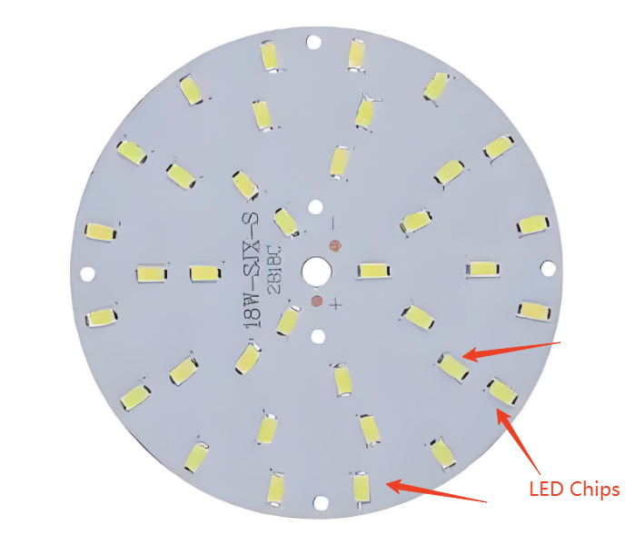
LED PCB Assembly with LED Chips
Detailed LED PCB Assembly Process
The LED PCB assembly process is a multi-stage procedure that demands strict quality control at every phase. Below is a detailed breakdown of how EBest Circuit (Best Technology) handles LED PCB assembly from start to finish. We deeply know the importance of quality, so each step are well-controlled to ensure the final product performs reliably.
1. File Review and BOM Verification
Before anything begins, our engineers carefully review your Gerber files, Bill of Materials (BOM), assembly drawings and perform DFM check to ensure compatibility and avoid errors. If there are any problems, our guys will send approvements to you for approval and continue until get your confirmation!
2. Component Procurement and Inspection
The process begins with sourcing high-quality LEDs and supporting components like resistors, capacitors, and connectors. We work only with trusted suppliers like mouser, digikey, find chips to ensure that all components meet performance and safety standards. Upon arrival, all components undergo incoming quality control (IQC), including visual inspection, functional testing, and packaging verification. In EBest Circuit (Best Technology), we support partial components sourcing, that means you can provide components or provide partial components to us.
3. Solder Paste Printing
Solder paste is applied to the solder pads on the bare PCB using a stencil printer. This step is critical because the quantity and placement of solder paste directly influence the quality of the solder joints. We use automated stencil printing machines to apply the paste consistently across all boards, ensuring optimal solder volume and alignment. After printing solder paste, we will perform SPI inspection to make sure the evenly paste spreading.
4. SMT Pick and Place
Once the solder paste is printed, the board moves to the pick and place stage, where automated SMT machines precisely place each component on the board. LEDs must be correctly oriented and positioned to maintain consistent brightness and color uniformity. Our pick and place machines handle small SMD LEDs (01005 sizes) as well as larger power LEDs with high accuracy.
5. Reflow Soldering
The boards with placed components are passed through a reflow oven. The oven heats the board in a controlled temperature profile that melts the solder paste and solidifies the electrical connections. Each LED PCB requires a customized reflow profile to avoid damaging sensitive LEDs and ensure strong, void-free solder joints.
6. AOI Inspection (Automated Optical Inspection)
After reflow soldering, we perform AOI inspection using high-resolution cameras that scan the entire board for defects such as misaligned components, solder bridges, insufficient solder, or missing parts. AOI helps detect errors early, reducing rework and ensuring product reliability.
7. Functional Testing
Functional testing is essential for LED PCB assembly. We power up each board to verify that all LEDs light up properly, and test for brightness, color temperature, voltage, and current draw. Any boards that fail the test are isolated and analyzed to determine the cause.
Common LED PCB Assembly Defects and Analysis
Even with advanced machines and experienced engineers, LED PCB assembly can face challenges. Understanding common defects helps prevent quality issues and reduce product failure in the field. Below are typical types of defects, their causes, and how we address them.
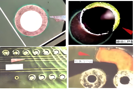
Virtual Soldering (Cold Solder Joint)
This occurs when the solder doesn’t properly bond to the component lead or pad. It often happens due to oxidized leads, contaminated surfaces, or incomplete solder melting. These joints can lead to intermittent connections, flickering LEDs, or total circuit failure.
Pad Lifting
Prolonged heating or excessive temperature during rework may cause the copper pad to detach from the PCB substrate. This defect is common when the PCB lacks proper thermal resistance or heat treatment was not controlled during manufacturing.
Solder Bridging (Short Circuit)
When too much solder paste is applied or components are placed too closely, it can create a bridge of solder between adjacent pins or pads. This causes unexpected electrical connections, leading to short circuits or component failure.
PCB Warping or Cracks
Improper material selection, uneven thermal expansion, or poor lamination techniques can cause the board to warp or crack. This leads to misalignment of components and can even cause open circuits due to mechanical stress.
Moisture Absorption
If the PCB is not properly baked before assembly, it may retain moisture. During reflow soldering, trapped moisture vaporizes, forming bubbles or delamination, which can damage internal layers or cause short circuits.
Poor Heat Dissipation
LEDs generate heat, and insufficient thermal design—such as no heat sink, poor copper thickness, or inadequate via design—can lead to LED overheating, early lumen degradation, or even component burn-out. This is critical in high-power LED assemblies.
Inadequate Spacing Between Traces or Pads
If the design leaves insufficient spacing between LED pins or traces, it raises the risk of short circuits during soldering, especially with high current LED applications.
Misalignment Between PCB Layers
In multi-layer LED PCBs, improper consideration of thermal expansion coefficients or misalignment during layer stacking may cause warping during soldering, affecting overall reliability.
No Pre-Baking
Flexible LED strips or moisture-sensitive components should be pre-baked before soldering. Skipping this step may result in component cracking, color variation, or reduced LED lifespan.
How We Prevent These Defects?
At EBest Circuit (Best Technology), we take proactive measures to reduce these risks:
Design Optimization: We assist clients with DFM (Design for Manufacturability) to improve spacing, heat dissipation, and alignment.
Controlled Processes: We monitor solder paste thickness, reflow oven temperature, and component placement accuracy using real-time SPC systems.
Material Handling: All PCBs are pre-baked to remove moisture, and we use appropriate solder pastes based on the design and LED type.
Inspection and Testing: AOI, X-ray, and functional testing help us catch any defect early and ensure that each LED assembly works correctly
How We Ensure the Highest Quality During LED PCB Assembly?
At EBest Circuit (Best Technology), delivering high-quality LED PCB assemblies is our top priority. Here’s how we maintain consistent quality:
Advanced Equipment
We invest in automated and high-precision machines for every step of assembly. Our AOI systems, reflow ovens, and pick and place machines are regularly maintained and calibrated to ensure accuracy.
Skilled Technicians and IPC Standards
All assembly work is carried out by trained personnel who follow IPC-A-610 standards for electronic assemblies. Our team’s experience helps us tackle complex assemblies with confidence.
MES System and Traceability
We use a Manufacturing Execution System (MES) to monitor production in real-time. Each board has a unique traceability code, allowing us to track its production history, components used, and test results.
Quality Audits and Final Inspection
Before shipping, every batch undergoes final quality control (FQC), including random sampling and full functional testing. This ensures that our customers receive only fully functional and reliable LED PCBs.
LED PCB Assembly Machines We Use
Reliable LED PCB assembly depends on the quality of equipment used. At EBest Circuit (Best Technology), we invest in modern assembly machines that allow for fast, accurate, and repeatable results. Our equipment includes but not only:
Yamaha & Juki Pick-and-Place Machines
Solder Paste Printers (Fully Automated)
3D SPI Inspector
Nitrogen Reflow Oven
Dual Online AOI Machine
X-ray Inspection
FAI tester
PT-500M-2ABN loader
Dry Ice Cleaner
Selective Wave Soldering
Multiply Aging Testing
Our 94v0 LED PCB Assembly Daily Capabilities
94v0 LED PCBs are manufactured using flame-retardant materials that meet UL94V-0 standards. This rating indicates that the material self-extinguishes quickly after being exposed to a flame, which is crucial for safety. Here’s what we offer daily:
Daily Output: Up to 10,000 LED PCBs depending on complexity.
Board Types: Rigid, flexible, aluminum-core, and copper-core boards.
LED Options: Standard SMD LEDs, COB (chip on board), and high-power LEDs.
Applications: LED lighting fixtures, automotive lights, medical devices, signage, and industrial systems.
Customization: We support custom shapes, multiple layers, and specialized surface finishes.
Minimum Order Quantity: No strict MOQ; we accept small-batch and large orders.
Prototyping Speed: 3–5 working days for prototypes.
China LED PCB Assembly Manufacturer – EBest Circuit (Best Technology)
When it comes to LED PCB assembly in China, having a dependable partner can make a big difference in your product’s quality, lead time, and overall success. At EBest Circuit (Best Technology), we specialize in delivering high-quality LED PCB assembly services tailored to your needs—whether you’re developing lighting systems, automotive LEDs, or consumer electronics.
Here’s why companies worldwide choose us:
One-stop Service: From PCB fabrication to full assembly, testing, and packaging, we handle every step in-house.
Fast Turnaround: Whether you need prototypes or large-scale production, we offer quick turnaround times, clear communication, and reliable delivery.
Competitive & Transparent Pricing: Direct factory pricing with no hidden costs.
Professional Support at Every Stage: Our experienced engineers help with design review, material selection, and process optimization, so your project runs smoothly from start to finish.
Flexible Order Quantities: We handle both prototyping and mass production with equal attention to detail.
Smart Manufacturing: With our MES system, we track every board throughout production, giving you full traceability and confidence in product quality.
If you’re looking for a China-based LED PCB assembly manufacturer that delivers quality, speed, and peace of mind, EBest Circuit (Best Technology) is here to support you. Contact us today for a quote or to discuss your next project—we’re ready to help.
FAQs
1. What does 94v0 mean in LED PCB assembly?
It’s a UL rating for flame-retardant PCBs, meaning the material self-extinguishes after ignition, ensuring safer products.
2. What is the difference between aluminum and FR4 for LED PCBs?
Aluminum provides better heat dissipation and is ideal for high-power LEDs. FR4 is suitable for low-power or budget-friendly applications.
3. What types of LEDs can you assemble?
We assemble SMD LEDs, COB LEDs, high-power LEDs, and custom LED arrays for various applications.
4. How do you ensure the LEDs won’t overheat?
We use metal core PCBs, apply thermal pads, and follow optimized reflow profiles to manage heat effectively.
5. Do you offer testing for assembled LED PCBs?
Yes, we offer functional testing, burn-in testing, and optional aging tests for long-term reliability.
6. What’s the typical lead time for LED PCB assembly?
Prototypes: 3–5 working days; volume orders: 7–15 days depending on complexity.
7. Do you support custom designs?
Yes, we support custom LED PCB designs, including unique shapes, sizes, and special surface finishes.
8. How can I get a quote for LED PCB assembly?
You can send us your Gerber files, BOM, and specifications. Our team will provide a clear, competitive quote within 24 hours.
An aluminium PCB circuit board, or metal core PCB, is a type of circuit board built on an aluminum base for better heat dissipation. Unlike standard FR-4 boards, it handles high temperatures and heavy loads with ease.
It’s commonly used in LED lighting, automotive systems, and power electronics where performance and durability matter.
How to make aluminum PCB?
Making an aluminium PCB circuit board involves several precise steps. Each layer plays a role in the board’s thermal, electrical, and structural performance.
Aluminum Base Layer: This is the bottom layer and acts as the backbone. It’s made from high-quality aluminum alloy that’s strong, lightweight, and thermally conductive.
Dielectric Layer: This insulating layer sits between the aluminum and copper. It transfers heat efficiently while keeping electrical signals safe.
Copper Layer: This is where the actual circuitry is formed. Copper is etched to create the pathways that electrical signals follow.
Solder Mask and Silkscreen: The solder mask protects the copper from oxidation and short circuits. The silkscreen marks component placements and part numbers.
Drilling & Surface Finishing: Holes are drilled for component leads. Surface finishes like ENIG or HASL are applied to improve solderability.
Every step demands precision. At EBest Circuit (Best Technology), we fine-tune this process to create aluminum PCBs that meet strict quality standards.
What is the structure of aluminum PCB?
The structure of an aluminum circuit board is simple but effective:
Metal Core (Aluminum Layer): Offers mechanical strength and heat sinking.
Thermal Dielectric Layer: Transfers heat away from the copper layer.
Copper Circuit Layer: Routes the signals and power across the board.
Depending on the design, it can be:
Single-layer: Common for LED applications.
Double-layer: For more complex circuits.
Multilayer: Combines performance and compact size.
Rigid-flex: For advanced or tight-space applications.
Each type supports different applications but shares the same core benefit—effective thermal management.
How thick is aluminum PCB?
The thickness of an aluminium PCB circuit board varies based on the application:
Aluminum Base Layer: Typically ranges from 0.8mm to 3.2mm.
Copper Layer: 1oz to 3oz (35μm to 105μm).
Dielectric Layer: Between 100μm and 200μm.
Thicker boards offer better heat dissipation and mechanical strength, while thinner boards save space and cost. The right choice depends on power levels, component density, and enclosure design.
What is the maximum temperature for aluminum PCB?
Aluminum PCBs are designed to handle heat with ease. In most cases, they can operate continuously between 130°C and 150°C. During brief soldering processes, they can withstand up to 250°C.
This makes them perfect for high-temperature environments, especially in LED lighting and power electronics. But, performance depends on:
Copper weight
Quality of the dielectric layer
Circuit design and cooling system
At EBest Circuit (Best Technology), we choose high-grade materials to ensure long-lasting temperature stability.
What are the pros and cons of aluminum PCB?
Let’s start with the advantages:
Superior Heat Dissipation: Heat moves quickly away from sensitive parts. This boosts performance and extends product life.
Lightweight Yet Durable: Aluminum is stronger than FR-4 and lighter than ceramic boards.
Eco-Friendly: Aluminum is recyclable, reducing environmental impact.
Cost-Effective for Power Applications: Reduces need for extra heat sinks and thermal pads.
And now the few limitations:
Not as flexible as polymer-based PCBs
Slightly higher initial cost than FR-4 (but lower maintenance and longer lifespan)
In real-world use, the advantages far outweigh the disadvantages, especially since it is designed and manufactured by BEST Technology.
What is the difference between aluminum and FR-4 PCB?
Let’s compare the two:
Feature
Aluminum PCB
FR-4 PCB
Thermal Conductivity
High, handles heat well
Low, needs heat sinks
Material
Metal core (Aluminum)
Fiberglass epoxy (FR-4)
Durability
Tough, resists shock
Less impact-resistant
Cost (initial)
Slightly higher
Lower
Cooling Accessories
Often not needed
Frequently needed
Weight
Moderate
Lightweight
If your project involves high power or heat-sensitive components, aluminum wins hands down.
When to use aluminum PCB?
Aluminum PCBs aren’t for everything, but when heat is involved, they’re unbeatable.
Use them in:
LED lighting (especially high-brightness)
Power supply modules
Automotive electronics
Electric vehicle components
Communication base stations
Audio amplifiers
They’re also great when you want to reduce size and weight without sacrificing strength.
What are aluminum PCBs used for?
These boards are everywhere, though often hidden inside devices:
1. LED Applications: LEDs produce heat, and aluminum PCBs are ideal for pulling that heat away. This prevents light degradation and extends lifespan.
2. Automotive Systems: Cars generate vibration, heat, and require stability. Aluminum PCBs resist shock and stay cool—perfect for control modules and lighting.
3. Power Electronics: Used in DC/AC converters, battery management systems, and solar inverters.
4. Industrial Controls: Drive controllers, motor regulators, and sensors need tough, reliable PCBs. Aluminum handles the stress and heat like a pro.
5. Medical Equipment: From diagnostic machines to surgical lighting, these boards maintain performance and safety in critical conditions.
6. Telecommunication Systems: They provide reliability in routers, amplifiers, antennas, and base stations.
Aluminum PCBs support modern devices across industries, from smart homes to renewable energy systems.
Conclusion:
Aluminium PCB circuit boards bring the perfect mix of strength, efficiency, and thermal control. They handle harsh environments and extend the lifespan of electronics. Their use in electronic products is increasing due to their superior thermal management, improved durability and long-term cost-effectiveness.
At EBest Circuit (Best Technology), we specialize in high-performance aluminum PCB design and manufacturing. Our boards are built to meet international standards and customized to your needs.
Want to upgrade your products with dependable aluminum PCBs? Contact us today at: sales@bestpcbs.com
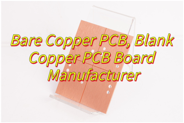
What is bare copper PCB? Let’s explore its benefits, applications, design guide, design spec, manufacturing process, manufacturer selection methods.
Are you worried about these problems?
Is your device overheating and throttling? — Do traditional FR-4 boards always force you to prioritize cooling under high load?
Is heat generation high in a small space? — In the pursuit of thinness and lightness, are performance or reliability sacrificed due to insufficient heat dissipation?
Is cooling cost difficult to control? — Does adding heat sinks and fans increase the BOM cost with limited effectiveness?
EBest Circuit (Best Technology) can provide solutions
Metal-Based Thermal Conductivity: Aluminum/copper substrates offer 5-10 times higher thermal conductivity, enabling rapid heat dissipation and stable operation in high-temperature environments.
Compact Design: Integrated metal-based molding eliminates the need for additional heat dissipation components, improving space utilization by 30%.
Total Cost Optimization: Reduces procurement and assembly costs for cooling modules, reducing overall lifecycle costs by 20%.
A Bare Copper PCB is an uncoated circuit board where the raw copper layer remains fully exposed. Stripped of traditional surface finishes like gold or tin plating, this design maximizes copper’s inherent properties, exceptional conductivity (5.9×10⁷ S/m) and thermal dissipation (400W/m·K). Ideal for high-frequency applications like 5G and power electronics, it offers cost savings (15-20% reduction) while maintaining signal integrity by eliminating plating-induced signal loss.
What Are Advantages of Blank Copper PCB?
Cost Efficiency – No additional surface finish (e.g., ENIG, HASL) reduces manufacturing costs by 15–30%.
Superior Conductivity – Pure copper provides low resistance, ideal for high-speed signals and low-loss power transmission.
Confirm support for multi-layer boards (e.g., 12–40 layers) and thick copper (≥2oz/70μm). Check minimum trace width/spacing (e.g., 3mil/0.0762mm) and via diameter (≥0.2mm).
Certification & Compliance
Prioritize manufacturers with ISO 9001 (quality), UL (safety), IATF 16949 (automotive), and RoHS (environmental) certifications. Ensure compliance with IPC-6012 (rigid PCB performance) and MIL-P-13949G (military/aerospace) if applicable.
Production Capacity & Delivery
Prototyping Speed: Look for 24-hour prototyping or faster for urgent projects.
Scalability: Ensure capacity for mass production (e.g., multiple automated production lines).
Quality Control
Testing: Require electrical testing (flying probe/fixture) and AOI inspection for defect detection.
Material Control: Verify copper thickness tolerance (±10%) and substrate quality (FR4/polyimide).
Industry Experience
Choose manufacturers with proven expertise in your sector (e.g., automotive, medical, or high-speed designs). Review case studies or client testimonials for validation.
Cost & Supply Chain
Compare pricing models for small/medium batches. Opt for manufacturers with scalable production to reduce per-unit costs. Consider geographic proximity to minimize logistics expenses.
Communication & Support
Assess responsiveness to technical queries and post-sales service. Ensure clear warranty terms and defect resolution processes.
Looking for copper metal core PCB thermal solution? Let’s explore spec, benefits, application, design guide and thermal solution, manufacturing process for copper metal core PCB.
Are you worried about these problems?
Is your LED product experiencing luminous efficacy degradation due to insufficient heat dissipation?
How can you avoid reliability risks when high-power devices experience uncontrolled temperature rise?
Struggling to balance cost and performance? How can you choose a lightweight solution?
EBest Circuit (Best Technology) can provide solutions
Precise Thermal Matching Service: Through thermal simulation modeling, we customize the copper layer thickness (available in 0.1-3.0mm), ensuring a 40% reduction in LED module junction temperature and a 50% reduction in lumen degradation.
High-Current Wiring Technology: Utilizing an immersion gold (Immersion Gold) + OSP process, it supports a continuous current of 5A/mm², eliminating overheating issues in power modules and increasing yield to 99.2%.
Lightweight Structural Design: Copper foil micro-etching technology achieves 50μm line/space widths. A multi-layer stacking solution reduces drone battery pack size by 20% and extends flight time by 15%.
A Copper Metal Core PCB (Printed Circuit Board) is a type of circuit board that uses copper as the base material instead of the traditional fiberglass (FR4). This metal core is typically located beneath the circuit layer and serves as a thermal conductor to dissipate heat generated by electronic components during operation. Copper metal core PCB has superior thermal conductivity, making it highly effective for managing heat in power electronics, LED lighting, automotive systems, and industrial control equipment.
Copper Metal Core PCB Specification
Parameter
Specification
Base Material
Copper (typically C1100 or similar high-purity copper)
Copper Core Thickness
0.5 mm, 1.0 mm, 1.5 mm, 2.0 mm, up to 5.0 mm (custom thickness available)
Up to 600 mm × 1200 mm (larger sizes possible upon request)
Drilling Options
Mechanical drilling, laser drilling for micro vias
Layer Count
Single-sided, double-sided, multilayer (up to 4 layers typical)
Impedance Control
Available for RF/high-frequency applications
Certification Standards
ISO9001, UL, RoHS, IPC Class 2/3 compliant
Benefits of Copper Substrate PCB
Exceptional Heat Dissipation: Copper’s high thermal conductivity (2x aluminum) rapidly transfers heat away from components, preventing overheating in LEDs, power modules, or automotive systems.
Longer Device Lifespan: Reduces thermal stress and component failure, extending reliability for high-current applications like EV chargers or industrial equipment.
Compact Design Flexibility: Thick copper layers enable dense circuits and smaller boards, saving space in 5G devices, RF systems, or medical electronics.
Cost-Effective Performance: Minimizes need for external cooling parts (fans/heatsinks), lowering long-term maintenance and material costs.
Versatile Application Fit: Ideal for high-power (solar inverters), precision (aerospace), and EMI-sensitive (radar) designs, ensuring stable operation in extreme environments.
Applications of Copper Metal Core PCBs
High-Power LED Lighting: Efficiently dissipates heat from dense LED arrays, preventing color shift and extending lifespan for automotive, industrial, and architectural lighting.
Automotive Electronics: Manages heat in power modules (e.g., engine control units, battery management systems) under extreme temperatures, enhancing reliability for EVs and hybrid vehicles.
5G & RF Devices: Supports high-frequency circuits and millimeter-wave components by minimizing thermal noise, critical for 5G base stations and radar systems.
Industrial Power Systems: Withstands high currents and thermal stress in motor drives, inverters, and solar power converters, reducing downtime and maintenance costs.
Aerospace & Defense: Provides lightweight, durable thermal management for avionics, satellite components, and ruggedized communication gear in harsh environments.
Low-temperature: Use high-Tg substrate (Tg>170°C); increase via density.
Copper Metal Core PCB Thermal Solution
1. Advanced Thermal Materials
Graphene-Enhanced Copper: Utilize copper-graphene composites (thermal conductivity up to 440W/mK) for core heating zones. Apply 10μm graphene films on copper layers to boost lateral thermal diffusion by 40%.
Staged Copper Thickness: Use 4oz copper for high-power areas (e.g., IGBTs), transitioning to 2oz in peripheral zones via teardrop-shaped (≤45°) connections.
2. Via Array Optimization
Thermal Vias: Deploy 0.3mm diameter vias in hotspots (density ≥4 vias/cm²), reducing thermal resistance by 90% compared to non-via designs.
Dynamic Spacing: Use hexagonal via patterns for heat flux >50W/cm²; rectangular arrays for <30W/cm². Maintain via spacing ≥2×via diameter +0.1mm.
Copper-Via Synergy: Thicken via walls to ≥30μm when outer-layer copper exceeds 35μm. Reduce via spacing to 0.8mm for 35μm copper layers.
3. Heat Pipe Integration
Embedded Heat Pipes: Insert 1.5mm-diameter heat pipes beneath IGBTs, filled with phase-change material. Limits local temperature rise to ≤15°C (5× more efficient than vias alone).
Patent-Proven Designs: Fix heat pipes to aluminum substrates via high-temperature soldering, ensuring direct contact with chassis for efficient heat dissipation.
4. Thermal Path Engineering
Vertical-Horizontal Hybrid Cooling: Combine 0.3mm vias (vertical heat transfer) with 0.5mm linewidth hexagonal grids (horizontal spreading) in non-critical zones.
Ceramic Insertion: Embed AlN ceramic pads (thermal conductivity 320W/mK) under power modules, bonded with silver paste to achieve baseplate thermal resistance <0.15°C/W.
5. Simulation & Validation
Thermal Modeling: Use ANSYS Icepak with 3× denser mesh in via regions. Validate against real-world data (e.g., 48V DC/DC module via optimization reduced thermal resistance from 1.2°C/W to 0.78°C/W).
Infrared Testing: Confirm design efficacy via thermal imaging, ensuring peak junction temperatures stay below 125°C (with <10°C rise per 10% power increase).
6. Manufacturing Adjustments
Aspect Ratio Control: Maintain via diameter-to-board thickness ratio ≤10:1. Tolerance: ±0.05mm for vias ≤0.8mm.
Solder Mask Management: Expand solder mask 0.1mm beyond pads; remove mask entirely in thermal via arrays to enhance heat dissipation.
Star MCPCB is a reliable solution for LED lighting systems that require consistent thermal management and high brightness. When developing LED prototypes, using a well-designed MCPCB star board helps ensure steady performance and longer lifespan. However, finding a dependable supplier for small batches often challenges engineers and buyers alike. At EBest Circuit (Best Technology), we provide fast, quality service to help customers overcome this issue, improving both inquiry efficiency and product outcomes.
EBest Circuit (Best Technology) is a Chinese Star MCPCB Manufacturer, providing DFM analysis, prototype, fabrication, SMT assembly, and box build service. Rigorous quality control system, rich design and manufacturing experience, sophisticated equipment and technology, quick response, and short lead times really puts a competitive edge to us over the average metal core manufacturers. Our factory supports multiple materials and the customized sizes that meet a variety of LED application needs. Just connect with us at sales@bestpcbs.com for comprehensive solutions.
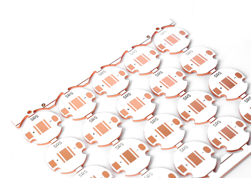
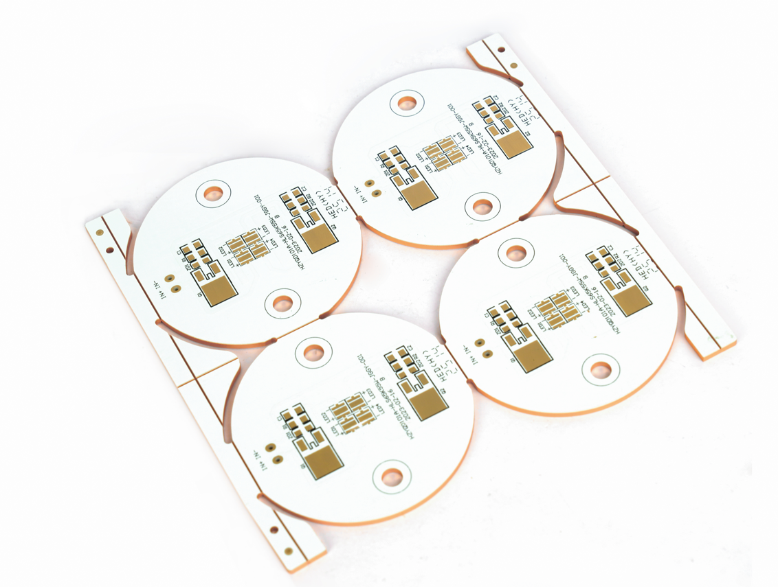
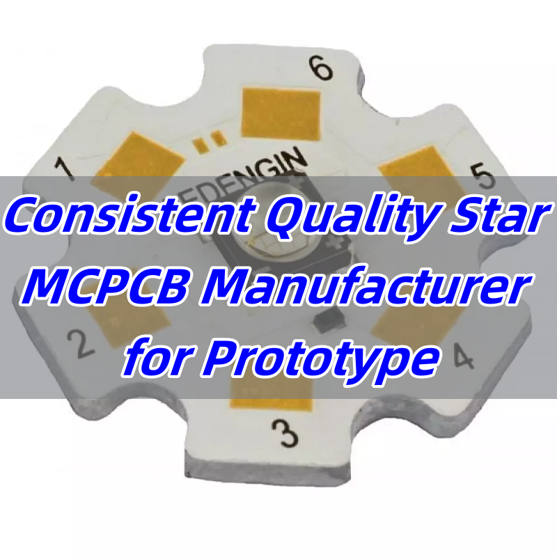
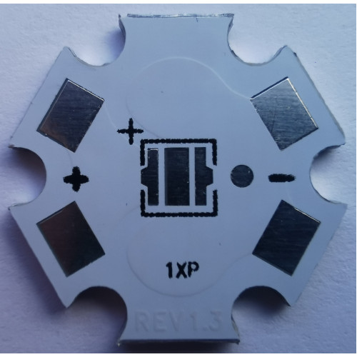
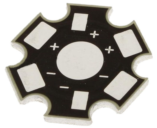
What is a Star MCPCB?
Star MCPCB refers to a metal core PCB shaped like a star or hexagon, typically used in LED lighting. It consists of a copper layer for circuitry, a dielectric for insulation, and a metal base (usually aluminum) for heat dissipation. These boards help LEDs maintain brightness while managing heat effectively. They are small, lightweight, and ideal for use in compact lighting assemblies.
What is the Material of Standard Star MCPCB?
Most standard star MCPCBs use aluminum as the base material because it is both cost-effective and efficient in conducting heat. The circuit layer uses copper, often 1oz or 2oz thickness. Between these layers is a thermally conductive dielectric, which enables fast heat transfer while ensuring insulation. These materials combine to form a durable, high-performance board for LED applications. At EBest Circuit (Best Technology), we use only RoHS-compliant materials, which are safe and environmentally friendly.
What are the Star MCPCB Dimensions?
Star MCPCB dimensions vary based on LED type and application. Standard sizes include 20mm, 16mm, and 12mm in diameter, with thickness typically around 1.0mm to 1.6mm. Custom shapes and sizes are also available. Our engineers support flexible design options to match specific customer needs. Importantly, tight tolerance is kept to maintain performance and ease of assembly.
How to Do the MCPCB Design?
MCPCB design begins with selecting the proper LED footprint. For star MCPCBs, this often includes layouts for 1W, 3W, or 5W LEDs. Designers need to focus on pad spacing, thermal paths, and hole placement. Clearances should match LED manufacturer guidelines. EBest Circuit (Best Technology) supports customers with DFM (Design for Manufacturing) checks, which help identify design risks before production. This reduces delays and avoids costly revisions.
What Are the Manufacturing Processes of the MCPCB LED Star?
Producing an MCPCB LED star involves several steps:
Copper Clad Laminate Cutting: Sheets are cut to size based on the required star shape.
Drilling: Holes for LED placement or mounting are drilled using precise tools.
Imaging: Circuit patterns are printed using photoresist methods.
Etching: Unwanted copper is removed to form the correct traces.
Dielectric Application: A thermal dielectric is layered for insulation.
Solder Mask and Surface Finish: These protect copper and improve solderability.
Routing and Final Shaping: Boards are cut into star shapes, and edges are cleaned.
Our advanced equipment ensures repeatable, accurate production even for small batches.
What is the Quality Inspection Process During LED Star MCPCB Manufacturing?
Quality is critical. At EBest Circuit (Best Technology), we perform the following checks during production:
Incoming Material Inspection: All raw materials are verified for conformity.
In-process Checks: Imaging, etching, and drilling are monitored for defects.
AOI (Automated Optical Inspection): Circuit accuracy is checked against design files.
Dielectric Strength Testing: Insulation is tested under voltage to prevent failures.
Final Inspection: Visual and mechanical checks ensure correct dimensions and finish.
Customers often worry about receiving inconsistent quality in prototypes. Our strict process and MES system (Manufacturing Execution System) help maintain traceability and consistency from start to finish.
What Are the Applications of the MCPCB Star Board?
MCPCB star boards are widely used in LED lighting, including:
They support both high and low-power LEDs. Due to the star shape, they are easy to mount onto heat sinks, which helps extend LED life. Our customers in Europe and the US often request customized designs for unique lighting projects, and our fast prototyping service helps them meet tight deadlines.
Where to Get MCPCB Star Board?
Choosing a dependable supplier for MCPCB star boards can greatly improve project outcomes. At EBest Circuit (Best Technology), we understand the value of both time and budget. That’s why we provide reliable support at every stage—from design to final delivery.
1. Full-Service Support from Start to Finish
We assist with design, material selection, and layout optimization.
Fast and accurate quotations help you plan your costs easily.
Rapid prototyping ensures you meet tight deadlines without stress.
2. Quick and Responsive Communication
We reply to all inquiries promptly.
Our engineering team offers practical solutions for your specific needs.
You will always know the status of your order.
3. Solving Common Customer Pain Points
Delay: We shorten lead times with efficient processes.
Poor Communication: We keep you informed at every step.
Inconsistent Quality: Strict quality checks ensure reliable boards every time.
4. Certified Quality You Can Trust
ISO 9001, ISO 13485, IATF 16949, and AS9100D certifications show our commitment to world-class manufacturing.
5. Consistent Quality for Every Order
Whether it’s a standard star MCPCB or a custom board, we deliver on time.
Quality is consistent, even for low-volume or prototype batches.
All in all, star MCPCB plays a key role in LED lighting. From efficient heat management to ease of installation, it supports reliable performance in various applications. However, sourcing quality boards quickly remains a challenge. EBest Circuit (Best Technology) helps customers overcome this by offering fast, reliable prototyping and production services. Our team’s experience, combined with strict quality control and responsive communication, helps customers improve project outcomes and reduce risks. Contact EBest Circuit (Best Technology) at sales@bestpcbs.com for better star MCPCB solutions and experience dependable support from design to delivery.