The color of a circuit board might seem like a simple design choice, but it holds significance in the electronics industry. Traditionally, green circuit boards have been the standard in most electronic devices due to their historical and functional advantages. However, blue circuit board is becoming increasingly popular across various sectors, from consumer electronics to custom devices.
Blue PCBs not only provide a pretty appearance but also serve specific functional purposes. Understanding the differences between blue and green PCBs can help you choose the best option for your project.
What Does a Blue Circuit Board Mean?
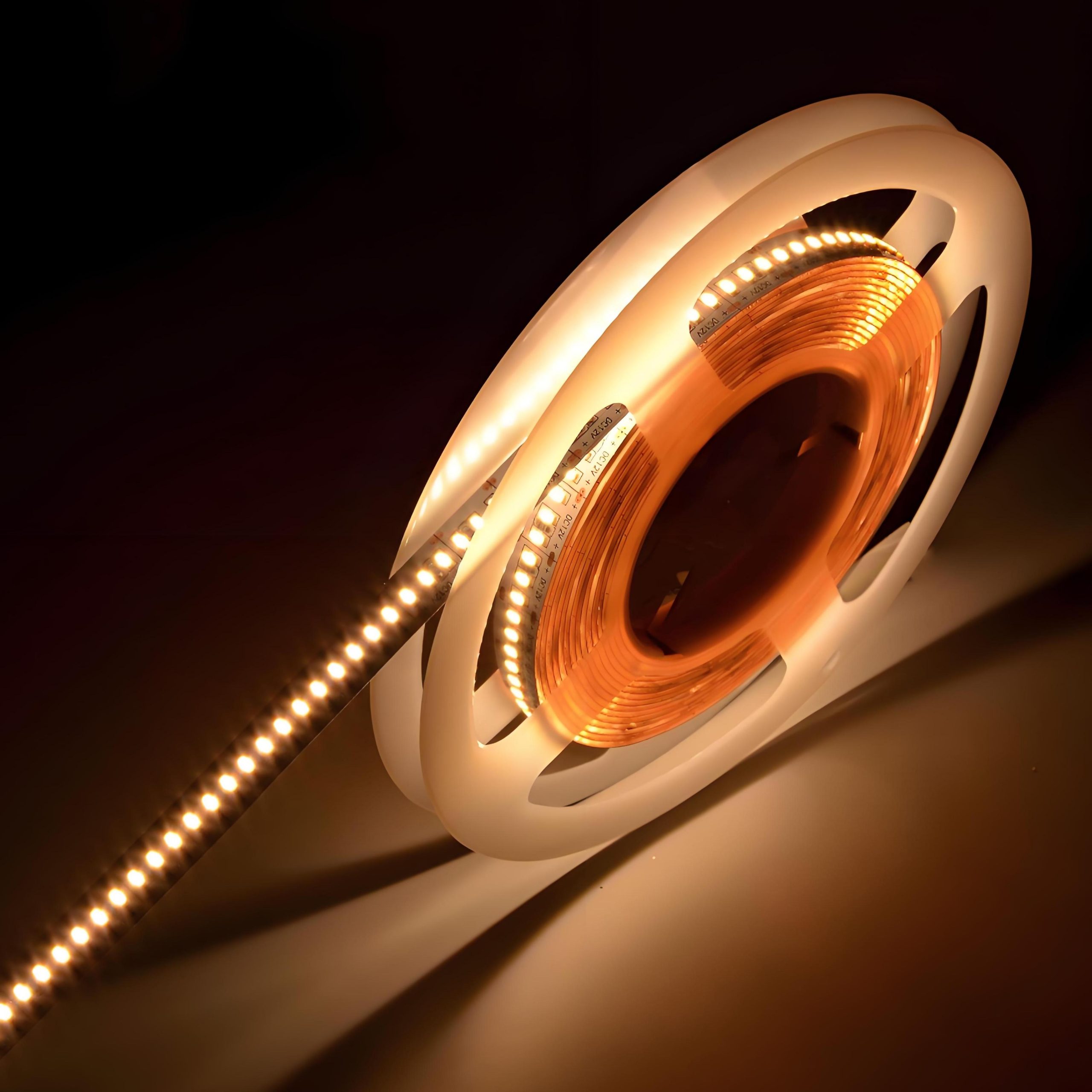
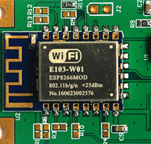
What does a blue circuit board mean? A blue circuit board, or blue PCB, refers to a printed circuit board with a solder mask of blue color. The solder mask is a protective coating applied over the copper traces on the PCB, preventing oxidation, short circuits, and solder bridges. While the color itself does not affect the board’s electrical properties, it influences other aspects such as visibility, inspection, and aesthetics.
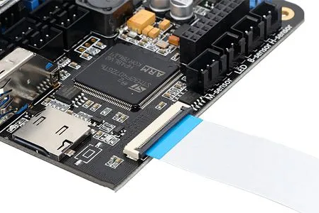
Blue PCBs are often associated with high-end electronics, prototypes, and custom designs. Their distinct color can make a product stand out, particularly in markets where branding and visual appeal are crucial.
Types of Blue PCB
Blue PCBs are available in various shades and finishes, each suited for specific applications and design preferences.
1. Dark Blue Circuit Board
Dark blue PCBs are commonly used in professional and high-end electronics. They have a deep color provides excellent contrast with white silkscreen text. So making the component labels and circuit paths easy to read.
2. Light Blue Circuit Board
Light blue PCBs are often used in consumer electronics where a bright, modern appearance is desired. The lighter shade has a clearly visibility during manual assembly and inspection, especially under low lighting conditions.
3. Matte Blue Circuit Board
This is a very advanced color. Matte blue PCBs feature a non-reflective finish that reduces glare and provides a more understated look. This finish is popular in devices where aesthetics and readability are important.
4. Glossy Blue Circuit Board
Glossy blue PCBs have a shiny, reflective surface that enhances their visual appeal. While they look attractive, they may reflect light, make its inspection slightly more challenging under bright lighting.
Why Are Some Circuit Boards Different Colors?
The color of a circuit board comes from the solder mask applied during the manufacturing process. While green is the most common color, other colors such as blue, black, red, and even white are available. The choice of color can be influenced by several factors:
1. Aesthetic Preferences
Different colors are used to align with a product’s design or brand identity. For example, a company that emphasizes innovation might choose blue PCBs or red PCBs to convey a modern and forward-thinking image.
2. Functional Requirements
Certain colors offer better visibility for manual assembly and inspection. For instance, blue and green provide excellent contrast with common silkscreen colors.
3. Product Differentiation
In a competitive market, using a non-standard PCB color like blue can help a product stand out and attract more attention from customers.
4. Historical Factors
Green PCBs became the industry standard due to early manufacturing processes and the availability of green solder mask materials. Over time, this color was adopted as the norm, but advancements in technology have made other colors like blue more accessible.
The Role of PCB Colors
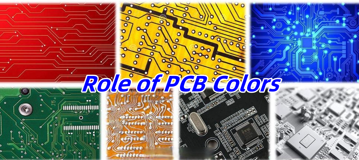
1. Green PCB
Green PCB is the most popular color. Therefore, many people have been mistakenly thinking that the PCB is green or most of it is green, green increases the clarity of the PCB, because the green PCB will have a sharp contrast with the white text, thus enhancing readability. In addition, the green PCB surface treatment reflects less light, helping to reduce glare.
2. White PCB
White PCB looks clean in a variety of environments, more and more popular. However, because the white PCB is easy to hide the line, white PCB is still not the first choice. But white PCBS look particularly contrasting in black screen printing.
3. Yellow PCB
In the past, yellow is one of more used colors in PCB solder mask, but now it is not so practical. Yellow PCBs can quickly meet different needs such as style, cleanliness and visibility. Yellow PCBs have one obvious disadvantage: poor contrast with wire and screen printing.
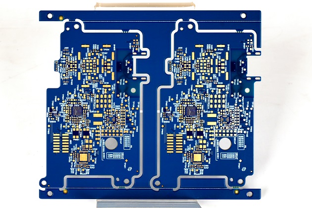
4. Blue PCB
Blue PCB is considered to be a thick plate for labels because it provides significant screen printing contrast. This PCB color is not as eye-catching as green PCB, black PCB, or white PCB, but blue PCB is the preferred PCB color because it provides an excellent aesthetic choice. Blue PCB installed on the LCD is better, because blue PCB does not produce sharp contrast edge and bright background color.
5. Red PCB
Because of the advantages of read PCB, many PCB manufacturers are still keen to adopt red. Red PCBs provide excellent visibility and clearly define contrast for trace, flat and white space. The screen print looks very beautiful against the red PCB.
6. Black PCB
Black PCB is as popular as white PCB. These two PCB colors produce low contrast and make it easy to mark important components. However, the main disadvantage of black and white PCBS is that specific details may focus light and have small shadows. This shadow makes tracking difficult. Therefore, it is not appropriate to use black PCB in various high temperature applications, because black PCB may discolor screen printing. Moreover, the black PCB board is a mixture of cobalt and carbon, and the electrical conductivity may be poor.
Blue vs. Green Circuit Board: Which Is Better?
We know, green is a standard solder mask color in the PCB, but blue also offers various advantages, so which one is better? Actually, choosing between a blue and green circuit board depends on the specific needs of your project. Both colors have their advantages and are suited for different applications.
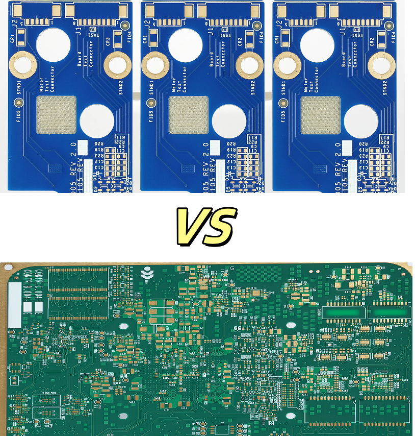
- Materials
The blue circuit board is also called FR-4 circuit board, and its substrate material is glass fiber reinforced epoxy resin. It is made by impregnating epoxy resin in glass fiber cloth and pressing it. This material can resist high temperature and humidity, so it is widely used in industrial fields.
The green circuit board, also known as the CCL circuit board, is made of fiberglass cloth and copper foil after high temperature and high pressure treatment, and the surface is covered with a welding mask. Its substrate material is the same as the blue circuit board, but the color is different. Green boards are relatively common because of their relatively low cost.
- Use
Blue circuit boards can resist high temperature and humidity, so they are widely used in industrial equipment and aerospace and other fields. Because of its stable performance and high security, the price is relatively high. However, green circuit board is suitable for small and medium-sized electronic products, such as household appliances, digital products, computer peripherals and so on.
- Cost
Blue circuit boards are relatively expensive because of their more stable performance. For green PCB, its cost is relatively low, but its safety and resistance to high temperature and humidity are worse than the blue circuit board.
4. Application Scenarios
It can be concluded from the above comparison that if the requirements for the circuit board are relatively high, such as used in industrial machines, it is recommended to choose the blue circuit board; If it is only the production of small and medium-sized electronic products, and the requirements for the circuit board are not so strict, you can choose a green circuit board.
Why Choose Blue Circuit Board?
Blue circuit boards are an excellent choice for projects that require a balance of aesthetics, functionality, and brand differentiation. Here’s why you might choose a blue PCB over a green one:
1. Enhanced Aesthetic Appeal
Blue PCBs offer a modern and visually appealing look that can make your product stand out in a competitive market. This is particularly important in consumer electronics where design plays a significant role in purchasing decisions.
2. Improved Visibility
The blue solder mask provides good contrast with white or yellow silkscreen, making it easier to inspect and debug circuits. This can lead to fewer assembly errors and higher product quality.
3. Brand Differentiation
In a crowded market, using a unique color like blue can help your product gain attention and differentiate itself from competitors that use standard green PCBs.
What Is a Blue Color Board Used For?
Blue circuit boards are commonly used in various applications where aesthetics, visibility, and customization are essential:
- Consumer Electronics
- Medical devices
- Industrial machines
- Aerospace
- Security device
- Custom PCBs
- Prototypes
FAQs About Blue PCB
1. Does the color of the PCB affect its performance?
No, the color of the PCB does not impact its electrical performance. It primarily affects aesthetics, visibility, and inspection processes.
2. Is a blue PCB more expensive than a green PCB?
Yes, blue PCBs tend to be slightly more expensive due to lower production volumes and higher customization requirements.
3. What applications are best suited for blue circuit boards?
Blue PCBs are ideal for consumer electronics, custom devices, and prototypes where aesthetics and visibility are important.
4. Can I use a blue PCB for industrial applications?
Yes, but green PCBs are typically preferred for industrial applications due to their cost-effectiveness and standardization.
5. How do I choose between dark blue and light blue circuit boards?
Choose dark blue for a professional, sleek appearance and light blue for better visibility and a modern look.
Conclusion
Blue circuit boards offer a unique combination of aesthetic appeal, functionality, and brand differentiation. While green PCBs remain the industry standard, blue PCBs are gaining popularity in custom and high-end applications. Choosing a blue circuit board can enhance your product’s visual identity, improve visibility during assembly, and help your product stand out in the market.
If you’re looking to design and manufacture custom blue PCBs, partnering with a reliable PCB supplier like EBest Circuit (Best Technology) can ensure that your project meets both aesthetic and functional requirements.