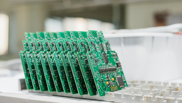
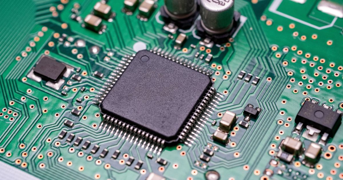
Europe’s electronics industry relies heavily on reliable PCB manufacturing Europe services to support sectors like automotive, aerospace, and medical devices. PCB manufacturing Europe stands out for strict quality compliance and advanced technical capabilities, but also faces unique challenges such as cost pressures and supply chain fragmentation. High-caliber European PCB manufacturers address these regional pain points by integrating optimized processes and collaborative supply chain strategies to deliver tailored solutions.

Top 15 PCB Manufacturing Companies in Europe(EU)
| Company Name | Country/Region | Main Business | Core Advantages | Process Capability | Lead Time |
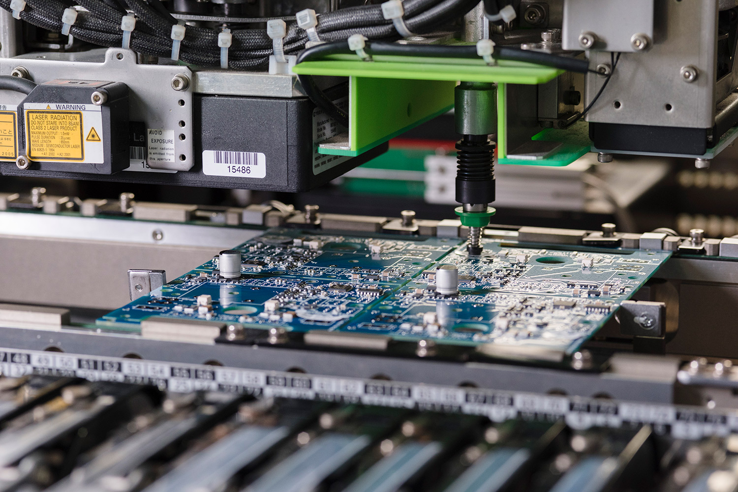
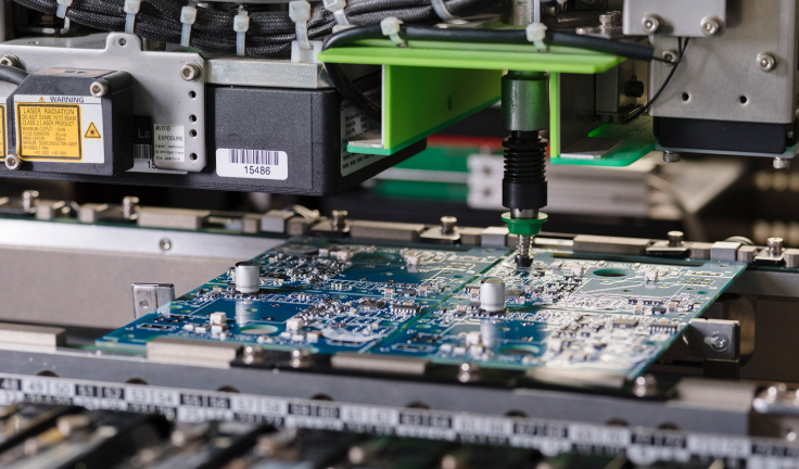
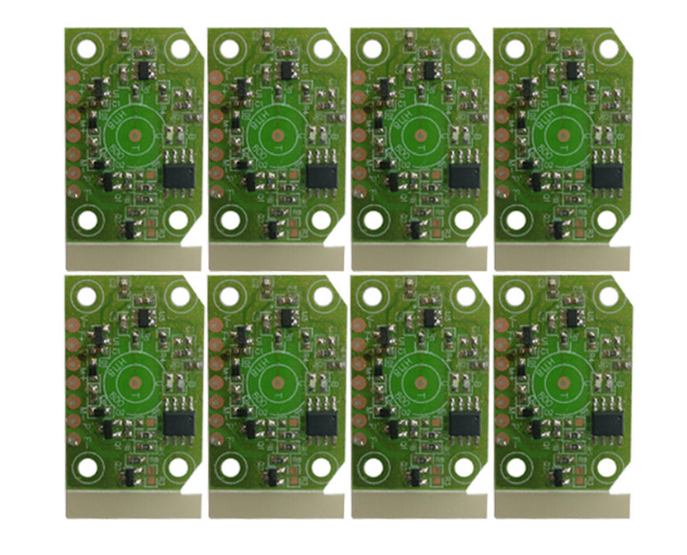
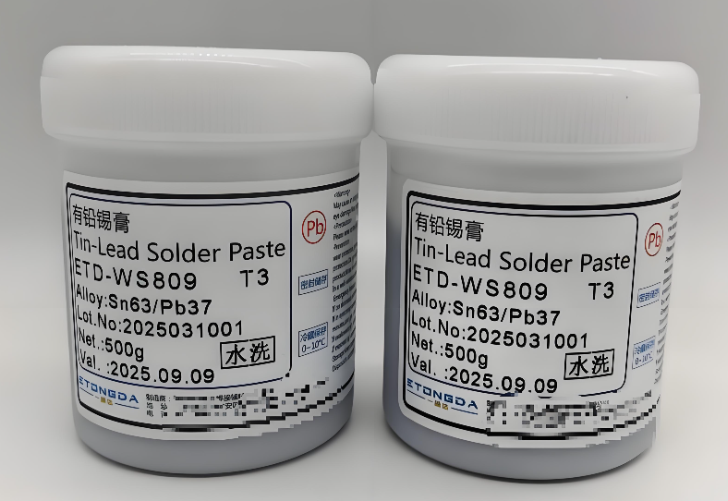
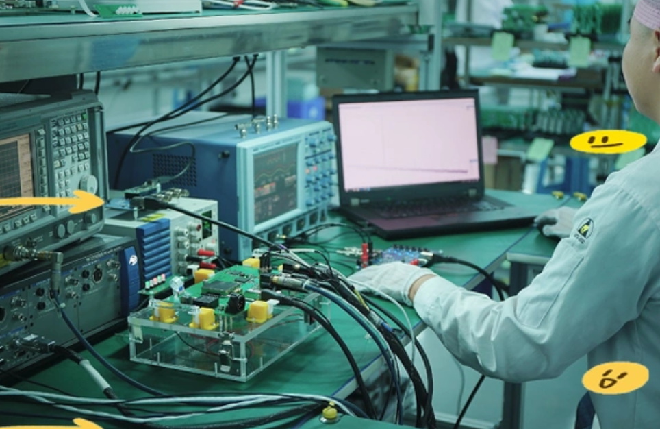
| Best Technology Circuit Co., Limited (EBest Circuit Co., Limited) | China (EU-compliant service) | Full-range PCB manufacturing (prototyping to mass production) & assembly for European markets | EU RoHS/REACH compliance, multilingual technical support, European distributor network | 2-32 layers, HDI, rigid-flex PCBs, impedance control, RF/automotive-grade production | Prototypes: 2-5 days; Mass production: 7-15 days; Expedited for EU clients |
| Eurocircuits | Germany/Hungary | Prototype & small-batch PCB manufacturing | Online data verification, cost-saving pooling service, local EU production bases | 2-16 layers, HDI microvias, RF PCBs, IPC-compliant production | Bare boards: 3-5 days; Assembled PCBs: 6-17 days |
| Zollner Elektronik | Germany | High-reliability PCB assembly for automotive/medical sectors | ISO 13485 certification, IATF 16494 compliance, complex assembly expertise | High-density assemblies, BGA/QFN soldering, cleanroom production | 10-20 business days |
| Enics | Switzerland | Industrial IoT & complex PCB assemblies | Localized EU production, sustainability focus, ISO 14001 certification | Rigid-flex PCBs, functional testing, high-temperature materials | 7-18 days |
| All Circuits | France | Aerospace/automotive PCB manufacturing & assembly | AS9100 aerospace certification, turnkey solutions, EU supply chain integration | High-reliability PCBs, thermal management, complex interconnect designs | 8-22 days |
| Ashgill Electronics | UK | Fast prototype PCB manufacturing | DFM support, low MOQ, UK local production | 2-8 layers, prototype assemblies, SMT technology | Prototypes: 3-7 days |
| Note AB | Sweden | OEM EMS & industrial PCB production | Large-volume production, quality traceability, Nordic quality standards | Standard/custom PCBs, industrial-grade material compatibility | 12-25 days |
| Kimball Electronics | Poland | IoT/medtech PCB manufacturing | ISO 13485 compliance, component sourcing support, Central EU logistics | Precision assemblies, cleanroom production, IoT-specific PCBs | 9-18 days |
| Neways Electronics | Netherlands | Automotive/healthcare PCB assemblies | RoHS compliance, long-term supply partnerships, Dutch quality control | 2-12 layers, power PCBs, high-current designs | 10-20 days |
| BMK Group | Germany | Mid-volume high-end PCB assembly | Aerospace certification, flexible production, German engineering precision | Complex PCBs, edge plating, high-precision drilling | 7-16 days |
| Asteelflash | France/UK | PCB manufacturing & box builds | EU supply chain, comprehensive testing, multi-site production | SMT assembly, functional testing, system-level integration | 8-20 days |
| Hanza Group | Sweden | Localized PCB production | Sustainability focus, regional logistics efficiency, Nordic environmental standards | Standard PCBs, small-batch assembly, lead-free manufacturing | 11-23 days |
| Videoton | Hungary | Consumer electronics PCB manufacturing | Cost-efficient large-scale production, Eastern EU manufacturing advantage | 2-10 layers, SMT assembly, high-volume fabrication | 10-18 days |
| Plexus | Romania | High-complexity PCB assemblies | Medical/industrial focus, strict quality control, EU regulatory compliance | HDI, BGA rework, complex component placement | 9-21 days |
| Scanfil | Finland | Industrial/renewable energy PCBs | Nordic quality standards, custom solutions, renewable energy expertise | Rigid PCBs, system assembly, high-voltage production | 12-24 days |
Which Manufacturers Offer Fast PCB Manufacturing Europe?
- EBest Circuit(Best Technology Circuit): Offers fast European PCB manufacturing services with a 2-5 day prototyping cycle and expedited mass production services. The company utilizes a global supply chain integrated with European distributors to ensure timely delivery while complying with EU regulations.
- Eurocircuits: Provides 3-day bare board prototyping and 6-day assembled PCB services for urgent orders, with online data verification and local European production facilities to accelerate turnaround times.
- Ashgill Electronics: Offers localized rapid prototyping services in the UK, with a 3-day turnaround time for simple designs, and provides DFM (Design for Manufacturability) support to streamline the iteration process while maintaining speed.
- Proto-Electronics: Provides instant online quotes and 5-15 day delivery times, offering fast European PCB manufacturing and assembly services, focusing on small-batch urgent orders and providing flexible order adjustment options.
- BMK Group: Offers high-end expedited PCB services for complex designs in 7-10 days, combining German engineering precision with flexible production planning to meet tight deadlines.
- Eurocircuits: Provides 3-day bare board prototyping and 6-day assembled PCB services for urgent orders, with online data verification and local European production facilities to accelerate turnaround times.
Types of PCB Manufacturing Europe(EU)
- Single sided and double sided PCB manufacturing.
- Multilayer PCB manufacturing Europe.
- HDI and microvia PCB production.
- Rigid flex and flex PCB fabrication.
- High frequency and impedance controlled PCB.
- Prototype and low volume PCB production.
- PCB manufacturing and assembly Europe.

How to Choose the Best PCB Manufacturer Europe?
Selection Guide to the Best PCB Manufacturer Europe:
- Thoroughly Verify EU Compliance Certification: First, confirm basic RoHS and REACH compliance. For specific industry needs, check IATF 164949 certification for automotive applications, ISO 13485 certification for medical devices, and AS9100 certification for aerospace projects. Require suppliers to provide complete compliance documents and material traceability reports to avoid market access risks.
- Precisely Match Technical Capabilities with Requirements: Based on product characteristics, accurately assess the supplier’s process capabilities. For high-frequency and high-speed products, focus on impedance control accuracy and HVLP4 copper foil compatibility. For complex structures, prioritize HDI micro-via and rigid-flex technologies. Evaluate DFM support and simulation tools to ensure design manufacturability and cost-effectiveness.
- Assess Supply Chain Risk Mitigation Capabilities: Given the shortage of high-end fiberglass cloth and high-frequency copper foil, check the supplier’s core material reserves, alternative material solutions, and the stability of cooperation with local European distributors. Prioritize manufacturers with dual material supply mechanisms to prevent production interruptions.
- Control Full-Process Quality Management: In addition to ISO 9001 certification, understand key testing processes, including X-ray inspection, flying probe testing, and thermal cycling testing. Require a batch traceability system and defect rate statistics to ensure quality consistency meets IPC-A-600 and IPC-A-610 standards.
- Balance Delivery Efficiency and Flexibility: Clearly define standard delivery times for prototypes (3-7 days) and mass production (7-20 days). Verify the ability to handle urgent orders. Prioritize PCB manufacturers with multiple production bases or local presence in Europe to shorten cross-border logistics cycles and address supply chain fragmentation issues.
- Calculate Total Life Cycle Cost Components: In addition to the unit price, break down logistics costs, customs duties, waste disposal costs, and compliance fees. Evaluate the supplier’s energy-saving processes to cope with rising European energy prices and avoid the accumulation of hidden costs. Confirm quotation transparency and price adjustment mechanisms.
- Consider Localized Service Support: Prioritize suppliers that provide multilingual technical support and local response teams for efficient design communication and problem-solving. Check after-sales service guarantees, including defective product repair processes, technical consultation response times, and long-term technical iteration support.
- Focus on sustainability and compliance upgrades: Verify ISO 14001 environmental certification and carbon footprint reporting. Evaluate green manufacturing processes, such as lead-free technology and waste recycling. Understand suppliers’ plans to adapt to future EU environmental regulations to ensure long-term collaborative compliance.
Quality Standards for PCB Manufacturing Europe
- RoHS Directive: Restricts hazardous substances (lead, cadmium) in PCB production.
- ISO 9001: Quality management system certification for consistent production.
- IATF 16949: Specific standard for automotive PCB manufacturing and assembly.
- ISO 13485: Compliance requirement for medical device PCB components.
- IPC-A-600: Acceptability criteria for bare printed boards.
- IPC-A-610: Standards for electronic assembly quality.
- REACH Regulation: Controls chemical substances used in PCB materials.
How to Verify the Technical Capability of PCB Manufacturer Europe(EU)?
Evaluation Guide to Technical Capability of PCB Manufacturer Europe(EU):
- Verify maximum layer count and HDI performance: Top European PCB manufacturers support up to 32 layers for rigid PCBs and 20 layers for HDI boards. HDI capabilities should include microvias as small as 0.1mm, blind/buried vias with aspect ratio 1:1, and mass production yield above 98% for such structures.
- Assess impedance control precision: For high-frequency applications (up to 40GHz), ensure impedance tolerance is within ±5% for characteristic impedances (50Ω, 75Ω, 100Ω). Advanced factories use automated impedance calibration tools with repeatability error below 0.5Ω.
- Evaluate material range and specifications: Confirm compatibility with EU standards, covering FR-4 (Tg≥170℃), polyimide (operating temperature -55℃ to 200℃), and metal core PCBs with thermal conductivity 1-4W/(m·K). Require material certificates for RoHS/REACH compliance.
- Check DFM support and simulation capabilities: Prioritize factories offering DFM reports within 24 hours, with simulation tools covering signal integrity (SI) and thermal analysis. Ensure support for optimizing designs to reduce production costs by 10%-15%.
- Review testing capabilities with quantitative indicators: Verify flying probe testing precision up to ±2μm, X-ray inspection for solder joints as small as 0.05mm, and functional testing with 99.9% test coverage. 4-8 probe parallel testing systems can improve efficiency by 2-4 times.
- Assess industry-specific project experience: For automotive/medical/aerospace sectors, require at least 5 years of mass production experience and 100+ qualified clients. Medical PCB manufacturers should have ISO 13485 certification with defect rates below 500ppm.
- Verify R&D investment and innovation output: Leading European PCB manufacturing facilities allocate 5%-8% of annual revenue to R&D. Check for 2-3 new patents per year related to HDI, material compatibility or testing technology.
- Check minimum line width and spacing accuracy: High-end factories achieve 9/12μm (line width/space) for fine-pitch designs, with batch consistency error within ±1μm. This is critical for compact IoT and automotive electronics.
- Evaluate surface treatment process stability: Support mainstream processes like ENIG (nickel layer 2-5μm, gold layer 0.05-0.1μm), OSP and immersion tin. Ensure corrosion resistance meets IPC-4552 standards, with salt spray test pass rate 100% for 48 hours.
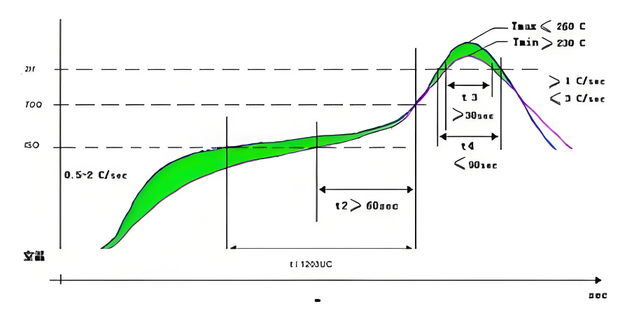
- Assess special process adaptability: For RF and automotive PCBs, confirm capability of controlled impedance routing (up to 100GHz) and thermal cycle testing (500+ cycles at -40℃ to 125℃) with no delamination.
How to Evaluate the Production Capacity of PCB Factory in Europe?
Evaluation Guide to Production Capacity of PCB Factory in Europe:
- Confirm monthly production capacity and scalability: For medium to large European PCB manufacturers, verify monthly capacity ranges from 50000 to 200000 square feet for rigid PCBs. Assess scalability by checking if they can boost output by 20 percent within 4 to 8 weeks without compromising quality.
- Evaluate lead time consistency and OTIF rate: Require an on-time in-full delivery rate of at least 95 percent for mass production orders. Review the past six months delivery reports to confirm lead time fluctuation is within ±1 day for standard batches.
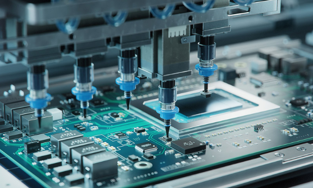
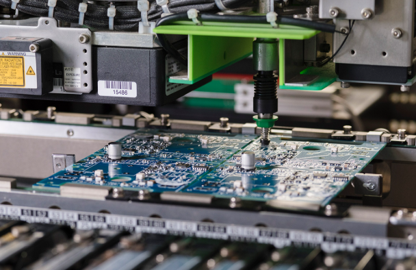
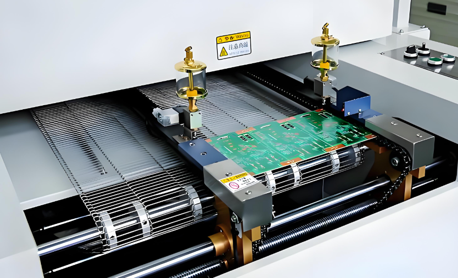
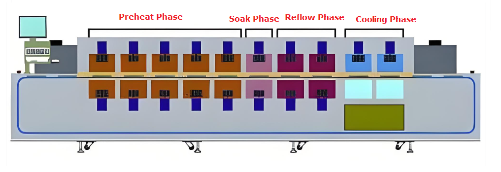
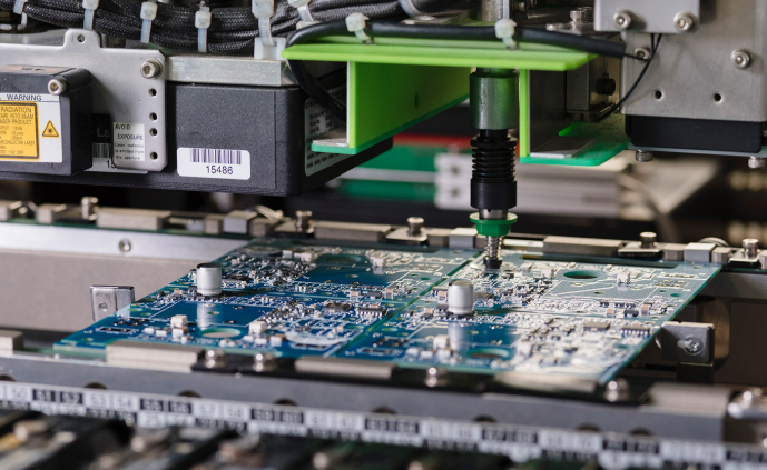
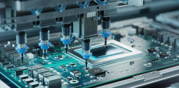
- Assess automation level and process stability: Check SMT production line automation rate of over 90 percent, equipped with robotic assembly and AOI SPI inspection. Verify MES systems monitor 120+ process parameters with automatic adjustments for deviations like etching temperature.
- Validate supply chain resilience for raw materials: Ensure core materials such as FR-4 and copper foil have dual source suppliers. Confirm key material inventory can cover 30+ days of production and cooperation stability with European local distributors.
- Verify batch traceability system completeness: Ensure traceability covers raw material batches production processes and final shipment. The system should provide full data retrieval within 24 hours, meeting EU compliance and quality control requirements.
- Check low-volume high-mix production flexibility: Assess changeover time for different PCB models modular equipment supports 15-minute switch for four-layer boards. Confirm capability to handle 8 to 12 mixed designs simultaneously with MOQ as low as 10 units.
Future Challenges of European PCB Manufacturers
- Escalating energy costs across Europe impacting production profitability.
- Growing competition from low-cost Asian manufacturers for mass production orders.
- Rapidly evolving technology requiring continuous investment in equipment and skills.
- Stricter EU environmental regulations increasing compliance costs and complexity.
- Component shortages and supply chain disruptions affecting production schedules.
- Skill gaps in the workforce for advanced PCB manufacturing Europe technologies.
- Pressure to adopt sustainable materials and circular economy practices.
- Geopolitical tensions disrupting cross-border supply and export opportunities.
FAQs of European PCB Manufacturing
Q1: How to reduce costs for low-volume PCB prototyping without sacrificing quality in Europe?
A1: Optimize for European PCB manufacturers offering pooling services to combine small-batch orders, cutting per-unit costs by 15%-20%. Leverage DFM analysis within 24 hours to optimize design (e.g., standardize hole sizes, reduce unique materials) and avoid rework. Prioritize local factories to eliminate cross-border logistics fees, while ensuring compliance with IPC-A-600 standards.
Q2: Why do high-frequency PCB prototypes often have signal integrity issues, and how to resolve them?
A2: Issues typically stem from improper trace routing, material mismatch, or impedance deviation. Choose low-loss dielectrics (e.g., FR-4 with Tg≥170℃) and control impedance tolerance within ±5% for 50Ω/75Ω lines. Use automated impedance calibration tools and SI simulation during design, and conduct RF testing post-production to identify signal loss, ensuring compatibility with high-frequency applications up to 40GHz.
Q3: How to handle last-minute component shortages during PCB assembly in Europe?
A3: Partner with suppliers having dual-source material mechanisms and a verified database of European distributors. Request alternative component suggestions with equivalent electrical performance, and ensure 24-hour verification of substitute parts. Opt for PCB manufacturing and assembly Europe services with local component inventory, which can reduce delivery delays by 30% compared to global sourcing.
Q4: What causes BGA soldering defects in European PCB assembly, and how to prevent them?
A4: Common causes include inadequate stencil alignment, improper reflow temperature profiles, and board warpage. Use automated stencil printing and AOI/SPI inspection to ensure alignment accuracy within ±2μm. Calibrate reflow ovens to match component specifications, and conduct X-ray inspection for hidden solder joints. Choose factories with SMT automation rates over 90% to minimize human error.
Q5: How to obtain complete compliance documentation for PCBs sold across the EU?
A5: Request a standardized compliance package from suppliers, including RoHS/REACH test reports, material certificates, and batch traceability records. Ensure suppliers integrate compliance checks into production processes, with real-time data retrieval within 24 hours. For medical/automotive PCBs, additional ISO 13485/IATF 16949 certification documents are required to meet sector-specific regulations.