Modern lighting technology has evolved rapidly. Engineers now have many LED packaging options. Among them, COB and CSP LEDs attract significant attention. These two technologies power many lighting products today. You can find them in automotive lights, flashlights, commercial lighting, and plant grow systems.
However, designers often ask the same question: COB vs CSP LED — which one is better for a project? In this guide, you will know the answer.
What Is COB LED and How Does It Work?
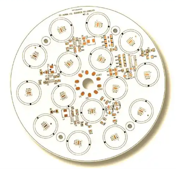
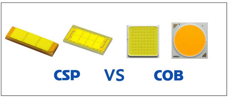
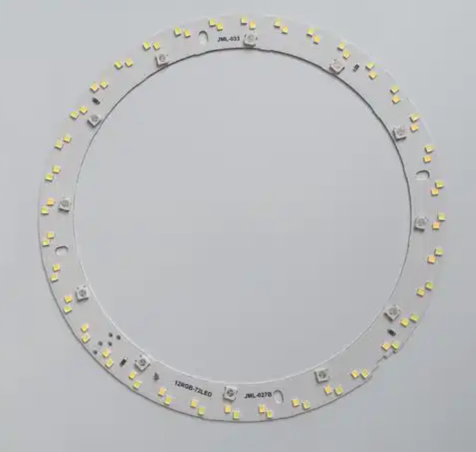
COB means Chip on Board, in this packaging method, multiple LED chips are mounted directly onto a single substrate. The chips operate together as one large light source.
A phosphor layer usually covers the chip array to produce uniform white light. Because many chips sit close together, a COB module behaves like a single powerful emitter.
A typical COB structure includes:
- LED chips mounted directly on the board
- Bonding wires connecting chips
- Phosphor coating for light conversion
- Thermal interface with a metal-core PCB
The result is a powerful and stable lighting module that delivers high brightness with smooth illumination.
This structure offers several advantages.
- High luminous density
- Smooth and uniform light output
- Compact light source
- Good thermal path through the substrate
Because the chips sit close together, a COB module behaves like a single high-power LED emitter. This makes it popular for applications that require strong and uniform illumination.
Typical COB Applications
- High bay lighting
- Spotlights
- Downlights
- Studio lighting
- Automotive headlights
What Is CSP LED and How Is It Different from COB?
CSP stands for Chip Scale Package. Unlike traditional LED packaging, CSP LEDs remove most of the external package structure, the LED chip itself acts as the package. In simple terms, a CSP LED is almost the same size as the LED die.
This minimal structure provides several advantages:
- Smaller footprint
- Lower thermal resistance
- Higher packing density
- Better optical efficiency
Because of this design, CSP LEDs can be mounted directly onto a PCB using standard SMT assembly processes. Compared with COB modules, CSP LEDs operate as individual light sources rather than one combined emitter. Designers often arrange multiple CSP LEDs across a PCB to achieve the desired brightness.
Applications of CSP LEDs
- Smartphone flash LEDs
- Automotive lighting
- LED strips
- Flashlights
- High-density lighting modules
What Is the Difference Between COB vs CSP LED?
Although both COB and CSP technologies use LED chips, their packaging methods differ significantly. The following table summarizes the main differences.
| Feature | COB LED | CSP LED |
| Packaging structure | Multiple chips integrated on board | Chip-scale package |
| Light source | Single uniform emitter | Multiple discrete emitters |
| Light uniformity | Very smooth | Slightly segmented |
| Efficiency | High | Very high |
| Size | Larger module | Very compact |
| Assembly method | Module mounting | SMT placement |
| Thermal management | Requires metal-core PCB | Requires efficient PCB cooling |
This difference affects several design factors:
- beam pattern
- thermal management
- manufacturing method
- PCB layout
For high-power lighting systems, engineers often choose COB modules. For compact lighting systems, CSP LEDs provide greater flexibility.
CSP vs COB: Which is Better?
Many designers ask: csp vs cob which is better? There is no universal answer. The better option depends on the product design and lighting requirements. Engineers often select technology based on thermal density and optical design.
If the product needs a smooth beam and powerful output, COB is often preferred. If the design requires many small emitters, CSP LEDs provide more flexibility. In practice, both technologies can achieve excellent results when paired with appropriate PCB materials and thermal design.
Which LED Technology Generates More Heat: COB or CSP?
Heat management is critical in LED systems, high temperatures reduce efficiency and shorten LED lifetime. Both COB and CSP LEDs generate heat, but their behavior differs.
COB modules place many chips in a small area, this creates high thermal density beneath the module. CSP LEDs distribute chips across the PCB, spreading heat more evenly.
| Thermal Aspect | COB LED | CSP LED |
| Heat density | High | Moderate |
| Thermal distribution | Localized | Distributed |
| Cooling demand | High | Moderate |
Because COB concentrates heat, it often requires metal-core PCBs for effective cooling.
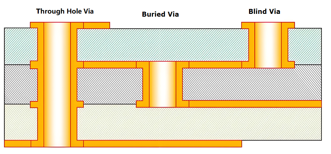
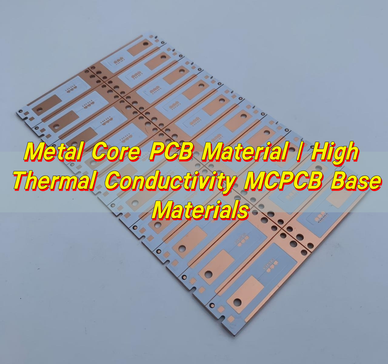
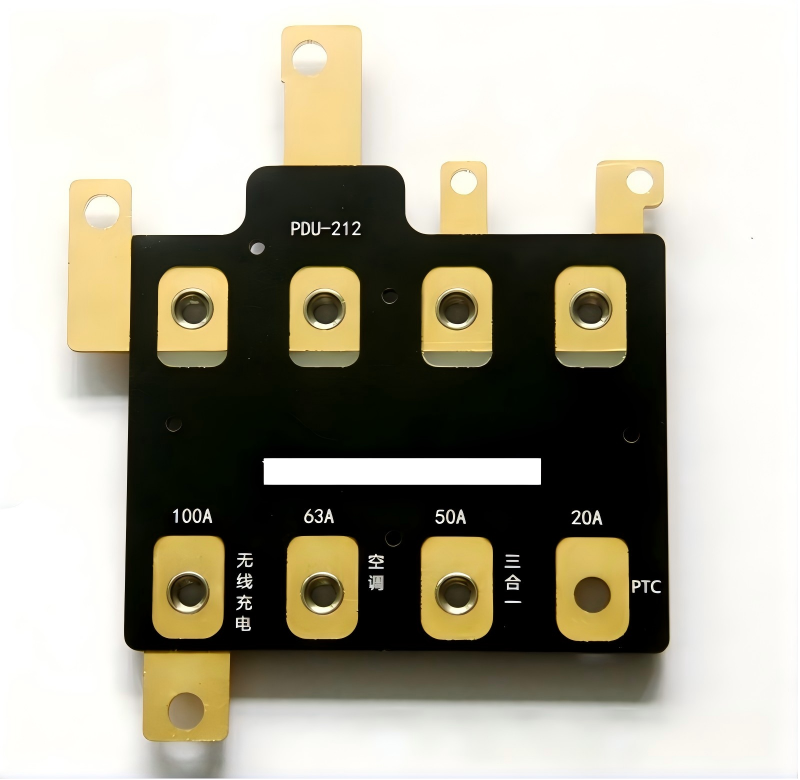
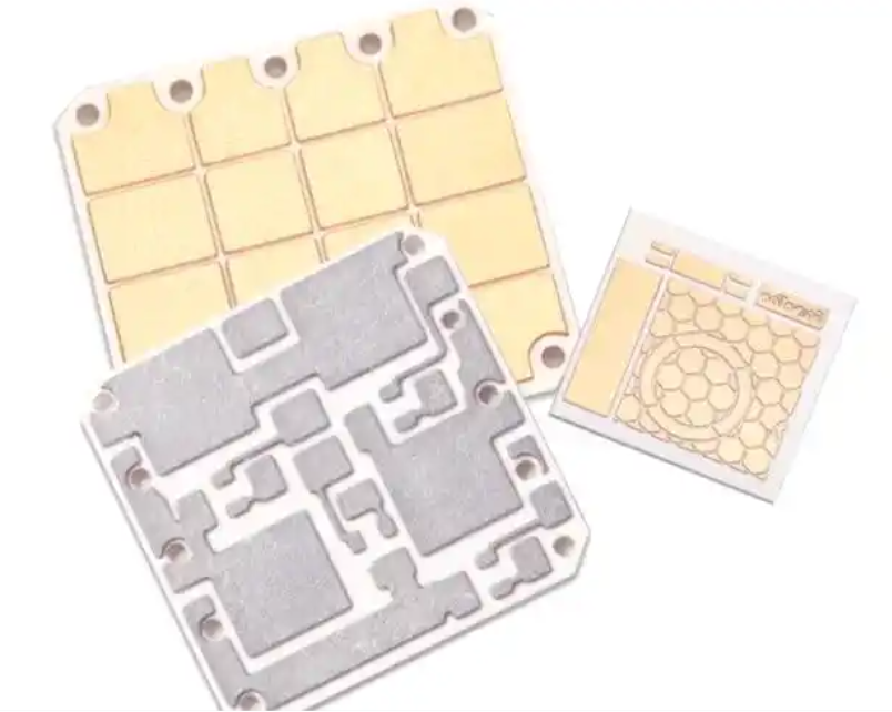
Why Do High-Power LEDs Use Aluminum PCB or Copper PCB?
Traditional FR4 circuit boards have limited thermal conductivity, their thermal conductivity typically ranges around 0.3 W/mK. High-power LEDs require better heat dissipation, excess heat reduces brightness and accelerates aging. This is why many LED systems use metal-core PCBs.
The most common options include:
- Aluminum PCB
- Copper PCB
These materials transfer heat away from the LED much faster than standard FR4 boards.
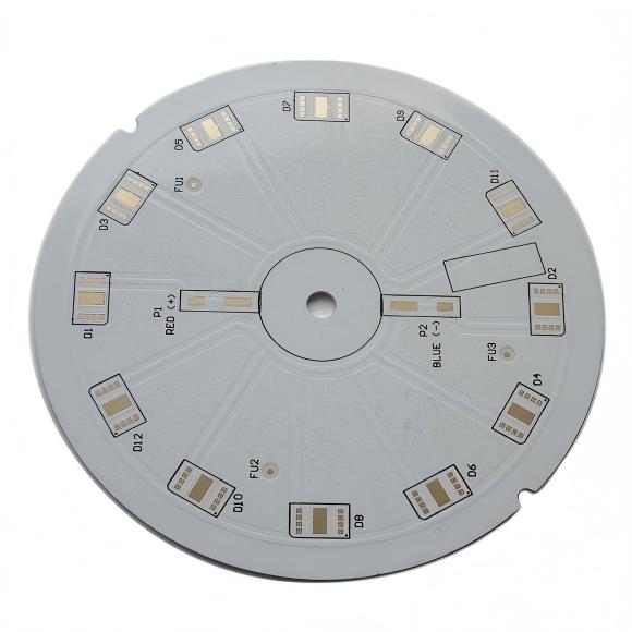
Aluminum PCBs are widely used in commercial lighting. They offer a balance between cost and performance. Copper PCBs provide even higher thermal conductivity. They are often used in:
- high-power LEDs
- automotive headlights
- industrial lighting
For both cob led vs csp led chips, metal-core PCBs greatly improve heat transfer.
How Does PCB Design Affect COB and CSP LED Performance?
PCB design strongly influences LED performance, even high-quality LED chips cannot perform well on poorly designed boards.
Several PCB factors affect COB and CSP LED performance:
- thermal path design
- copper thickness
- PCB material
- solder pad layout
For COB modules, the board must provide a strong thermal interface, aluminum core boards are commonly used.
For CSP LEDs, pad design is critical, each chip must transfer heat efficiently through the PCB.
A well-designed COB LED PCB layout helps maintain lower junction temperatures and stable output.
How to Choose the Right PCB for COB and CSP LED Projects?
When choosing the correct PCB material ensures long-term LED reliability, designers usually consider:
- LED power level
- heat density
- product size
- manufacturing cost
For many lighting systems, aluminum PCBs provide the best balance between cost and thermal performance.
Copper PCBs are often selected for high-power lighting where stronger heat dissipation is required. General guidelines include:
- COB lighting commonly uses aluminum PCBs
- Dense CSP arrays may benefit from copper PCBs
- Automotive LEDs often use copper boards
When evaluating csp vs cob which is better, the PCB thermal solution should always be considered.
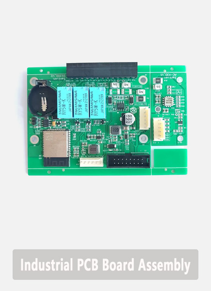
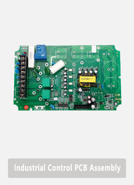
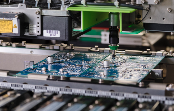
Partner with EBest Circuit for One-stop COB and CSP LED PCBs
EBest Circuit (Best Technology) supports manufacturers developing COB and CSP LED lighting products. With nearly twenty years of PCB manufacturing experience, our engineering team understands the thermal challenges of LED systems.
We provide integrated services including PCB fabrication, component sourcing, and assembly support. Our engineers also help customers optimize PCB layouts for better heat dissipation.
Key advantages include:
- Aluminum PCB and copper PCB manufacturing
- Engineering support for LED PCB design
- Fast PCB prototyping and production
- Integrated PCB and PCBA services
Our solutions help lighting manufacturers build reliable and efficient LED products. For PCB design consultation, prototyping, or full LED PCB manufacturing support, please feel free to contact: sales@bestpcbs.com