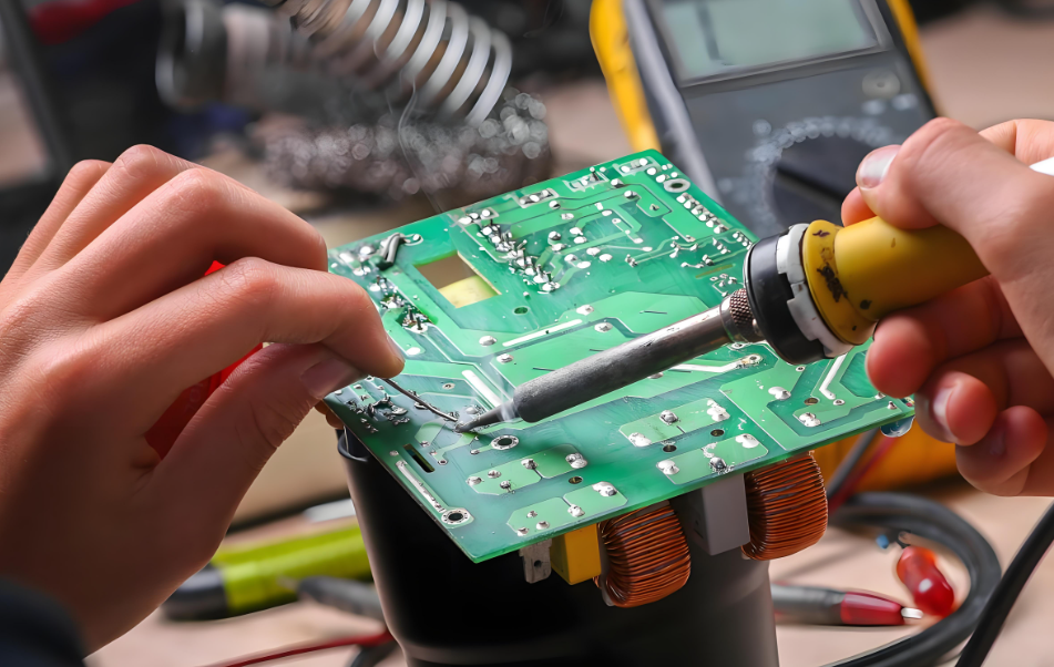
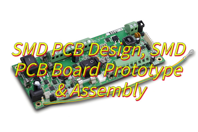
RFID PCB design is at the core of how RFID systems work. It controls how signals are sent, received, and interpreted. These systems are found in access cards, smart shelves, tracking systems, and countless other products. The rfid pcb needs to be carefully planned and built to ensure strong signal communication, stable frequency, and resistance to interference. This guide will walk you through the fundamentals, challenges, and design process — especially for rfid pcb antenna design including 125kHz rfid pcb antenna design.
RFID Definition
RFID stands for Radio Frequency Identification. It uses electromagnetic waves to transfer data between a tag and a reader. The tag contains a small chip and an antenna that stores information. When it enters the range of a reader, the antenna picks up the reader’s signal and sends back data.
RFID works across several frequency bands:
- Low Frequency (LF) – around 125kHz to 134.2kHz
- High Frequency (HF) – typically 13.56MHz
- Ultra-High Frequency (UHF) – 860MHz to 960MHz
- Microwave – around 2.45GHz
LF and HF are preferred for short-range applications like key fobs and access control. UHF is used for supply chain tracking, logistics, and retail due to its longer range.
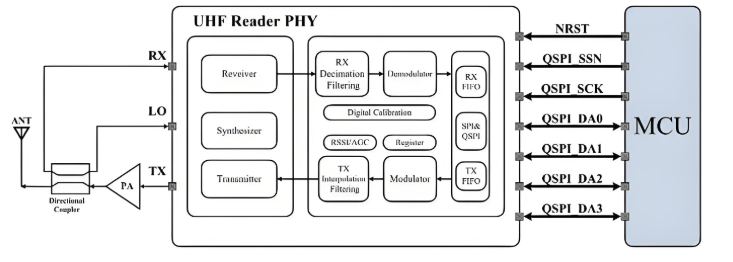
What Is RFID PCB?
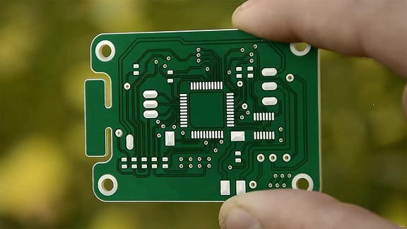
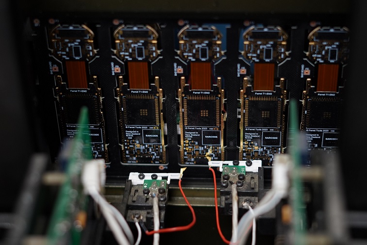
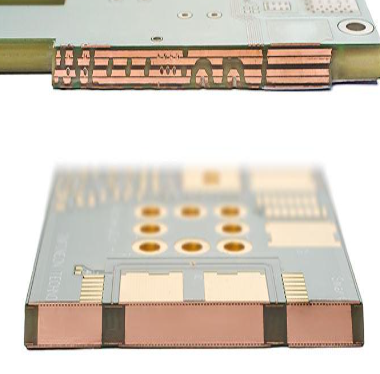
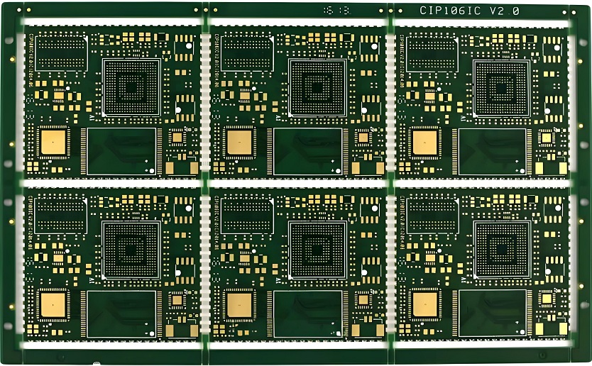
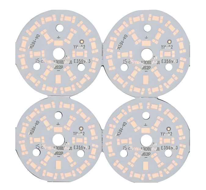
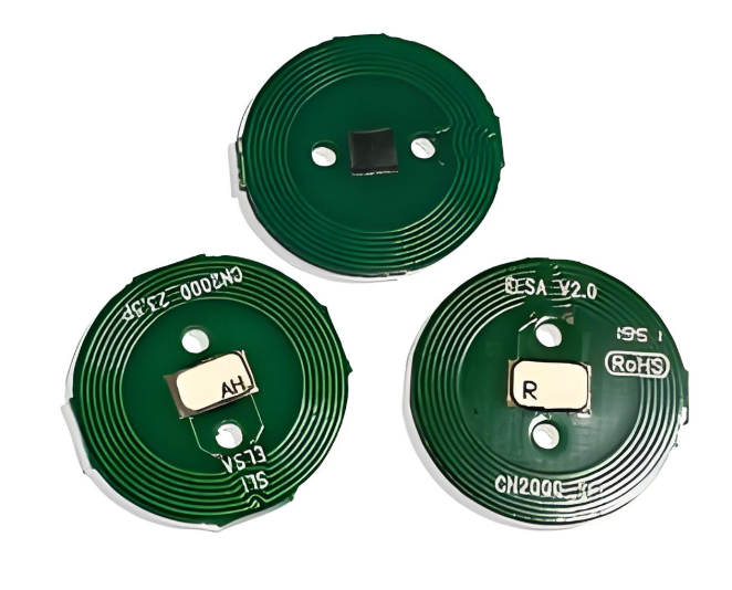
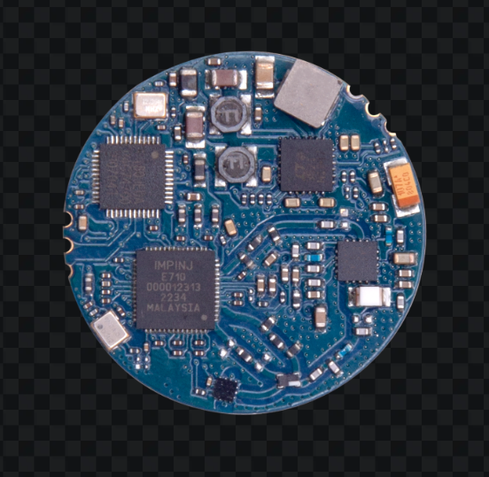
An RFID PCB is a custom-designed circuit board that integrates the antenna, IC chip, and sometimes power components into a single board. It forms the physical layer of the RFID system. The pcb hosts the antenna as a copper trace, connects it with the chip, and ensures signal performance across its frequency band.
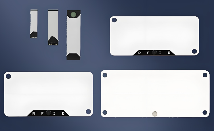
RFID PCBs are typically used in:
- Smart cards and access badges
- Animal tags and implants
- Supply chain and inventory tags
- Automotive immobilizers
- IoT sensors

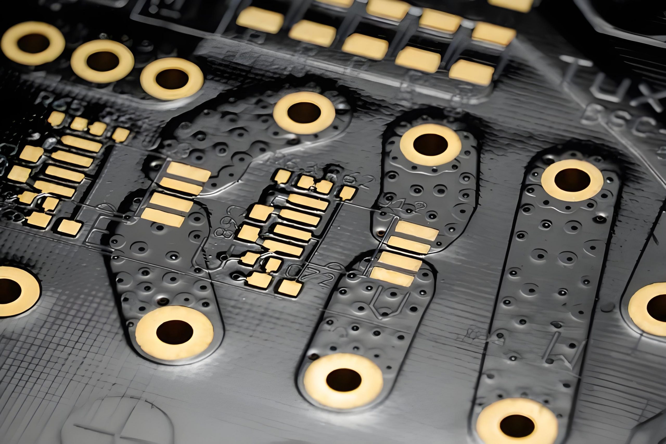
Unlike off-the-shelf PCBs, rfid pcbs require exact control of trace dimensions and substrate materials to function correctly.
Features of RFID PCB
Designing a good rfid pcb means balancing several performance and physical factors:
1. Compact Structure
Many RFID tags must be small. The PCB design should support a compact layout without losing signal quality.
2. Frequency Stability
RFID systems must operate at precise frequencies. PCB material and layout affect how stable these frequencies are over time and temperature changes.
3. Low Signal Loss
Every micro-ohm of resistance matters. Losses in the antenna trace or poor impedance matching can weaken the signal.
4. Durability
RFID PCBs may be embedded in plastic, metal, or other enclosures. They need to resist wear, vibration, and environmental changes.
5. High Sensitivity
A well-designed RFID PCB can detect weak signals from far away. This is especially critical for passive tags without their own power source.
What Materials Are Used in RFID PCB?
Material selection greatly influences the performance of rfid pcb antenna design. Let’s look at the most common options:
- FR4
FR4 is a standard fiberglass-reinforced laminate. It is affordable and widely used. For 125kHz rfid pcb antenna design, FR4 works well because signal loss is minimal at low frequency. However, it isn’t ideal for UHF or microwave designs due to its high dielectric loss.
- Rogers Materials (RO3003, RO4350B)
Rogers materials are engineered for high-frequency use. They provide low dielectric loss and tight control over Dk values, which helps maintain signal integrity in UHF and HF RFID PCBs.
- Ceramic-Filled PTFE
This material has ultra-low loss, high precision, and excellent thermal stability. It’s perfect for performance-critical applications like aerospace or medical RFID tags but is more expensive.
- Flexible Substrates (Polyimide)
Used in wearable or curved applications, flex PCBs can integrate antennas into compact or irregular shapes. Though harder to manufacture, they offer design freedom.
RFID PCB Design Basics
Designing an RFID PCB demands precision, especially at high or ultra-high frequencies. The primary objective is to maintain signal integrity while minimizing interference and energy loss. The antenna and circuit layout should align precisely with the target frequency, which varies by RFID system (LF, HF, or UHF).
In LF (125kHz) systems, the antenna is typically a spiral coil. For HF (13.56MHz), designs also employ loop antennas, whereas UHF (860–960MHz) systems utilize dipole or patch antennas. Each configuration demands specific impedance control and matching techniques to prevent signal reflection and power loss.
The trace geometry—including width, spacing, and number of turns—must be accurately calculated to meet inductance requirements. Additionally, impedance matching networks are often used to align the antenna’s impedance with the RFID chip, improving signal transmission.
Effective grounding, shielding, and material selection also play key roles in suppressing noise and reducing parasitic effects. Simulations using tools like CST or HFSS are highly recommended to validate the design before manufacturing.
Design Considerations of RFID PCB Antenna
Designing an RFID antenna on a PCB is not just about drawing coils or traces. It’s about creating a reliable RF communication path. The key considerations include:
1. Operating Environment
Materials around the antenna—plastic casings, metal enclosures, or even human skin—can detune the antenna. You should simulate the antenna in the actual environment or enclosure where it will operate.
2. Antenna Location and Orientation
The tag must align well with the reader’s signal field. Poor placement can drastically reduce range. Keep the antenna away from large ground planes, which can absorb or reflect RF signals.
3. Tuning and Matching
Each antenna must be tuned to its target frequency, considering the inductance and capacitance of the layout. For low-frequency RFID (like 125kHz), this is often done with tuning capacitors. For UHF, tuning is more complex and may involve impedance-matching networks.
4. Board Stackup and Dielectric Properties
The thickness and material of the board influence antenna behavior. Thicker boards or high-Dk materials can introduce parasitic effects. Keeping the substrate consistent during design and production is critical.
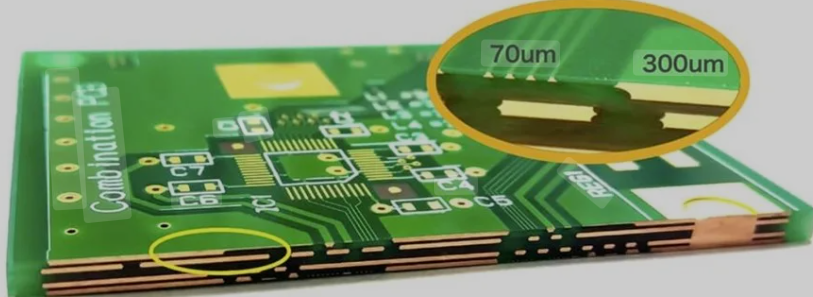
5. Copper Thickness and Trace Width
These determine the Q factor (quality factor) of the antenna. A higher Q results in better sensitivity but may reduce bandwidth. Carefully select the copper weight and trace dimensions during layout.
6. Component Integration
If other components are placed near the antenna—like batteries, sensors, or shielding cans—they may interfere with signal quality. Use ground planes wisely and add clearance where possible.
125kHz RFID PCB Antenna Design
Designing a 125kHz RFID PCB antenna requires a deep understanding of magnetic field coupling and low-frequency circuit behavior. Unlike higher-frequency RFID systems that rely on far-field electromagnetic waves, 125kHz systems operate using near-field inductive coupling. This means that the strength and orientation of the magnetic field directly influence performance.
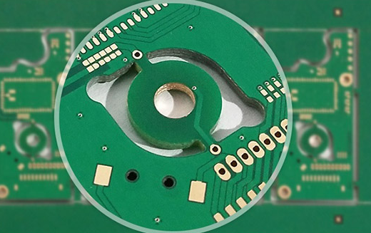
The antenna in this case is a spiral inductor, typically etched onto a single or double-layer PCB. The number of turns, spacing between traces, trace width, and board size determine the inductance. A common design goal is to achieve an inductance of around 100–500μH, depending on the application.
Resonance tuning is accomplished by placing a parallel capacitor with the coil, calculated using the formula:

This forms a resonant LC circuit tuned precisely to 125kHz. The Q factor of the antenna, which measures the sharpness of resonance, is influenced by the coil resistance and inductance. A higher Q yields better sensitivity but may reduce tolerance to detuning.
Additional considerations include minimizing EMI, optimizing layout symmetry, and keeping the antenna away from ground pours and metal housings. Since many applications use 125kHz for secure access, pet tracking, or vehicle immobilizers, reliability and consistency are critical.
What Is the Major Problem With RFID PCB?
The main challenge in rfid pcb design is interference. Radio signals are easily disrupted by nearby metals, improper grounding, or poor layout.
Here are some common problems:
- Antenna detuning when embedded in plastic or placed next to metal parts
- Weak signal strength due to poor impedance matching
- Manufacturing defects like uneven trace widths or delamination
- Environmental changes like moisture or heat affecting substrate dielectric properties
- Limited range if tuning is off or the antenna is too small
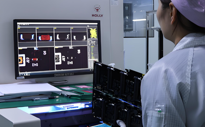
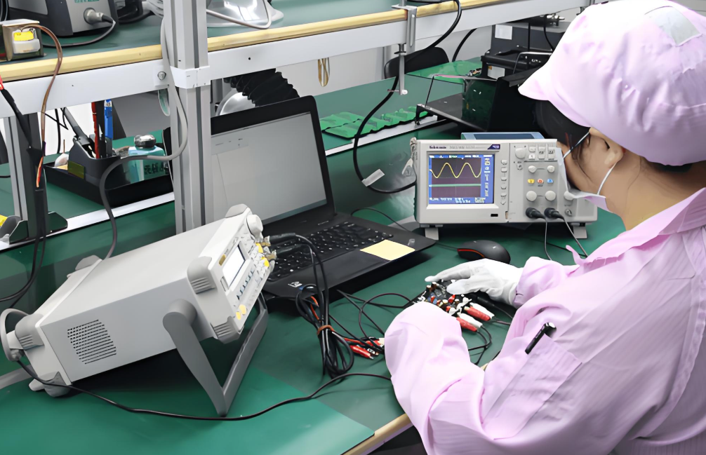
These issues can be fixed early in the design process with simulation, testing, and material control.
Conclusion
The success of any RFID system heavily depends on good rfid pcb design. It’s not just about drawing traces — it’s about understanding materials, signal behavior, and antenna principles. Whether you’re working with 125kHz rfid pcb antenna design or designing a UHF RFID tracker, every decision you make on the PCB matters.
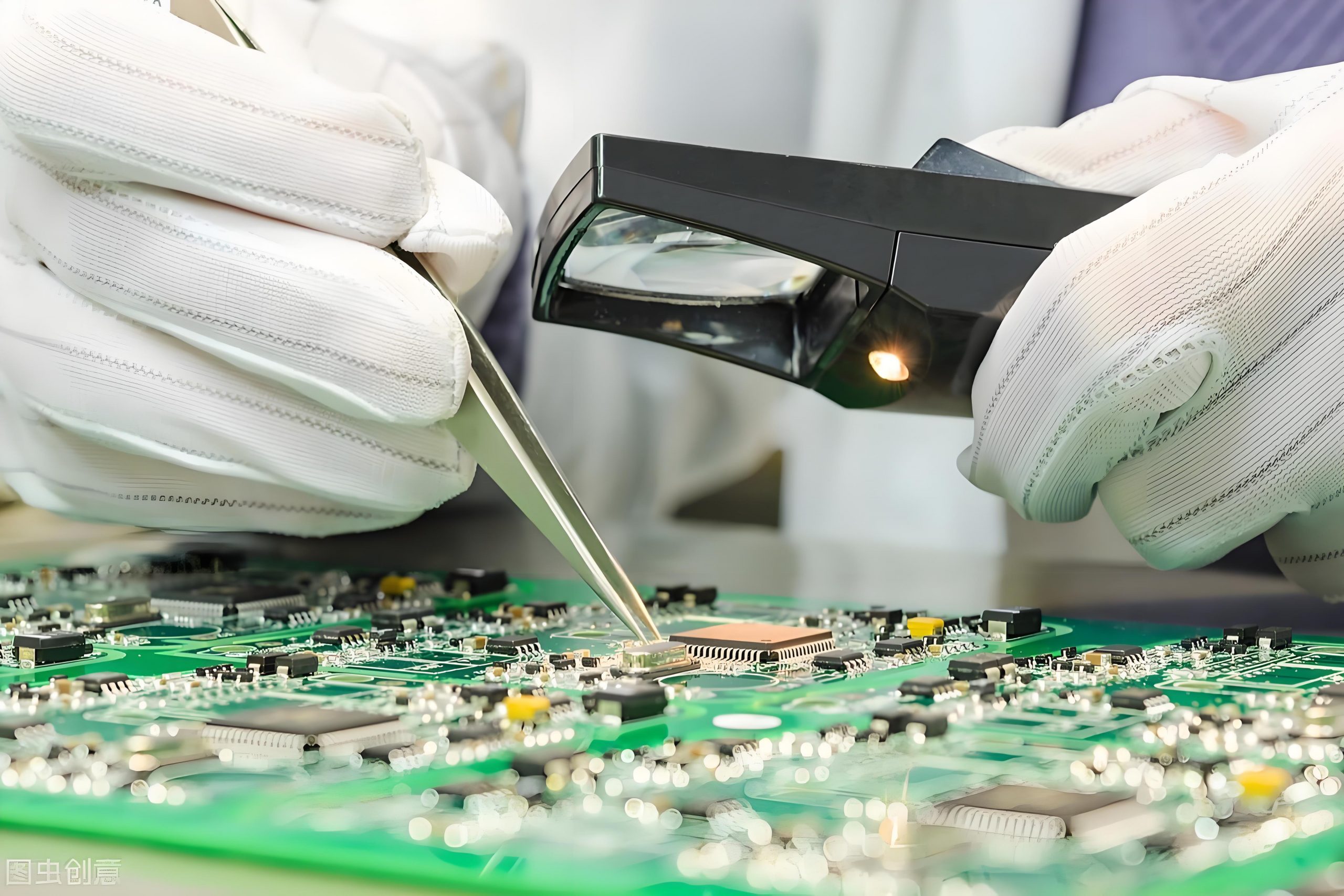
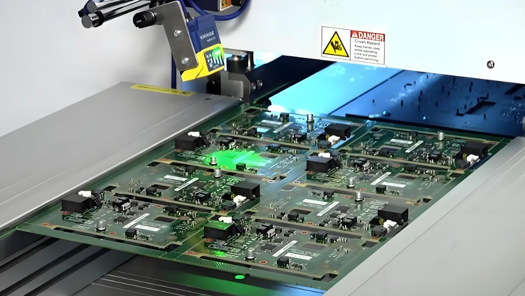
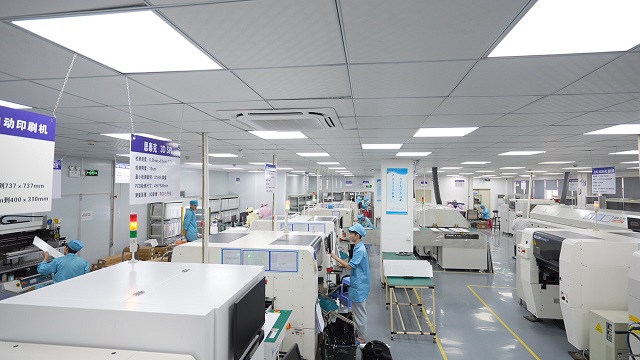
At EBest Circuit (Best Technology), we provide full RFID PCB solutions — from layout and simulation to prototyping and mass production. We work with both standard and advanced materials and follow strict quality systems to deliver reliable, high-performance PCBs.
FAQs
1. What is the typical range of a 125kHz RFID tag?
It usually ranges between 5 to 15 cm, depending on coil size, power, and environmental factors.
2. Can I use the same RFID PCB for different frequencies?
No. RFID PCBs must be designed specifically for the target frequency due to antenna size and material constraints.
3. How do I improve RFID read range?
Use a larger antenna, optimize impedance matching, and choose low-loss materials. Avoid placing the antenna near metal objects.
4. What’s better for RFID: FR4 or Rogers?
FR4 is cost-effective and fine for low-frequency tags. For UHF or precision applications, Rogers is a better choice due to lower dielectric loss.
5. Can EBest Circuit (Best Technology) help with RFID prototyping?
Yes! We offer complete support from antenna design, simulation, and prototyping to full-scale manufacturing with high precision and reliability.