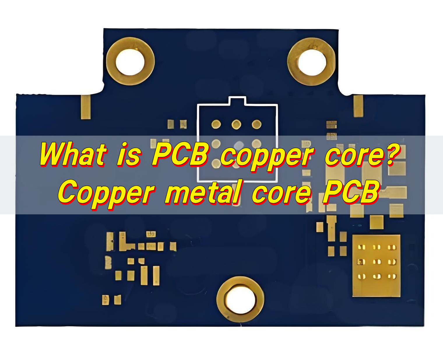
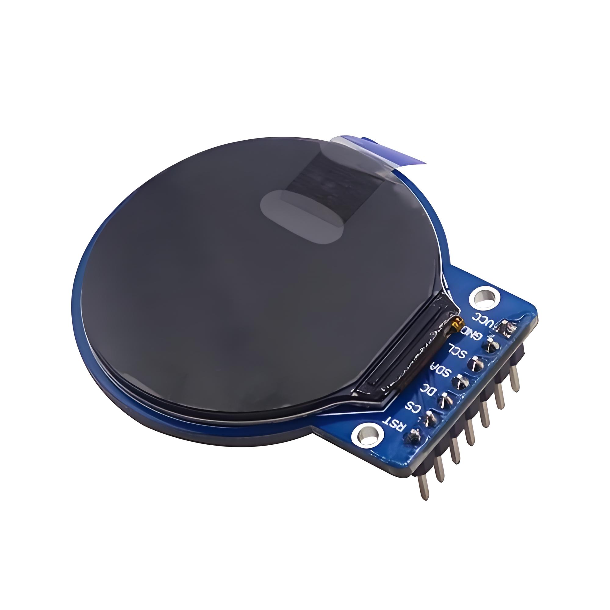
When you look at your smartphone, car navigation screen, or even a medical monitor, you’re looking through a TFT display. TFT, which stands for Thin Film Transistor, is a technology that allows precise control of millions of pixels, producing sharp images and vibrant colors. Yet, behind the glass layer of the display lies something equally important—the TFT PCB.
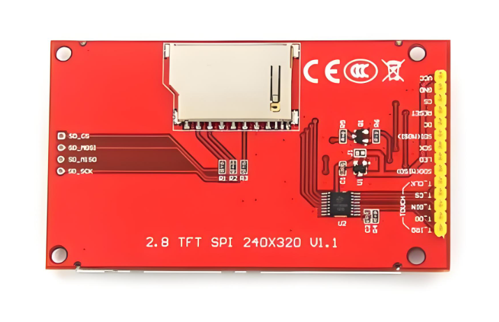
The TFT PCB is the printed circuit board that supports and controls the TFT display module. Without it, the panel is just passive glass, unable to light up or show an image. The PCB provides the “intelligence” that makes the display come alive. It manages signals, regulates power, drives the backlight, and often integrates the touch interface.
Understanding how TFT PCBs function is essential not only for engineers but also for product developers, purchasing managers, and anyone working with display modules. Let’s explore what a TFT PCB is, how it works, where it’s used, and why choosing the right manufacturing partner is vital.
What is a TFT PCB in a Display?
At its core, a TFT PCB is the electronic backbone of a TFT display module. The TFT display consists of two main parts:
- The TFT glass – This contains the thin film transistors that control liquid crystal molecules, determining how light passes through each pixel.
- The TFT PCB – This supports the TFT glass by supplying power, processing signals, and controlling the backlight.
Think of the TFT glass as the screen canvas, and the TFT PCB as the control center. The glass defines the resolution, pixel density, and visual quality, but without the PCB, there’s no way to convert system signals into images.
For example, a 7-inch automotive TFT screen may have a resolution of 1024×600. The TFT glass determines the number of pixels, but it’s the PCB that drives each of those pixels according to the instructions from the car’s mainboard.
How Does a TFT PCB Work?
The TFT PCB works like an interpreter between the system and the display. Its tasks can be divided into three major functions:
1. Signal Processing
The host device—whether a smartphone, industrial controller, or infotainment system—sends digital image data. But this data needs to be formatted into instructions that control each pixel.
- Signal Input: Common formats include LVDS, eDP, or MIPI DSI.
- Driver ICs: These chips on the PCB decode the signals and decide how each pixel should behave.
- Row and Column Control: Signals are distributed row by row and column by column, activating specific transistors on the TFT glass.
For example, when displaying a red dot in the corner of a smartphone screen, the PCB’s driver ICs calculate which pixels to energize and how to modulate them to show red.
2. Power and Backlight Management
TFT displays require several power rails: one for the logic, one for the glass, and one for the LED backlight.
- Voltage Regulation: The PCB includes regulators to maintain stable voltages, typically ranging from 1.8V for logic to 12V for backlight.
- Backlight Control: LED drivers adjust brightness through PWM (Pulse Width Modulation) or current control. This makes it possible to dim the screen for night use or boost brightness for outdoor visibility.
Without these circuits, the display would flicker, show unstable images, or fail to achieve uniform brightness.
3. Touch Controller Integration
In many TFT modules, the PCB also supports the touch layer.
- Capacitive Touch Controllers: Sense changes in capacitance when a finger touches the screen.
- Resistive Touch Controllers: Detect pressure applied on the surface.
The PCB processes these touch signals and communicates them back to the main system.
This is how swiping on your smartphone screen or tapping a medical device control panel is translated into action.
What are the Key Components on a TFT PCB?
Although the PCB looks small, it’s packed with vital parts. Let’s look at them in detail:
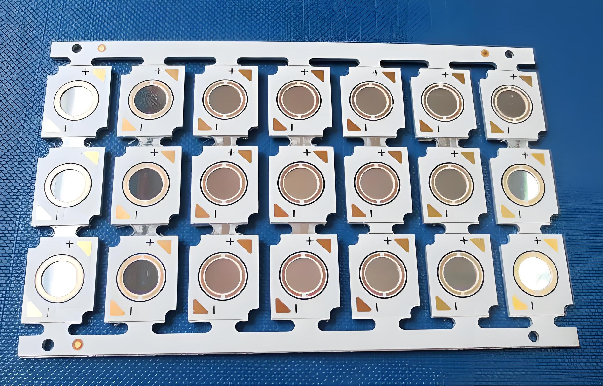
- Driver ICs: Often fine-pitch chips that directly control pixel rows and columns. They are critical for image sharpness and color accuracy.
- Power ICs: Convert input power into the different voltage levels needed by the display and touch controller.
- Backlight Circuitry: Includes LED drivers, current regulators, and protection circuits.
- Touch Controller: Only present in touch-enabled displays. Handles finger tracking, multi-touch, and gesture recognition.
- Connectors and FPCs: Provide the bridge between the PCB and the host system. For slim devices, flexible printed cables (FPCs) are widely used.
- Oscillators and Timing Circuits: Ensure that signals reach the glass in perfect sync.
In high-end automotive or medical displays, additional components may be added, such as temperature sensors, EMI filters, and redundant power circuits for safety.
What are the Applications of TFT PCBs?
TFT PCBs are used in nearly every industry where visual information is needed. Some of the most common applications include:
- Consumer electronics – Smartphones, tablets, laptops, TVs.
- Automotive – Digital dashboards, navigation systems, entertainment screens.
- Industrial equipment – Control panels, human-machine interfaces (HMIs).
- Medical devices – Patient monitors, diagnostic equipment.
- Aerospace and defense – Rugged displays with high visibility and durability.
In each application, the PCB is customized to meet specific requirements, whether it’s compact size, heat resistance, or EMI shielding.
What are the Design Considerations for TFT PCBs?
Designing a TFT PCB is more challenging than many other PCB types because of the high-speed signals, compact layouts, and strict reliability needs.
1. High-Speed Signal Integrity
TFT PCBs often carry LVDS, MIPI DSI, or eDP signals that run in the hundreds of megahertz.
- Impedance Control: Differential traces are routed with controlled impedance, usually 90 Ω ± 10%.
- Length Matching: Signal pairs are length-matched to avoid skew.
- Grounding and Shielding: Reference planes are carefully planned to minimize crosstalk.
2. Power Distribution and Stability
- Multiple Rails: A single TFT PCB may require 1.8V, 3.3V, 5V, and 12V simultaneously.
- Filtering: LC filters smooth power for sensitive circuits.
- Decoupling Capacitors: Placed close to ICs to reduce noise and voltage dips.
3. Thermal Management
- Backlight Heat: LED backlights generate heat. Copper pours, thermal vias, and sometimes aluminum-backed designs are used.
- IC Heat Dissipation: High-power driver ICs may need thermal pads to spread heat across the PCB.
4. Mechanical and Form Factor Constraints
- Thickness: Many handheld devices demand ultra-thin PCBs (as low as 0.4 mm).
- Flexibility: For foldable devices, the PCB must endure repeated bending.
- Mounting Holes: Carefully placed to avoid stress on the glass.
5. Reliability for Harsh Environments
- Automotive: Wide temperature (-40°C to 125°C), vibration-resistant designs.
- Medical: Compliance with strict safety standards, including isolation for patient-connected devices.
- Aerospace: Lightweight but highly reliable boards, often using advanced laminates.
6. Cost vs Performance
Every design choice affects cost.
- More Layers = better performance, higher cost.
- ENIG Finish = better for fine-pitch, but more expensive than OSP.
- Hybrid Rigid-Flex PCB = saves space, but increases production difficulty.
Example: A simple home appliance TFT PCB may use a 2-layer OSP-finished board. An automotive infotainment TFT PCB may require 8 layers with ENIG finish and redundant power circuits.
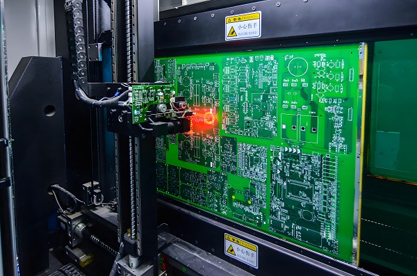
How is a TFT PCB Manufactured?
The production of TFT PCBs combines standard PCB processes with advanced assembly techniques:
1. Material Selection: FR4 is the most common for rigid PCBs, while polyimide is used for flexible TFT modules.
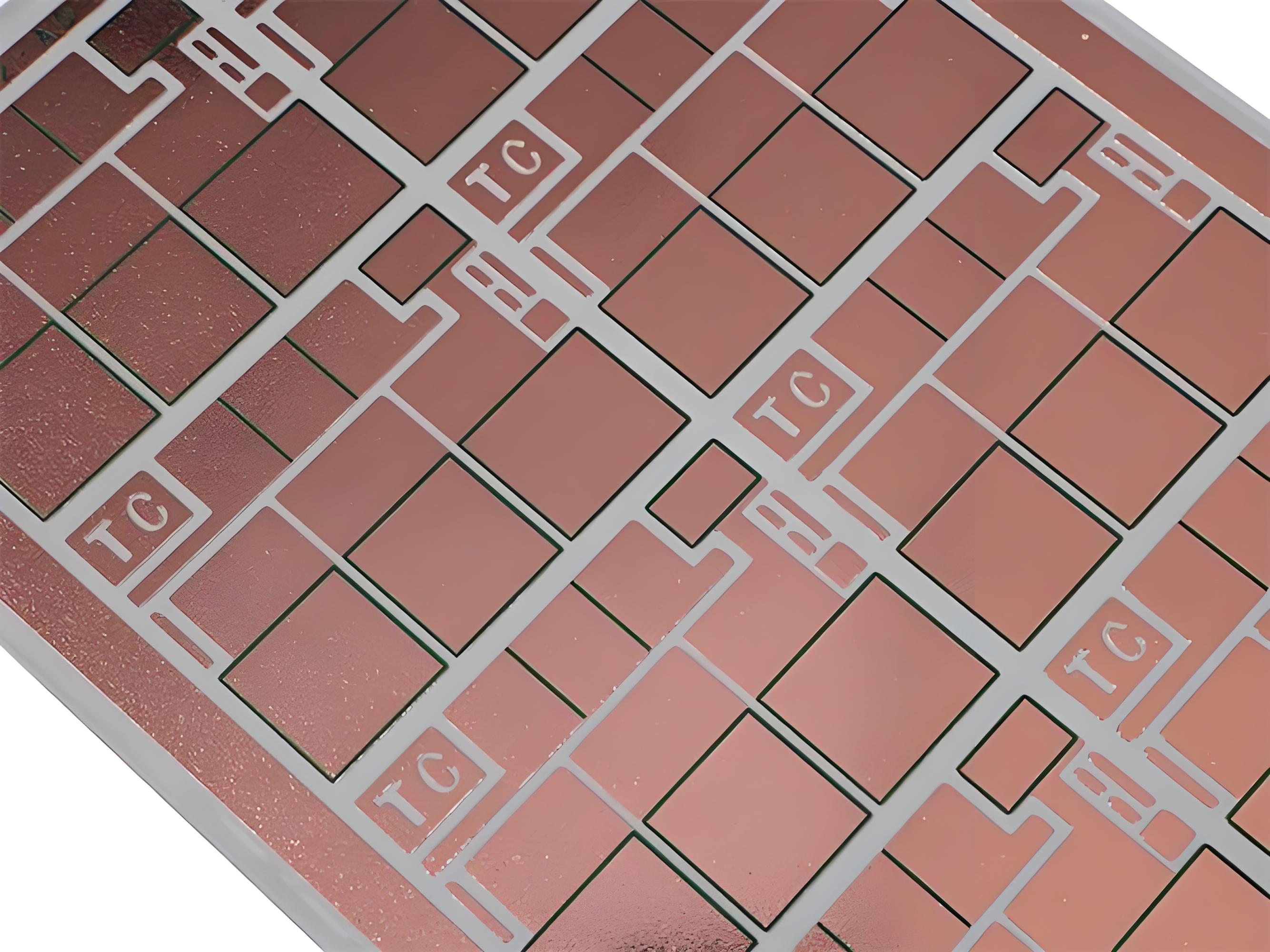
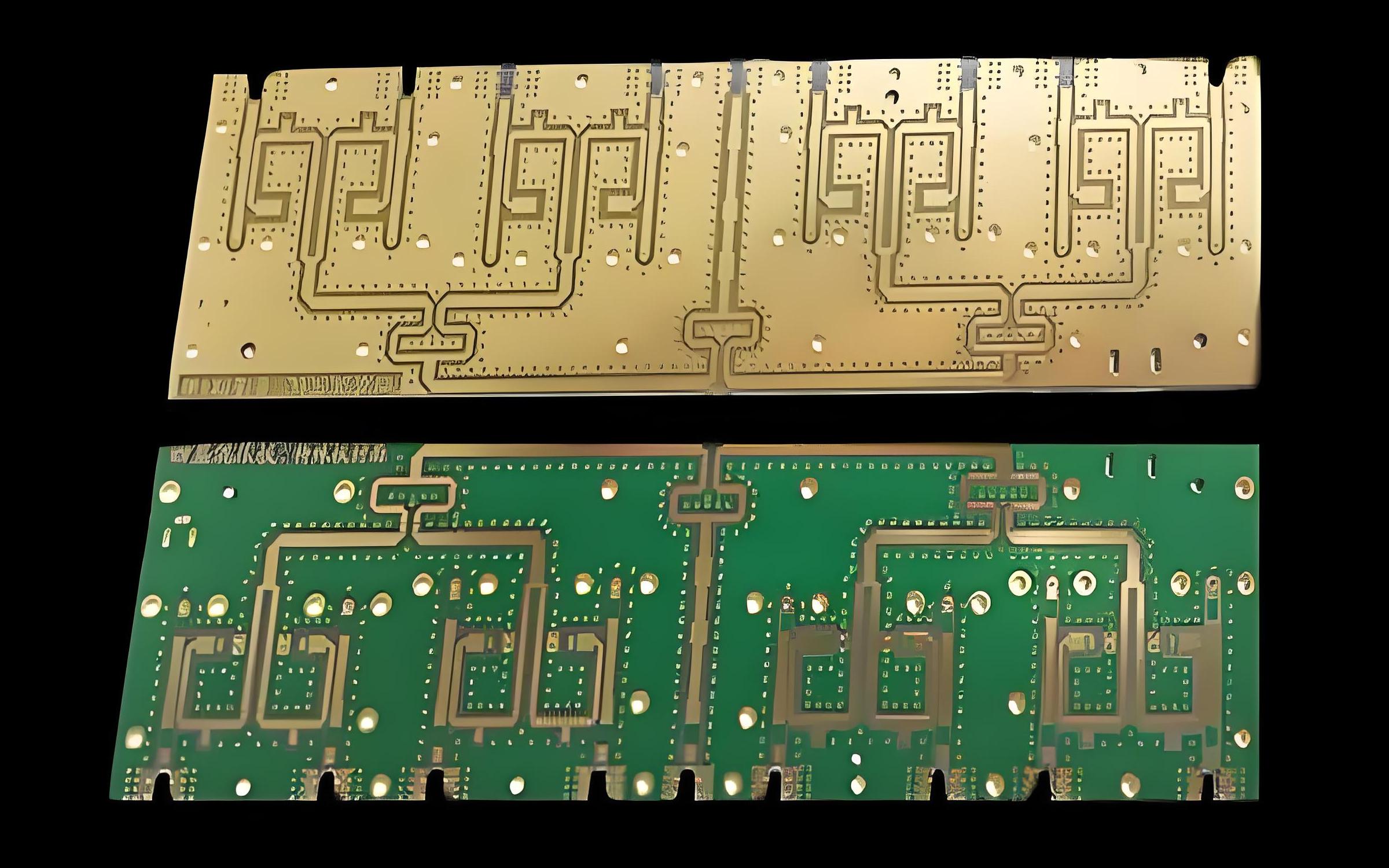
2. Copper Layering and Etching: Multiple copper layers are stacked and etched to create signal and power traces.
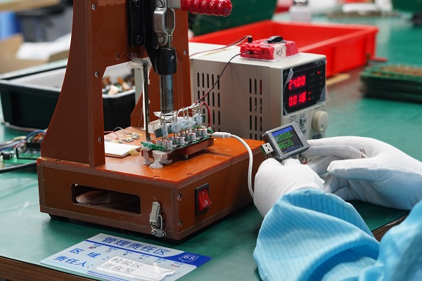
3. Surface Mount Assembly: Components like driver ICs and regulators are mounted using automated SMT machines.
4. Fine-Pitch Soldering: Since display connectors and ICs have extremely small pads, precision soldering is required.
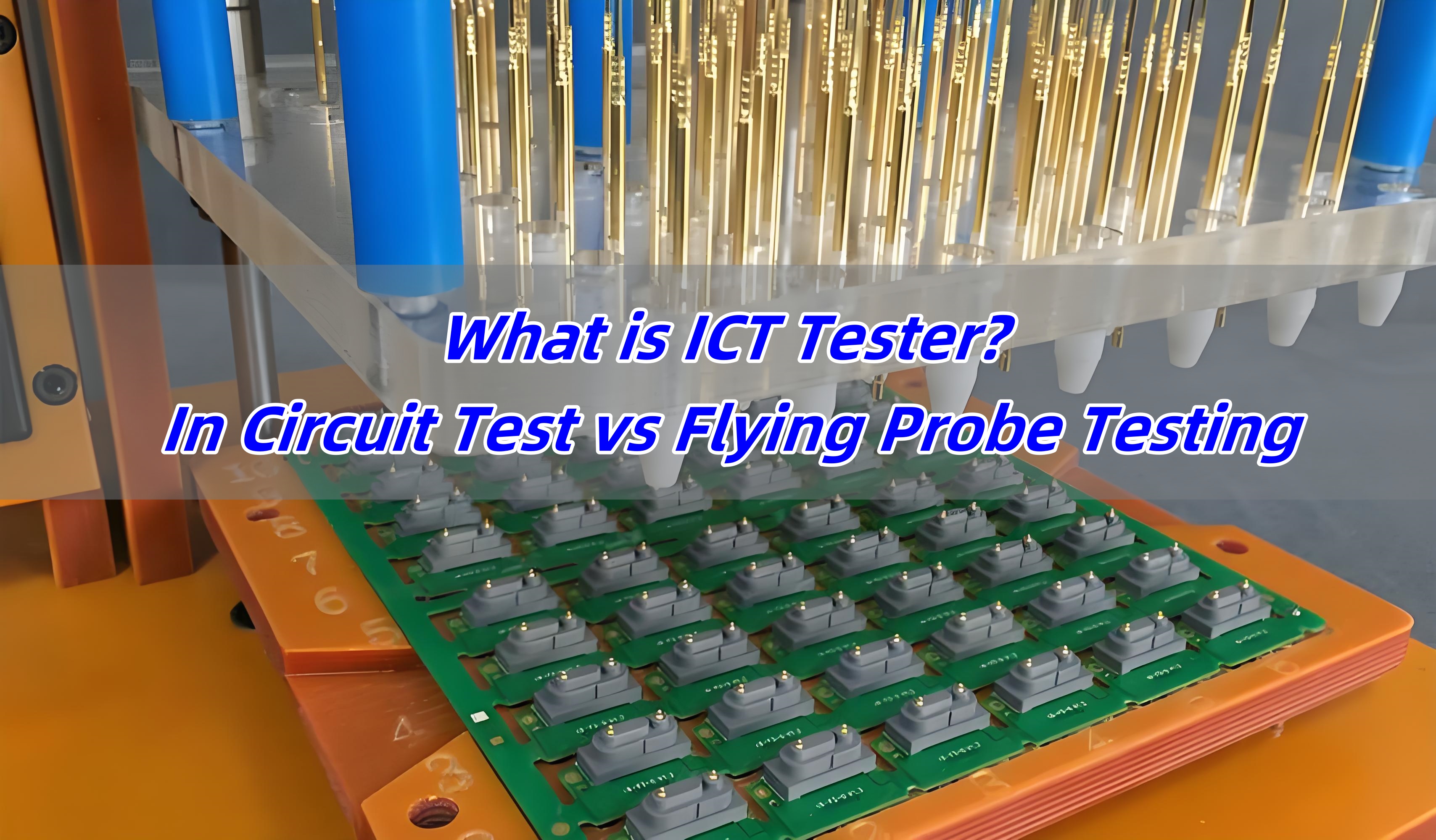
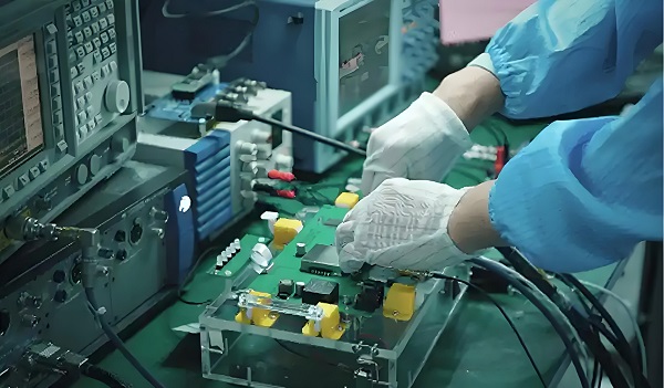
5. Testing: Includes electrical continuity, signal quality, and backlight performance checks.
6. Reliability Validation: For critical industries, additional tests such as thermal cycling, humidity resistance, and vibration are conducted.
The end result is a robust PCB that works seamlessly with the TFT glass, delivering both functionality and durability.
What is the Difference Between TFT PCB and Other Display PCBs?
Different display technologies require different PCB support.
- TFT PCB vs OLED PCB: OLEDs are self-illuminating, so their PCBs mainly manage signals and power, while TFT PCBs must also handle backlight circuits.
- TFT PCB vs LED Display PCB: LED display PCBs directly control thousands of LEDs in panels, often for outdoor or large-format use. TFT PCBs are designed for compact glass-based displays.
- Cost Comparison: TFT PCBs are usually less expensive than OLED PCBs, making them a cost-effective choice for many industries.
This is why TFT remains popular: it provides a balance between performance, cost, and maturity of technology.
Why Choose EBest Circuit (Best Technology) for TFT PCB Manufacturing?
As one of the best PCB manufacturers in China, our goal is to provide our customers with the best quality products and services at the most competitive pricing, and to become a reliable long-term partner of our customers in PCB manufacture and assembly.
Since its establishment in 2006 as a printed circuit board manufacturer, EBest Circuit (Best Technology) has focused on high-quality, low to medium-volume PCB fabrication, PCB assembly and electronics manufacturing. Our products and services include 1-100 layers printed circuit boards, thru-hole assembly, SMT assembly including BGA assembly, components sourcing, turnkey box build and electronic product development. From consumer electronics to advanced aerospace displays, EBest Circuit (Best Technology) has the capability and expertise to support projects of any scale.
FAQs
1. What materials are used in a TFT PCB?
Most TFT PCBs use FR4 for rigid sections and polyimide for flexible cables. Advanced materials may be used in high-frequency or high-reliability designs.
2. Can TFT PCBs support touch screen functions?
Yes. Capacitive or resistive touch controllers are often integrated into the PCB to handle user interactions.
3. How thin can a TFT PCB be?
Flexible TFT PCBs can be as thin as 0.15 mm, while rigid designs are typically 0.6–1.6 mm.
4. Are TFT PCBs different for automotive displays?
Yes. Automotive TFT PCBs are designed for durability, with heat-resistant materials, vibration tolerance, and wider operating temperature ranges.
5. What is the typical cost of a TFT PCB?
Costs vary based on size, layer count, and application. Consumer TFT PCBs are usually low-cost, while automotive and medical-grade boards cost more due to higher standards.