What Are PCB Letter Codes? — Definitions & Core Functions
PCB letter codes are essential identifiers used in printed circuit board (PCB) design and manufacturing, serving as a universal language to label components, layers, test points, and functional zones on a board. These PCB letter codes eliminate confusion during assembly, repair, and quality control, ensuring that engineers, technicians, and suppliers across the globe can quickly interpret a PCB’s layout and purpose. Whether you’re designing a new board, troubleshooting a faulty circuit, or sourcing replacement parts, understanding PCB letter codes is non-negotiable for streamlining processes and avoiding costly errors. Without clear, standardized letter codes, even simple tasks like identifying a resistor or navigating a multi-layer PCB would become time-consuming and error-prone.
International Standards & Design Specifications for PCB Letter Codes (IEEE/IPC Standards Explained)
When working with PCB letter codes, adherence to international standards is critical to ensure compatibility and clarity. The two most widely recognized standards are IEEE (Institute of Electrical and Electronics Engineers) and IPC (Association Connecting Electronics Industries), each outlining guidelines for consistent PCB letter codes usage. IEEE standards, such as IEEE 315, focus on component labeling conventions, while IPC standards like IPC-2221 detail general PCB design requirements, including letter code formatting for layers and test points. Following these standards ensures that your PCB letter codes are understandable to anyone working with the board, regardless of their location or industry. For example, IPC specifies that power-related components should use letter codes starting with “P” (e.g., P1 for Power Connector), while IEEE mandates that resistors use “R” (e.g., R12 for Resistor 12). Ignoring these standards can lead to miscommunication, delayed projects, and incompatible components.
pcb code list (Comprehensive Common PCB Letter Codes Reference Table)
Having a reliable reference for common PCB letter codes saves time and reduces guesswork. Below is a complete, industry-aligned list of PCB letter codes (per IEEE 315 and IPC-2221 standards), covering passive components, active components, connectors, power elements, test points, and specialized parts:
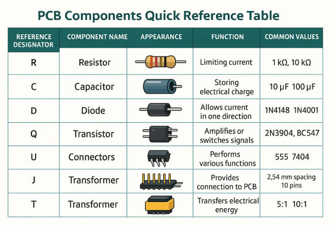
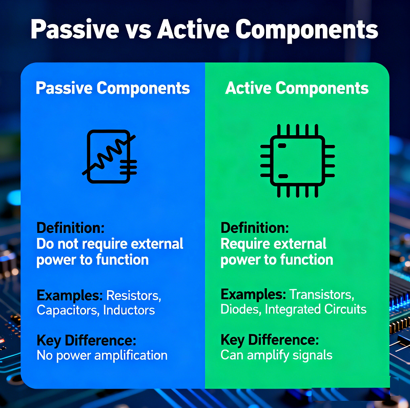
1. Passive Components (Basic Electrical Components)
- R: Resistor (e.g., R001 = Resistor 1; R105 = Resistor 105)
- RN: Network Resistor (e.g., RN08 = Resistor Network 8)
- RP: Power Resistor (e.g., RP22 = Power Resistor 22)
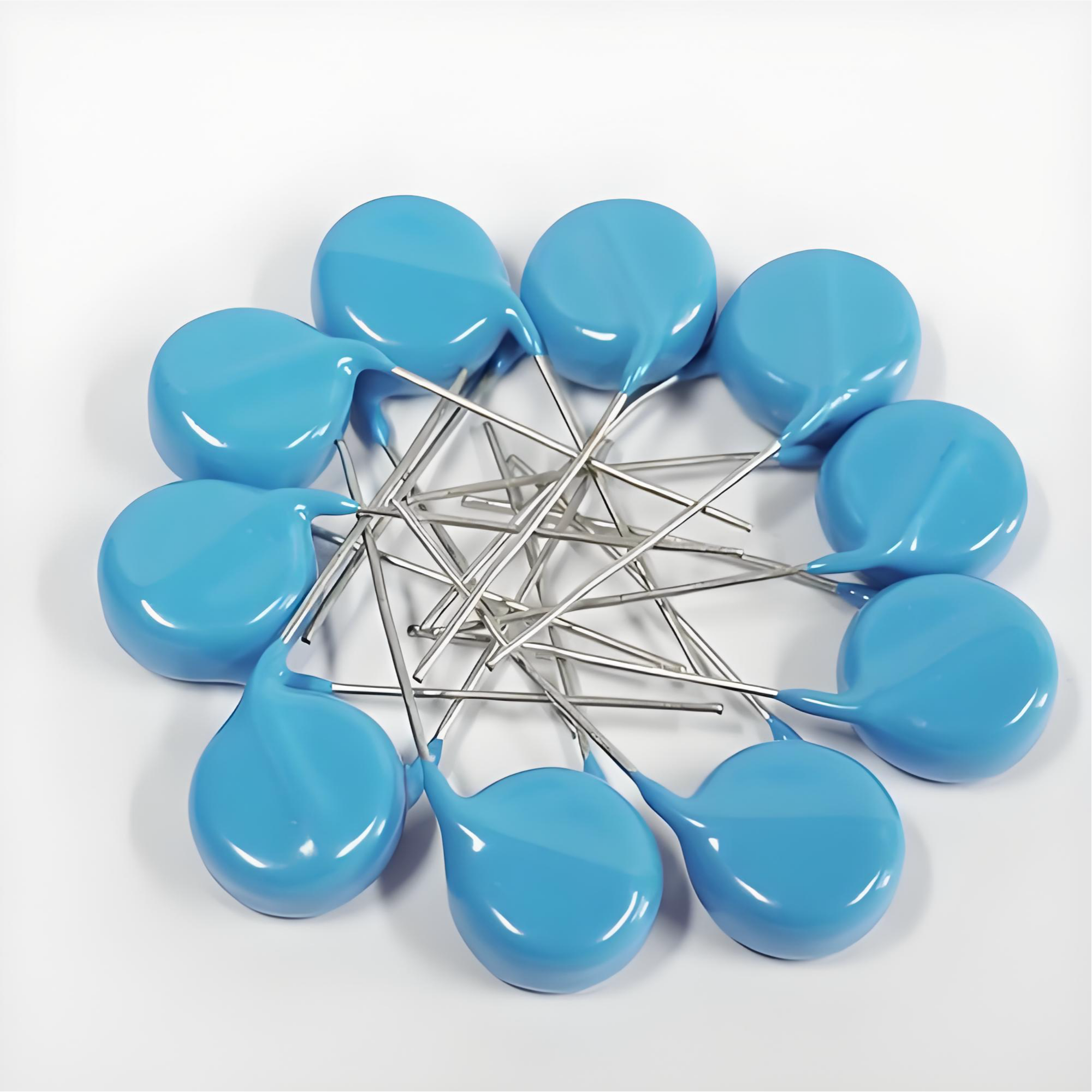
- C: Capacitor (e.g., C023 = Capacitor 23; C450 = Capacitor 450)
- CP: Power Capacitor (e.g., CP19 = Power Capacitor 19)
- CF: Film Capacitor (e.g., CF07 = Film Capacitor 7)
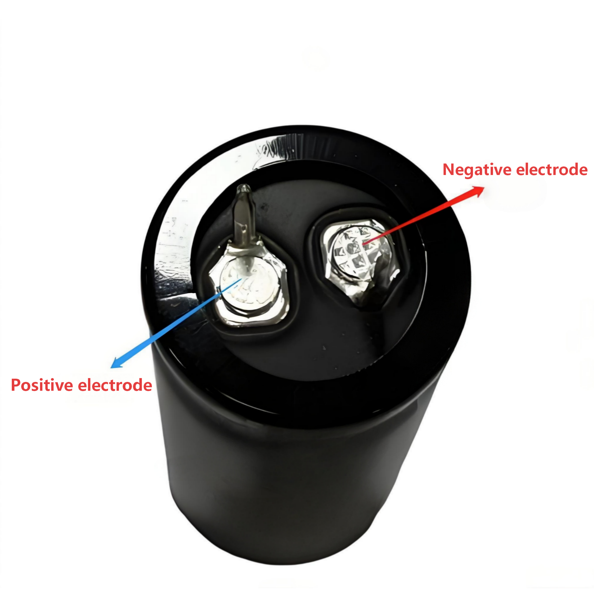
- CE: Electrolytic Capacitor (e.g., CE31 = Electrolytic Capacitor 31)
- CL: Ceramic Capacitor (e.g., CL14 = Ceramic Capacitor 14)
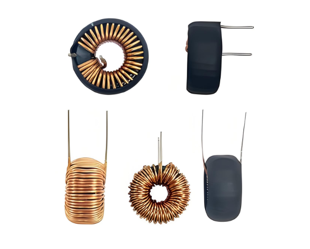
- L: Inductor (e.g., L009 = Inductor 9; L88 = Inductor 88)
- LF: Ferrite Inductor (e.g., LF56 = Ferrite Inductor 56)
- LT: Toroidal Inductor (e.g., LT04 = Toroidal Inductor 4)
- X: Crystal Oscillator (e.g., X12 = Crystal 12; X008 = Crystal 8)
- XTAL: High-Precision Crystal (e.g., XTAL03 = Precision Crystal 3)
- Z: Varistor (e.g., Z17 = Varistor 17; Z99 = Varistor 99)
- VR: Variable Resistor/Potentiometer (e.g., VR06 = Potentiometer 6)
- RV: Varicap (Variable Capacitor) (e.g., RV28 = Varicap 28)
- F: Fuse (e.g., F03 = Fuse 3; F111 = Fuse 111)
- FB: Fuse Block (e.g., FB05 = Fuse Block 5)
- FD: Diode Fuse (e.g., FD18 = Diode Fuse 18)
- TC: Thermistor (e.g., TC44 = Thermistor 44)
- RT: Temperature-Sensitive Resistor (e.g., RT77 = Temp Resistor 77)
2. Active Components (Semiconductors & Integrated Circuits)
- D: Diode (e.g., D008 = Diode 8; D300 = Diode 300)
- LED: Light-Emitting Diode (e.g., LED07 = LED 7; LED120 = LED 120)
- LD: Laser Diode (e.g., LD02 = Laser Diode 2)
- ZD: Zener Diode (e.g., ZD15 = Zener Diode 15)
- SD: Schottky Diode (e.g., SD41 = Schottky Diode 41)
- Q: Transistor (BJT) (e.g., Q11 = Transistor 11; Q89 = Transistor 89)
- MOS: MOSFET (e.g., MOS09 = MOSFET 9; MOS201 = MOSFET 201)
- JFET: Junction Field-Effect Transistor (e.g., JFET13 = JFET 13)
- IGBT: Insulated-Gate Bipolar Transistor (e.g., IGBT06 = IGBT 6)
- U: Integrated Circuit (IC) (e.g., U04 = IC 4; U55 = IC 55)
- MCU: Microcontroller Unit (e.g., MCU01 = Microcontroller 1)
- CPU: Central Processing Unit (e.g., CPU02 = CPU 2)
- RAM: Random Access Memory (e.g., RAM08 = RAM Module 8)
- ROM: Read-Only Memory (e.g., ROM14 = ROM Chip 14)
- OP: Operational Amplifier (e.g., OP33 = Op-Amp 33)
- REG: Voltage Regulator (e.g., REG29 = Voltage Regulator 29)
- ADC: Analog-to-Digital Converter (e.g., ADC17 = ADC 17)
- DAC: Digital-to-Analog Converter (e.g., DAC05 = DAC 5)
- IC: Generic Integrated Circuit (alternate to U) (e.g., IC78 = IC 78)
- SCR: Silicon Controlled Rectifier (e.g., SCR30 = SCR 30)
- TRIAC: Triode AC Switch (e.g., TRIAC04 = TRIAC 4)
3. Connectors & Interfaces
- J: General Connector (e.g., J02 = Connector 2; J100 = Connector 100)
- JP: Jumper (e.g., JP09 = Jumper 9; JP45 = Jumper 45)
- CON: Multi-Pin Connector (e.g., CON18 = Connector 18)
- USB: USB Port (e.g., USB01 = USB Port 1; USB03 = USB Port 3)
- HDMI: HDMI Port (e.g., HDMI02 = HDMI Port 2)
- ETH: Ethernet Port (e.g., ETH01 = Ethernet Port 1; ETH05 = Ethernet Port 5)
- VGA: VGA Port (e.g., VGA01 = VGA Port 1)
- AUX: Auxiliary Port (e.g., AUX07 = Aux Port 7)
- DC: DC Power Jack (e.g., DC04 = DC Jack 4)
- AC: AC Power Connector (e.g., AC02 = AC Connector 2)
- BT: Battery Terminal (e.g., BT08 = Battery Terminal 8)
- TP: Test Point (e.g., TP15 = Test Point 15; TP200 = Test Point 200)
- TPG: Ground Test Point (e.g., TPG03 = Ground Test Point 3)
- TPS: Signal Test Point (e.g., TPS19 = Signal Test Point 19)
4. Power & Energy Components
- P: Power Connector (e.g., P01 = Power Connector 1; P67 = Power Connector 67)
- PG: Power Ground (e.g., PG05 = Power Ground 5)
- PV: Power Voltage (e.g., PV3V3 = 3.3V Power Rail; PV5V = 5V Power Rail)
- B: Battery (e.g., B01 = Battery 1; B03 = Battery 3)
- CH: Charger (e.g., CH09 = Charger Module 9)
- PSU: Power Supply Unit (e.g., PSU02 = Power Supply 2)
- TR: Transformer (e.g., TR11 = Transformer 11; TR88 = Transformer 88)
- CT: Current Transformer (e.g., CT07 = Current Transformer 7)
- VT: Voltage Transformer (e.g., VT14 = Voltage Transformer 14)
5. Mechanical & Specialized Components
- M: Motor (e.g., M03 = Motor 3; M12 = Motor 12)
- HS: Heat Sink (e.g., HS06 = Heat Sink 6)
- FAN: Cooling Fan (e.g., FAN04 = Fan 4)
- S: Switch (e.g., S08 = Switch 8; S99 = Switch 99)
- SW: Toggle Switch (e.g., SW17 = Toggle Switch 17)
- PB: Push Button (e.g., PB22 = Push Button 22)
- REL: Relay (e.g., REL05 = Relay 5; REL31 = Relay 31)
- SOL: Solenoid (e.g., SOL09 = Solenoid 9)
- SS: Slide Switch (e.g., SS13 = Slide Switch 13)
- LS: Limit Switch (e.g., LS04 = Limit Switch 4)
- OPT: Optocoupler/Optoisolator (e.g., OPT18 = Optocoupler 18)
- SENSOR: Generic Sensor (e.g., SENSOR07 = Sensor 7)
- TEMP: Temperature Sensor (e.g., TEMP24 = Temp Sensor 24)
- PRESS: Pressure Sensor (e.g., PRESS11 = Pressure Sensor 11)
- LDR: Light-Dependent Resistor (e.g., LDR08 = LDR 8)
This comprehensive PCB letter codes list covers 95% of components used in consumer electronics, industrial equipment, automotive PCBs, medical devices, and aerospace applications. For ultra-specialized use cases (e.g., military-grade PCBs), additional industry-specific codes may apply, but this table serves as the definitive reference for standard PCB design and manufacturing workflows.
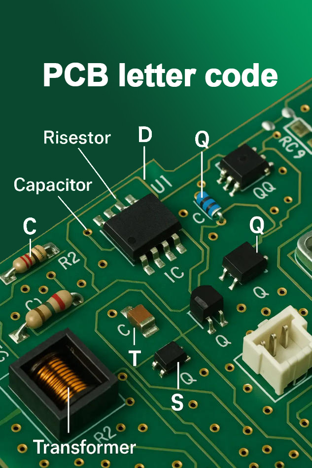
pcb components identification (PCB Component Identification: Quick Mapping from Codes to Physical Parts)
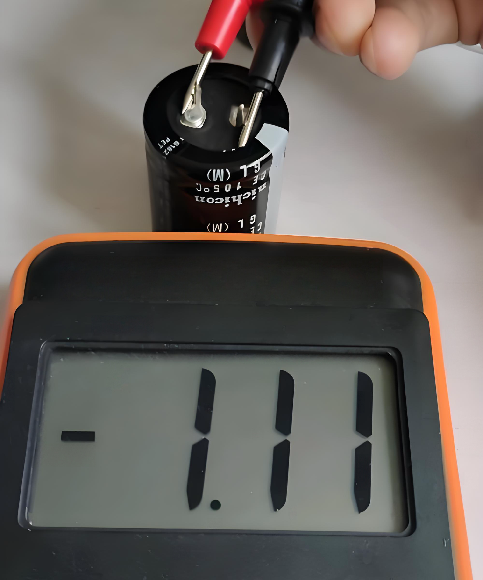
Translating PCB letter codes to physical components requires a combination of visual inspection and basic knowledge of component types. Start by locating the printed letter code on the PCB—this is typically printed near the component itself. Next, cross-reference the code with the list above to identify the component category (e.g., “C” for capacitor). Then, use physical characteristics to confirm: resistors are often cylindrical or rectangular with color bands, capacitors are small and cylindrical or rectangular, and ICs are larger with multiple pins. For example, if you see “U06” on the board, you’ll know to look for a multi-pin integrated circuit nearby. This PCB components identification process becomes faster with practice, but having a cheat sheet of PCB letter codes and component shapes will accelerate your workflow. For hard-to-identify components, use a digital multimeter to test functionality, which can confirm if a component matches its labeled code.
Numbering Rules for PCB Letter Codes (Sequential Numbering, Zonal Numbering, Multi-layer Board Numbering)
PCB letter codes aren’t just random labels—they follow specific numbering rules to ensure organization and scalability. The three most common numbering systems are:
- Sequential Numbering: This is the simplest method, where components are numbered in the order they’re placed on the PCB (e.g., R01, R02, R03…). It’s ideal for small, simple PCBs with few components.
- Zonal Numbering: For larger PCBs, components are grouped by zone (e.g., top-left, power section) and numbered within each zone (e.g., R101 for Resistor in Zone 1, Position 1; R205 for Resistor in Zone 2, Position 5). This makes it easier to locate components in complex layouts.
- Multi-layer Board Numbering: Multi-layer PCBs add a layer identifier to the code (e.g., R3-09 for Resistor on Layer 3, Position 9). This is critical for distinguishing components on different layers, which is essential during assembly and repair.
Understanding these PCB letter codes numbering rules helps you navigate any PCB design, whether it’s a small hobby board or a large industrial PCB. Consistency in numbering also ensures that your PCB letter codes are compatible with CAD software and manufacturing processes.
Detailed Explanation of Special-Function PCB Letter Codes (Power Supply, Test Points, Interface Codes)
Beyond standard component labels, PCB letter codes include special-function codes for critical board features. These codes are designed to highlight important areas and simplify maintenance:
- Power Supply Codes: These start with “P” (e.g., P3V3 for 3.3V Power Rail, P5V for 5V Power Rail) and indicate voltage levels or power distribution points. They’re vital for avoiding short circuits and ensuring proper power delivery.
- Test Point Codes: Labeled with “TP” (e.g., TP_VIN for Input Voltage Test Point, TP_GND for Ground Test Point), these codes mark points where technicians can measure signals or voltages during testing. They eliminate the need to probe sensitive components directly.
- Interface Codes: These identify external connections, such as “USB1” for USB Port 1, “ETH0” for Ethernet Port 0, or “HDMI2” for HDMI Port 2. They make it easy to map external devices to the PCB’s internal circuitry.
Mastering these special-function PCB letter codes is key for anyone involved in PCB testing, repair, or system integration. They reduce the risk of mistakes and make complex boards more manageable.
Recommended Practical Tools & Resources for Decoding PCB Letter Codes
Decoding PCB letter codes becomes even easier with the right tools and resources. Here are our top recommendations for both beginners and professionals:
- Digital Multimeters: A basic multimeter can test components (e.g., resistors, capacitors) to confirm their identity, complementing the letter code label.
- PCB CAD Software: Tools like Altium Designer, KiCad, or Eagle include built-in PCB letter codes libraries and validation features to ensure compliance with standards.
- Online Databases: Websites like IPC’s standards library or IEEE Xplore provide access to official PCB letter codes specifications for advanced users.
- Mobile Apps: Apps like “PCB Component Identifier” or “Electronics Reference” offer on-the-go access to PCB letter codes lists and component identification guides.
These tools streamline the process of working with PCB letter codes, whether you’re in the office, workshop, or field. Investing in reliable resources will save you time and improve the accuracy of your work.
3 Core Tips for Beginners to Master PCB Letter Codes Quickly
If you’re new to PCB letter codes, these three tips will help you master them in no time:
- Memorize High-Frequency Codes: Start by learning the most common codes (R, C, D, U, J) since they appear on nearly every PCB. Write them down or use flashcards for quick recall.
- Practice with Real PCBs: Grab old electronics (e.g., smartphones, routers) and identify components using their PCB letter codes. This hands-on practice is far more effective than just reading lists.
- Stick to Standards: Always reference IEEE or IPC standards when working with PCB letter codes. Avoid creating custom codes unless absolutely necessary, as this can cause confusion for others.
By focusing on these fundamentals, you’ll build confidence and proficiency with PCB letter codes in weeks, not months.
Application Cases of PCB Letter Codes in Different Scenarios (Repair, Design, Procurement)
PCB letter codes are versatile and used across multiple stages of the PCB lifecycle. Here are real-world examples of how they’re applied:
- Repair: A technician troubleshooting a faulty TV PCB sees the code “Q04” near a burnt component. Using the PCB letter codes list, they identify it as a transistor, source a replacement, and fix the issue in minutes.
- Design: An engineer designing a medical device PCB uses zonal numbering for PCB letter codes (e.g., R302 for Resistor in the Sensor Zone). This helps the assembly team quickly locate components and ensures compliance with regulatory standards.
- Procurement: A buyer sourcing components for a production run references the PCB letter codes on the bill of materials (BOM) to order the correct resistors (R01-R50) and capacitors (C01-C35). This eliminates ordering errors and delays.
In each scenario, PCB letter codes improve efficiency, reduce mistakes, and ensure clear communication between teams.
Common Misunderstandings & Pitfalls of PCB Letter Codes
Even experienced professionals can fall prey to misunderstandings when working with PCB letter codes. Here are the most common pitfalls to avoid:
- Ignoring Standard Differences: Assuming IEEE and IPC PCB letter codes are identical is a mistake. For example, some IPC codes for test points differ from IEEE, so always confirm which standard the PCB uses.
- Custom Code Overload: Creating too many custom PCB letter codes for specialized components can make the board unreadable to others. Use custom codes sparingly and document them clearly.
- Poor Placement: Printing PCB letter codes too close to components or in hard-to-see areas (e.g., under large ICs) makes them useless. Ensure codes are visible and easily accessible.
- Inconsistent Numbering: Mixing sequential and zonal numbering on the same PCB causes confusion. Stick to one system throughout the design.
By avoiding these pitfalls, you’ll ensure that your PCB letter codes are effective and user-friendly.
FAQ: Frequently Asked Questions About PCB Letter Codes
Q1: Do different manufacturers use different PCB letter codes?
A1: While most manufacturers follow IEEE or IPC standards for PCB letter codes, some may use custom variations for specialized products. Always check the PCB’s datasheet or consult the manufacturer if you encounter unfamiliar codes.
Q2: What’s the difference between PCB letter codes for single-layer and multi-layer boards?
A2: Multi-layer boards add a layer identifier to PCB letter codes (e.g., R2-07 for Layer 2, Resistor 7), while single-layer boards use simple sequential or zonal numbering. This layer distinction is critical for assembly and repair.
Q3: I can’t find a matching component for a PCB letter code—what should I do?
A3: First, confirm the standard (IEEE/IPC) used for the PCB letter codes. If the code is still unrecognizable, check the PCB’s BOM or contact the original equipment manufacturer (OEM) for clarification. You can also use a component tester to identify the part’s function.
Q4: Can I create my own PCB letter codes for a custom project?
A4: You can, but it’s not recommended unless the project is for personal use. Custom PCB letter codes can cause confusion for anyone else working on the board. If you must use custom codes, document them clearly and share the reference with your team.
Q5: Are PCB letter codes required for small hobby PCBs?
A5: They’re not mandatory, but using PCB letter codes on hobby PCBs is a good practice. It makes assembly easier, helps with troubleshooting, and prepares you for professional projects where codes are standard.
Q6: How do I handle conflicting PCB letter codes on a board?
A6: Conflicting codes (e.g., two components labeled “R05”) usually indicate a design error. Cross-reference the PCB with the BOM to confirm the correct labels, and contact the designer or manufacturer to resolve the issue before proceeding with assembly or repair.
Conclusion: Efficient Application Methodology for PCB Letter Codes
PCB letter codes are the backbone of clear communication in PCB design, manufacturing, and maintenance. By understanding their definitions, following international standards, using practical tools, and learning from real-world applications, you can leverage PCB letter codes to streamline your workflow, reduce errors, and improve collaboration. Whether you’re a beginner or a seasoned professional, mastering these codes is essential for success in the electronics industry.
If you’re in need of high-quality PCBs with accurate, standardized PCB letter codes that meet IEEE and IPC standards, look no further. We specialize in manufacturing custom PCBs tailored to your specific needs, with clear PCB letter codes that simplify assembly, repair, and compliance. Don’t let confusing or inconsistent codes slow down your project—place your order today by emailing us at sales@bestpcbs.com. Our team is ready to deliver reliable, industry-compliant PCBs that meet your deadlines and exceed your expectations.