Why choose MCPCB for LED applications? This guide explores metal core PCB specifications, material comparisons (copper vs aluminum), advanced heat dissipation techniques, and practical design solutions for optimal LED performance.
- “Insufficient heat dissipation of high-power LEDs leads to accelerated light decay and substandard product lifespan?”
- “The processing cost of aluminum substrates is low, but the unstable welding yield affects mass production efficiency?”
- “The traditional MCPCB is heavy, which limits the design of lightweight lamps?”
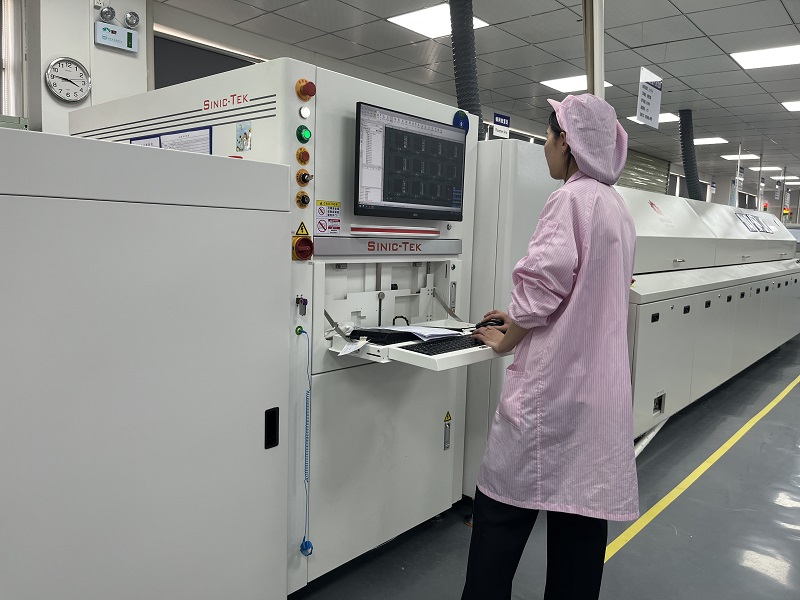
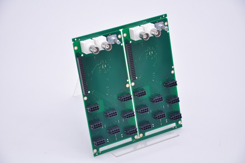
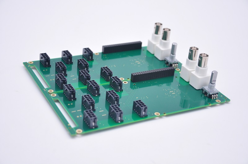
EBest Circuit (Best Technology) Can Provide
- The copper-based MCPCB (thermal conductivity of more than 380W/mK) is used with a high thermal conductivity insulation layer to ensure that the core temperature is 15-20℃ lower than that of the aluminum substrate, extending the LED life by more than 30%.
- Patented surface treatment technology (such as enhanced OSP+ laser etching) achieves zero oxidation of the pad, and the SMT yield is increased to 99.2%, which is compatible with the full process of reflow soldering/wave soldering.
- Ultra-thin aluminum substrate (0.8mm thickness) + hollow structure design reduces weight by 40% while maintaining heat dissipation performance, and has been successfully applied to compact scenes such as downlights or car lights.
Welcome to contact us if you have any request for MCPCB: sales@bestpcbs.com.
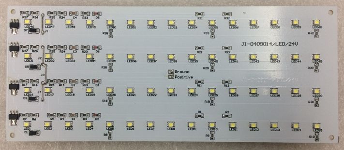
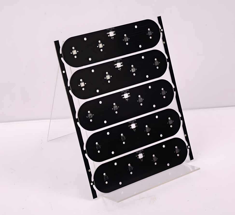
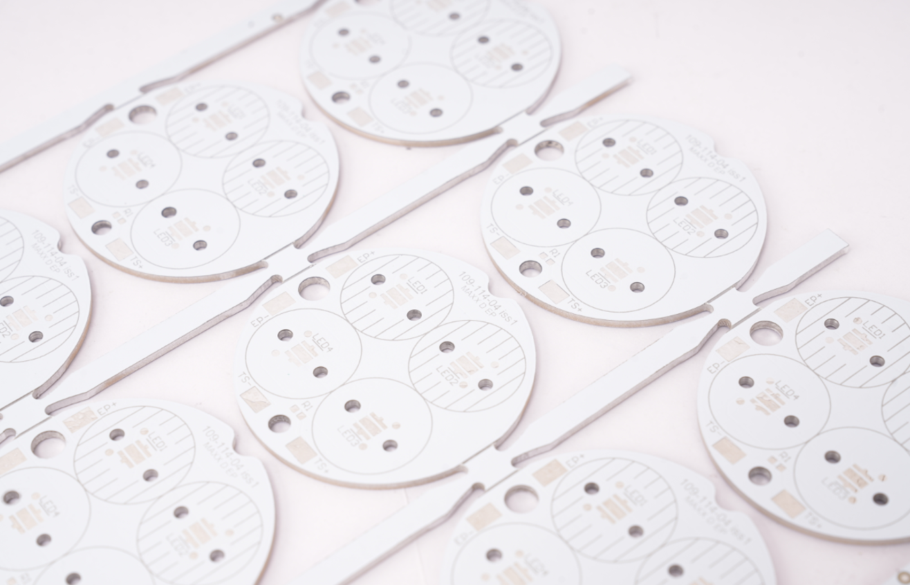
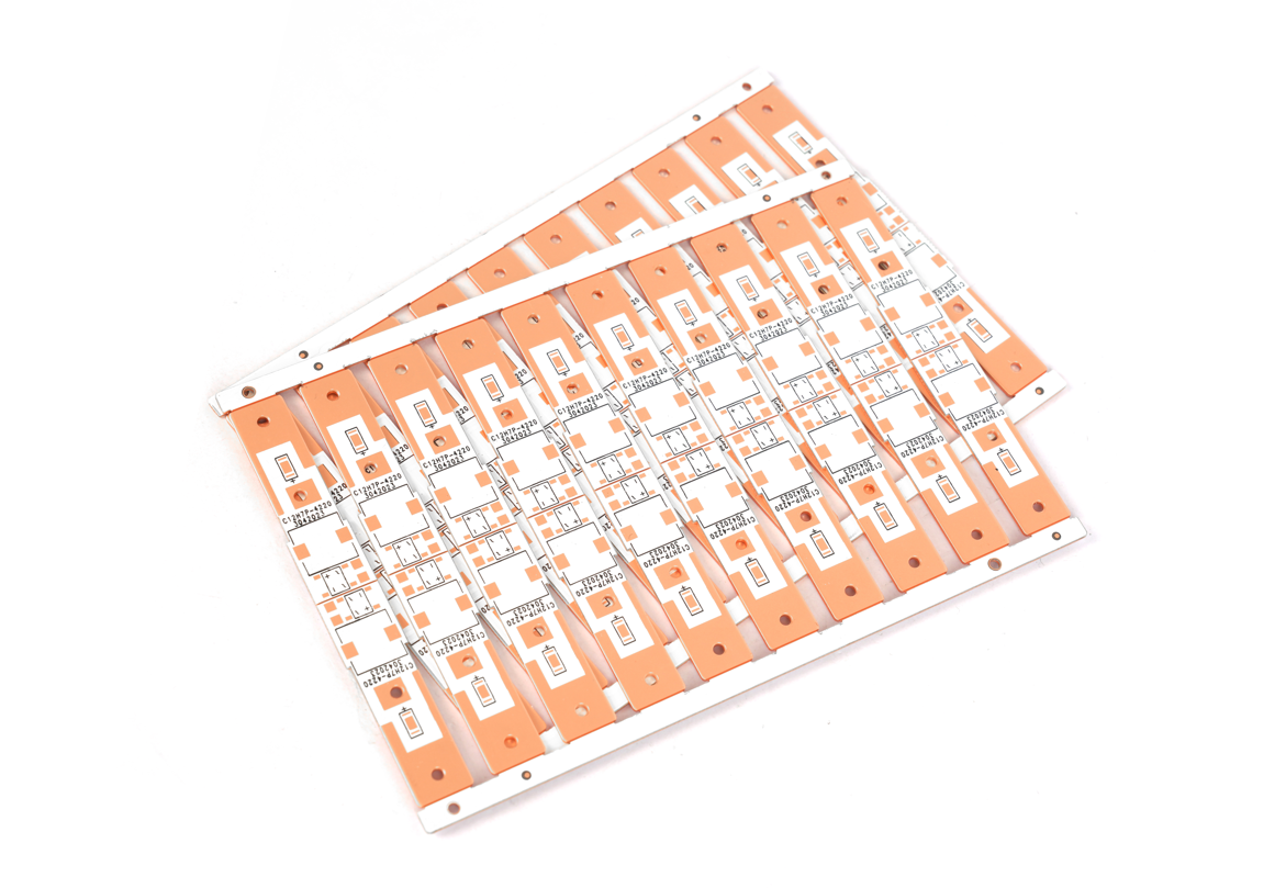
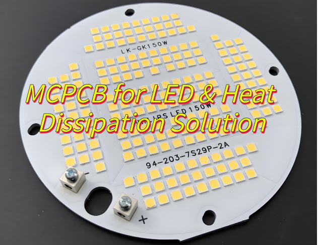
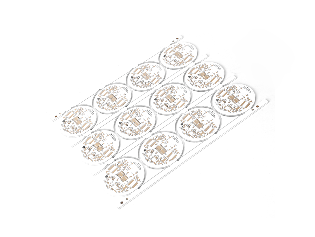
What Is MCPCB for LED?
A MCPCB for LED is a specialized thermal management solution that efficiently dissipates heat from high-power LED components. The board features a layered construction with a metal base (typically aluminum), a thermally conductive dielectric layer, and copper circuitry.
This design allows rapid heat transfer away from LED chips, maintaining optimal operating temperatures and preventing premature failure. The metal core’s high thermal conductivity (5-10 times better than standard PCBs) ensures stable light output and color consistency in demanding applications like automotive lighting, street lamps, and architectural illumination.
By reducing thermal resistance between LEDs and heatsinks, MCPCBs extend product lifespan while enabling more compact, high-density LED array designs. Their structural integrity also minimizes thermal expansion issues during temperature fluctuations.
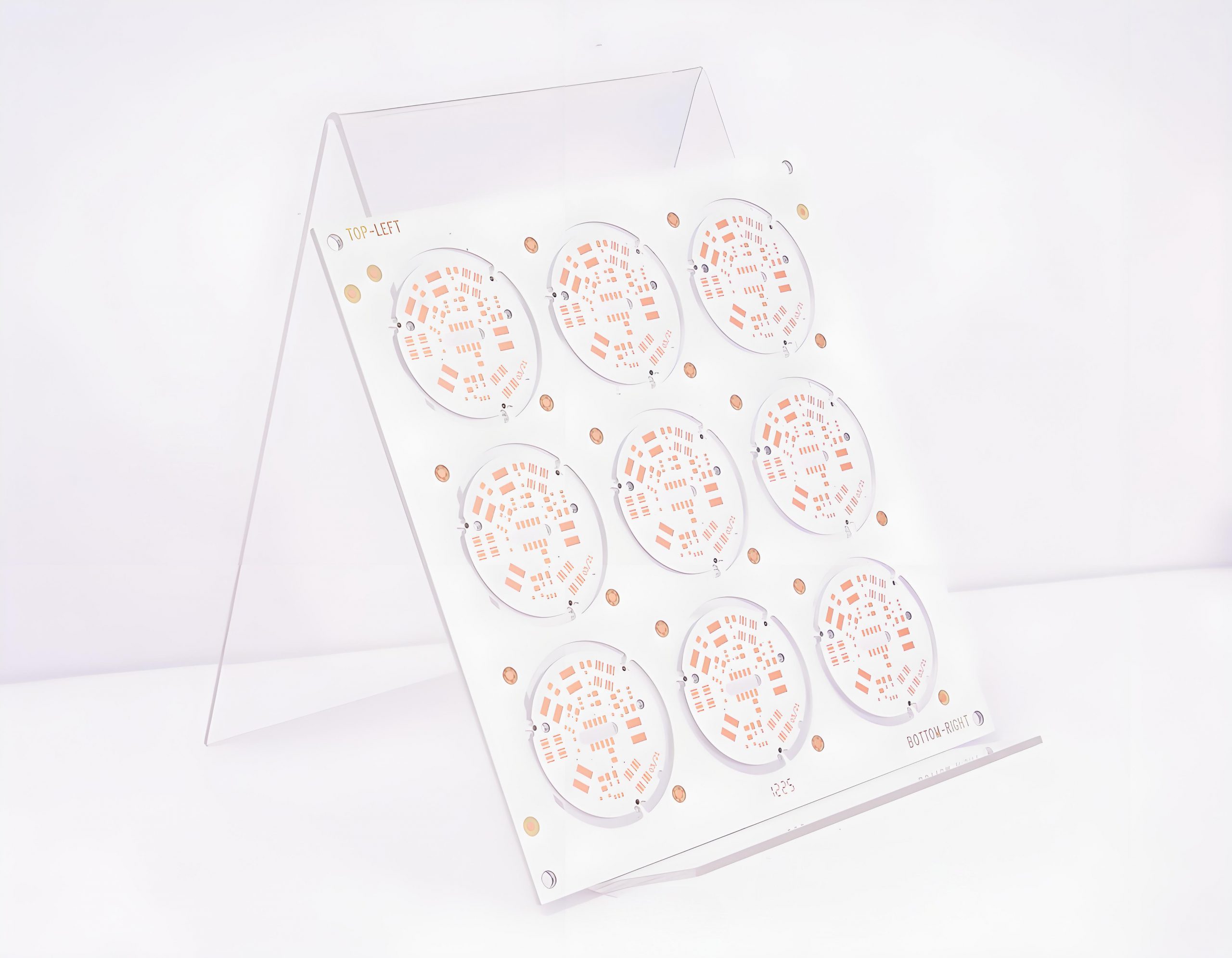
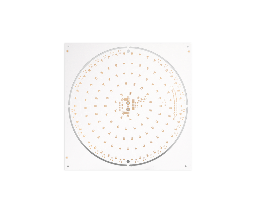
MCPCB for LED Specification
Here are the technical specifications for MCPCBs used in LED applications:
Base Material Properties
- Thickness: 0.8mm to 3.0mm
- Thermal conductivity: 1-400 W/mK
- Aluminum alloys: 5052, 6061 (typical)
- Copper purity: ≥99.9% for copper cores
Dielectric Layer Characteristics
- Thickness: 50-150μm
- Dielectric strength: 2-6kV
- Thermal resistance: 0.3-1.5°C-in²/W
Copper Circuit Specifications
- Foil thickness: 1oz (35μm) to 4oz (140μm)
- Minimum line width: 0.1mm
- Minimum spacing: 0.1mm
- Surface finishes: HASL, ENIG, OSP
Thermal Performance Metrics
- Junction-to-board thermal resistance: 0.5-3.0°C/W
- Maximum operating temperature: 130-150°C
- Coefficient of thermal expansion: 20-24 ppm/°C
Mechanical Specifications
- Bend strength: 25-40N/mm²
- Flatness tolerance: ≤0.15mm/100mm
- Hole size capability: 0.3mm minimum
Electrical Properties
- Breakdown voltage: ≥2kV
- Insulation resistance: ≥10⁸Ω
- Dielectric constant: 3.5-5.0 @1MHz
LED-Specific Parameters
- SMD pad dimensions: matching standard packages
- Solder mask reflectance: 85-92% (white)
- Thermal pad coverage: ≥80% of LED footprint
Environmental Compliance
- Operating temperature range: -40°C to +150°C
- Storage temperature range: -55°C to +155°C
- Relative humidity: 5-95% non-condensing
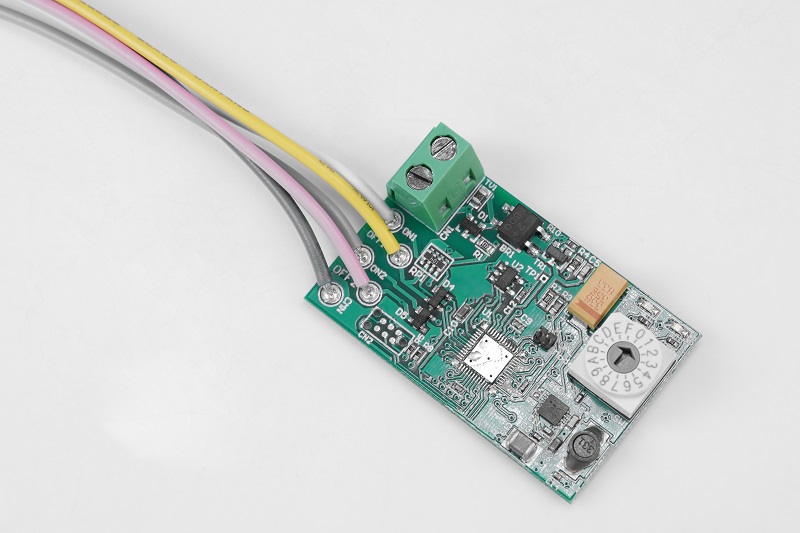
What Is Use of MCPCB for LED Light?
Here are the primary uses of MCPCB for LED lighting:
- Heat dissipation – Transfers heat 8x faster than standard FR4 PCBs to prevent LED performance degradation.
- Thermal management – Handles 2-5W high-power LEDs by preventing heat accumulation.
- Lifespan extension – Maintains lower operating temperatures to prolong LED service life.
- Structural stability – Provides dimensional consistency across temperature fluctuations.
- Electrical insulation – Dielectric layers enable safe current flow while conducting heat.
- Space optimization – Integrated metal core replaces separate heat sinks in compact designs.
- Light consistency – Maintains optimal junction temperatures for stable luminous output.

Copper MCPCB vs Aluminum MCPCB for LED Light
Here’s a structured comparison between copper and aluminum MCPCBs for LED lighting applications:
Thermal Performance
- Copper: Superior thermal conductivity (~380–400 W/mK), ideal for high-power LEDs or dense arrays where heat buildup is a concern.
- Aluminum: Moderate thermal conductivity (~150–200 W/mK), suitable for medium-power applications with adequate airflow.
Cost Efficiency
- Copper: 30–50% more expensive due to material costs and machining complexity.
- Aluminum: Budget-friendly with acceptable performance for most commercial LED products.
Weight and Mechanical Properties
- Copper: Heavier (3× aluminum), which may limit use in weight-sensitive applications (e.g., automotive, portable devices).
- Aluminum: Lightweight and easier to machine, enabling faster production and simpler handling.
Thermal Expansion Compatibility
- Copper: Closer CTE (17 ppm/°C) to LED chips (6–8 ppm/°C), reducing solder joint stress during thermal cycling.
- Aluminum: Higher CTE (23 ppm/°C) may require careful design to avoid long-term reliability issues.
Corrosion and Durability
- Copper: Prone to oxidation without surface treatments (e.g., ENIG, HASL).
- Aluminum: Naturally corrosion-resistant due to oxide layer formation.
Electrical Conductivity
- Copper: Better current distribution for complex circuits or high-current designs.
- Aluminum: Requires thicker traces to match copper’s conductivity but sufficient for standard LED layouts.
Manufacturing and Design Flexibility
- Copper: Demands specialized equipment for drilling/routing, increasing lead time and cost.
- Aluminum: Easier to process, supporting rapid prototyping and cost-effective mass production.
MCPCB Heat Dissipation Solution in High-Power LED Light
Here are practical high-efficiency thermal solutions for MCPCB in high-power LED applications:
- Multi-Layer Copper Cladding: Deploying 2-4oz copper foil layers (70-280μm) with optimized trace patterns to enhance lateral heat spreading across the board surface.
- Ceramic-Enhanced Dielectric: Using aluminum nitride (AlN) or boron nitride filled dielectric layers (5-20W/mK) to improve vertical heat transfer from LEDs to metal core.
- Micro-Channel Embedded Cooling: Integrating sub-millimeter fluid channels within aluminum cores for active liquid cooling in extreme power density applications.
- Thermal Via Arrays: Implementing high-density copper-plated through-holes (0.3-1mm diameter) beneath LED pads to create direct thermal pathways.
- Phase Change Materials: Incorporating paraffin-based PCM layers (melting point 50-80°C) to absorb and redistribute transient thermal loads.
- Graphene-Coated Interfaces: Applying few-layer graphene coatings (500-1500W/mK) at critical junctions to reduce interfacial thermal resistance.
- Topological Optimization: Applying generative design algorithms to create organic-shaped aluminum cores that maximize surface-area-to-volume ratio.
How to Design MCPCB Layout and Routing for Optimal Performance?
Here are practical MCPCB layout and routing strategies for optimal thermal and electrical performance in high-power LED applications:
- Thermal-Centric Component Placement: Position high-power LED components directly above the thickest metal core sections, maintaining minimum 3mm clearance from board edges to prevent thermal boundary effects.
- Symmetrical Power Distribution: Implement star-topology routing for power traces with equal-length branches to ensure uniform current distribution across parallel LED strings.
- Copper Thickness Optimization: Use 2-4oz copper layers for current-carrying traces, with wider traces (minimum 2mm width per 1A) to reduce resistive heating and improve heat spreading.
- Thermal Relief Patterns: Design circular thermal relief cutouts (0.5-1mm radius) around mounting holes to prevent heat accumulation while maintaining mechanical stability.
- Dielectric Layer Configuration: Select dielectric materials (3-8W/mK thermal conductivity) with thicknesses (75-150μm) that balance electrical isolation and thermal transfer requirements.
- Dynamic Current Balancing: Incorporate current mirror circuits with thermal-compensated resistors near LED clusters to maintain stable operation across temperature variations.
Examples of Metal Core PCB Heat Dissipation Solutions
Five Common Metal Core PCB (MCPCB) Heat Dissipation Solutions with Verified Data
1. High-Power LED Street Lighting
- Application: Municipal outdoor lighting systems using 100W+ LED modules.
- Challenge: Prolonged operation at elevated temperatures caused lumen degradation and shortened lifespan.
- Solution: Copper-based MCPCBs with embedded thermal vias and a 2mm thick core. The copper substrate directly bonded to the LED array, while aluminum heat sinks attached to the PCB backside enhanced convective cooling.
- Result: Junction temperature reduced by 40% (from 110°C to 66°C), extending operational life to 50,000+ hours (verified via accelerated aging tests).
2. Automotive Headlamp Assemblies
- Application: LED headlights in compact vehicles requiring minimal space.
- Challenge: High thermal density in confined enclosures led to thermal runaway risks.
- Solution: Aluminum MCPCBs with a 1.6mm thickness, featuring a serpentine copper trace layout to distribute heat evenly. A graphite thermal pad bridged the PCB and housing, leveraging the vehicle’s airflow for passive cooling.
- Result: Stable LED performance at 85°C ambient, with no measurable color shift (Δu’v’ < 0.005) over 10,000 hours (confirmed by spectrophotometer analysis).
3. Industrial UV Curing Systems
- Application: UV LED arrays used in printing and coating processes.
- Challenge: Intense UV radiation generated excessive heat, damaging adhesive bonds.
- Solution: Copper MCPCBs with a 3.2mm core and diamond-coated solder masks for durability. A phase-change thermal interface material (TIM) ensured optimal contact with liquid-cooled cold plates.
- Result: Thermal resistance lowered to 0.5°C/W (from 1.2°C/W in baseline designs), enabling continuous operation at 95% power without degradation (validated via thermal imaging and bond strength tests).
4. Industrial UV Curing Systems
- Application: Multi-spectrum LED panels for indoor farming.
- Challenge: Dense chip placement caused localized hotspots, affecting plant growth cycles.
- Solution: Aluminum MCPCBs with a staggered via pattern and copper-filled thermal zones. The boards integrated with passive aluminum fins and active fans for hybrid cooling.
- Result: Uniform temperature distribution across the panel (±3°C variance), with a 30% increase in photosynthetic photon flux density (PPFD) efficiency (measured via quantum sensor arrays).
5. Consumer Electronics Flash Modules
- Application: High-intensity LED flashes in smartphones and cameras.
- Challenge: Rapid heat buildup during short bursts caused user discomfort and component stress.
- Solution: Ultra-thin (0.8mm) copper MCPCBs with vapor chamber integration. The vapor chamber spread heat laterally, while ceramic-filled silicone gaskets insulated adjacent components.
- Result: Peak temperature during flash activation reduced by 25°C (from 85°C to 60°C), enabling 50% faster repeat firing without thermal throttling (confirmed via infrared thermography and cycle testing).
Instant Quote
This guide covers MCPCB essentials for LED from material selection (copper vs. aluminum) to thermal design and layout optimization. Whether you need high-power heat dissipation or cost-effective solutions, proper MCPCB engineering ensures LED longevity and performance. For precise cost estimation and technical solutions tailored to your LED project requirements, contact EBest Circuit (Best Technology) for professional consultation and quotation service: sales@bestpcbs.com.