The SMT PCBA process is the backbone of modern electronics manufacturing, involving the automated placement and soldering of components onto printed circuit boards. This article provides a comprehensive guide to building a stable SMT production line, with a special focus on the critical engineering controls needed for turnkey medical device projects.
Launching a medical device often stalls not at design, but at manufacturing—where compliance, reliability, and execution risks quickly compound.
- Lack of true medical compliance expertise beyond basic PCB assembly (ISO 13485, FDA QSR).
- Unstable sourcing for long-lifecycle medical components and obsolescence risk.
- Yield loss and inconsistency when assembling fine-pitch and miniature components.
- Heavy documentation and validation burdens for regulatory submissions.
- Fragmented communication in turnkey projects without clear ownership.
These challenges are addressed by partnering with a medical-focused EMS provider built around process control, traceability, and regulatory readiness.
- ISO 13485–certified quality system with audit-ready workflows and DHF support.
- Proactive component lifecycle management through dedicated medical sourcing teams.
- Precision SMT lines validated for micro-assembly, supported by AOI and AXI.
- Complete IQ/OQ/PQ, PFMEA, and CPK deliverables included as standard.
- Dedicated project engineers providing end-to-end ownership from PCBA to box-build.
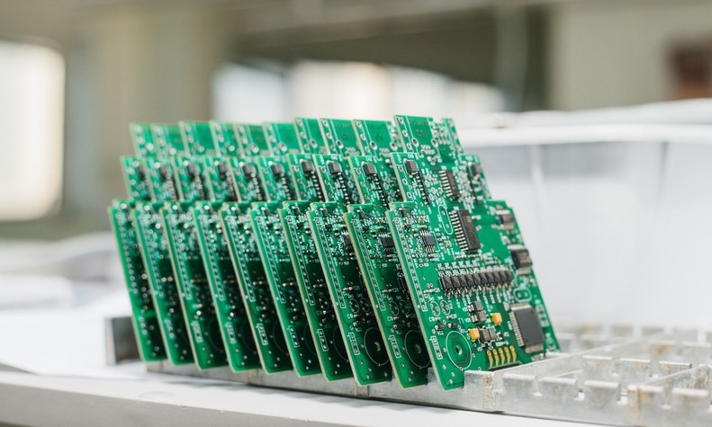
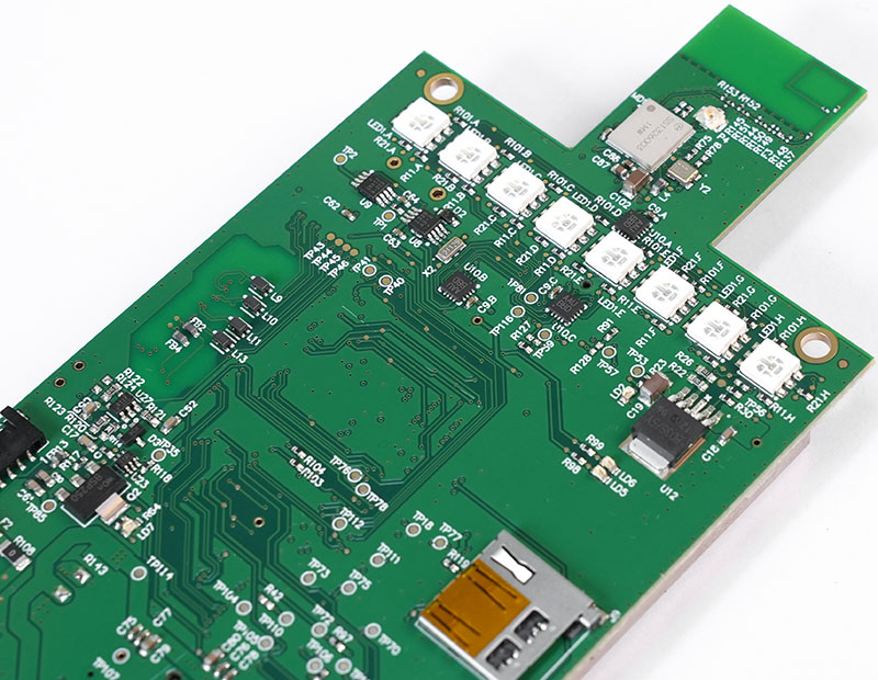
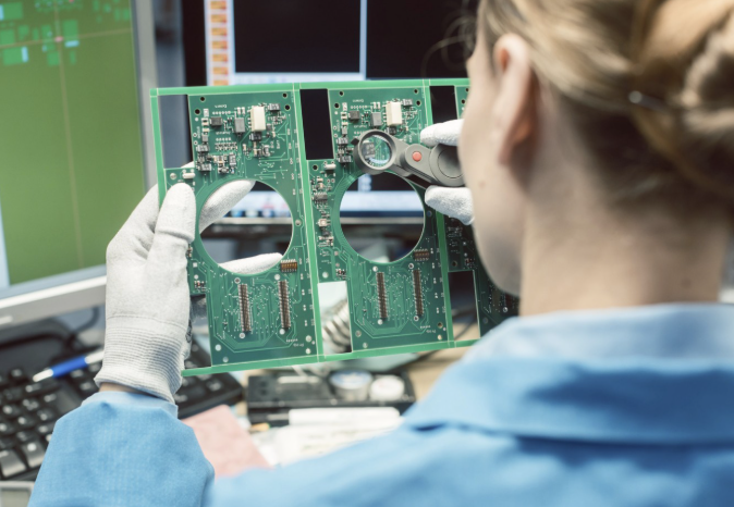
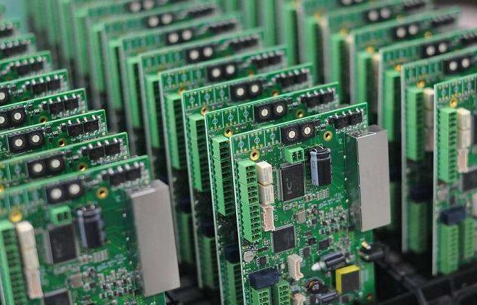
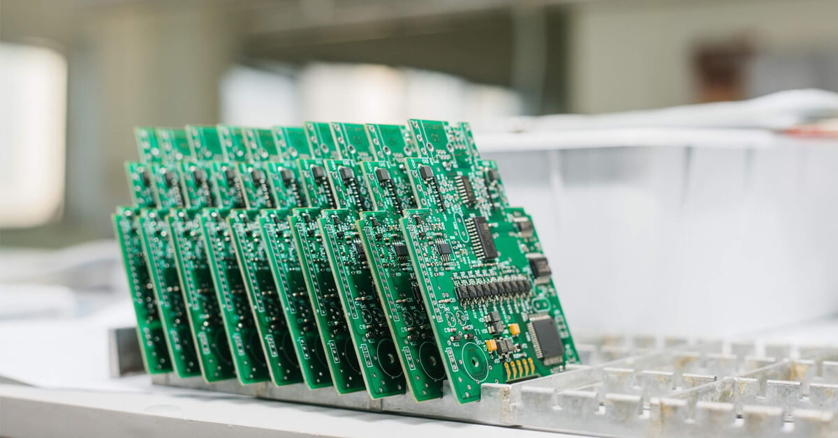
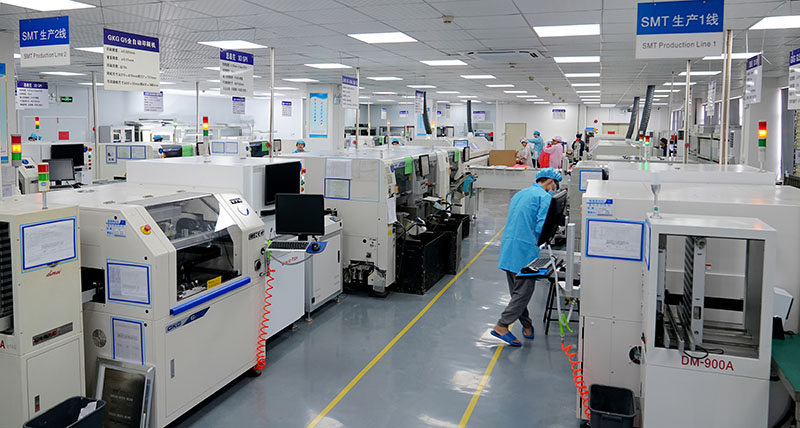
At EBest Circuit (Best Technology), we are a specialized provider of turnkey PCBA manufacturing services for the medical industry. Our core strength lies in a deeply engineered SMT PCBA process built on precision equipment, statistically controlled workflows, and a quality-first culture. Our SMT production capability is defined by advanced pick-and-place platforms, tightly controlled process flows, and rigorously validated engineering parameters—ensuring every assembly stage meets the stability and repeatability required for medical-grade manufacturing. For a consultation on your next project, contact our team at sales@bestpcbs.com.
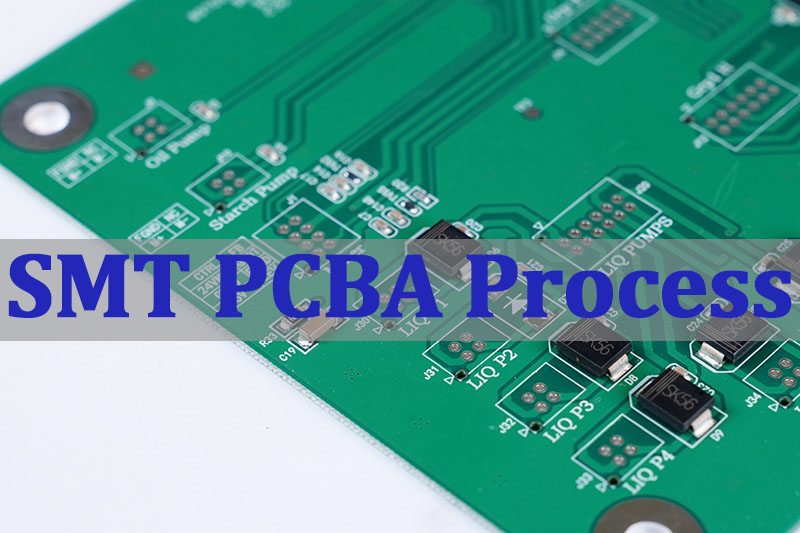
What Is The SMT PCBA Process?
The SMT PCBA process refers to the sequence of operations used to populate a bare PCB with electronic components using Surface Mount Technology (SMT). It is the dominant method for high-density, high-volume electronics assembly, including critical medical devices. This process involves applying solder paste, precisely placing components, and using controlled heat to form permanent solder joints. A well-controlled SMT process flow is characterized by repeatability, high yield, and the ability to handle increasingly miniaturized components. For a reliable turnkey medical project, understanding and controlling this process is non-negotiable.
The SMT assembly sequence is commonly broken into three major phases:
- Pre-Assembly: This includes all preparatory steps: solder paste printing (stencil application), adhesive dispensing (if needed for mixed-technology boards), and the critical setup and programming of the SMT pick and place machine.
- Assembly: The core phase where components are placed onto the pasted PCB. This stage is defined by the speed and accuracy of the automated placement equipment.
- Post-Assembly: This encompasses the soldering process (typically reflow soldering), cleaning (for no-clean or water-soluble pastes), and a series of inspections (Automated Optical Inspection – AOI, X-ray Inspection – AXI) to verify quality before any PCBA plug-in assembly of through-hole parts.
In summary, the SMT PCBA process is a sophisticated, phased manufacturing methodology that transforms a bare board into a functional assembly. Its effectiveness directly determines the performance, reliability, and longevity of the final electronic product, especially in life-critical medical applications.
SMT PCBA Process Step By Step Explained
A reliable SMT assembly follows a defined sequence where each step builds upon the quality of the previous one. For medical projects, consistency at every stage is paramount. Here is a detailed breakdown of a standard SMT PCBA process step by step:
- Solder Paste Printing: A stainless steel stencil is aligned over the PCB, and solder paste is deposited onto the solder pads. The quality of this print, including volume, alignment, and definition, is the first critical determinant of soldering success.
- Solder Paste Inspection (SPI): An inline 3D SPI system measures the height, volume, and area of each solder paste deposit. This real-time feedback allows for immediate correction of printing defects, preventing a cascade of failures later.
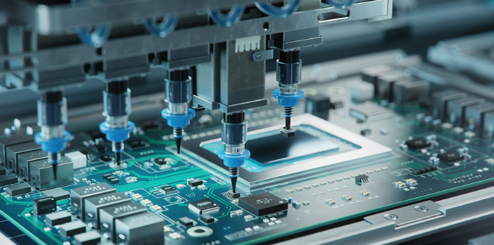
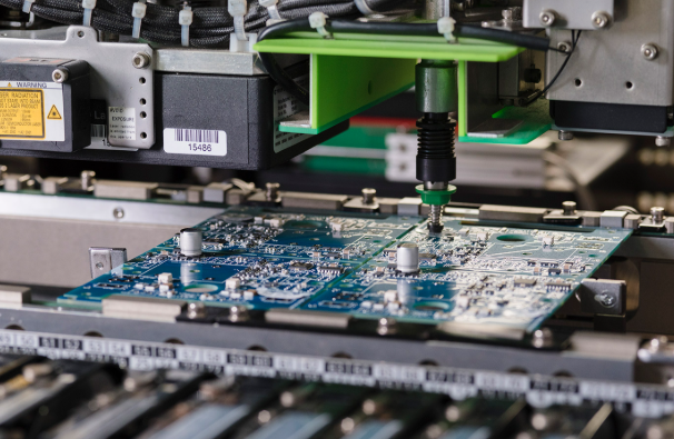
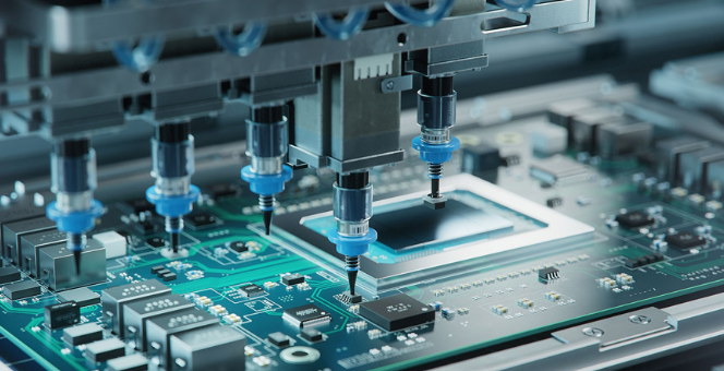
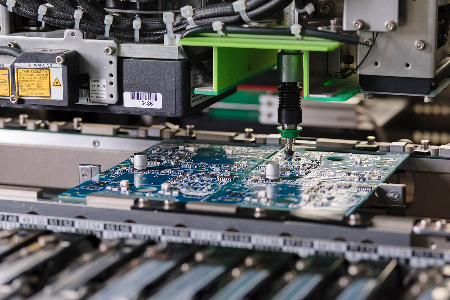
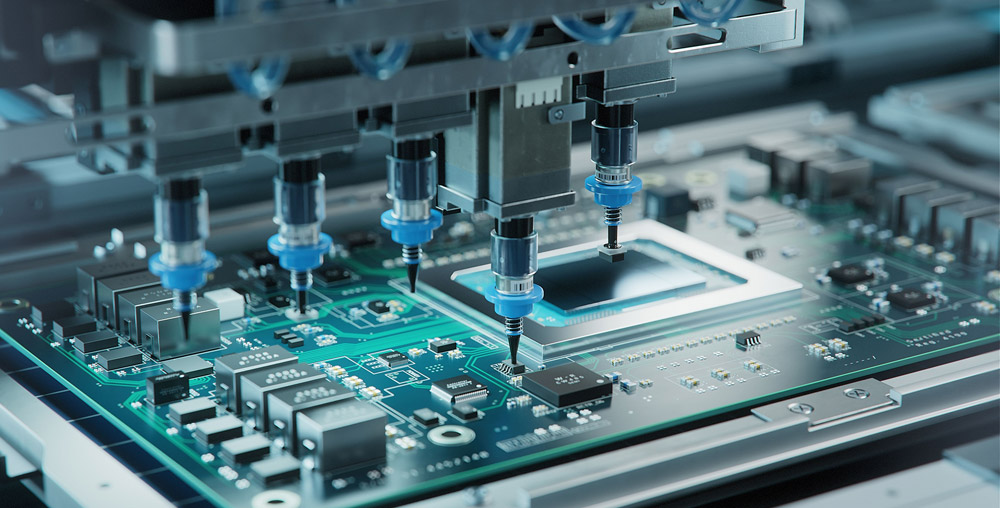
- Component Placement: The PCB moves to the SMT pick and place machine. Components from reels, trays, or tubes are picked up, optically centered, and placed with micron-level accuracy onto their corresponding solder paste deposits.
- Reflow Soldering: The populated board travels through a multi-zone reflow oven on a conveyor. A precise thermal profile melts the solder paste, forms intermetallic bonds, and then cools to create solid, reliable electrical and mechanical connections.
- Automated Optical Inspection (AOI): Post-reflow, an AOI system uses high-resolution cameras to check for placement errors, missing components, polarity issues, and visible solder joint defects.
- X-Ray Inspection (AXI): For medical assemblies with hidden solder joints (e.g., under BGAs or QFNs), AXI is essential. It verifies internal solder ball integrity, voiding percentage, and alignment, which are critical for long-term reliability.
- Conformal Coating & Final Assembly: For medical devices requiring protection from moisture and contaminants, a conformal coating may be applied. Finally, any necessary PCBA plug-in assembly of through-hole components is completed.
This step-by-step SMT PCBA process flow, when executed with precision equipment and strict controls, forms the foundation of a manufacturing line capable of producing medical-grade electronics with the required traceability and zero-defect mindset.
How Does The SMT Automation Process Work?
SMT automation is the backbone of modern medical PCBA manufacturing, enabling the speed, placement accuracy, and process repeatability required for regulated devices. Rather than isolated machines, automation links equipment, software, and data into a synchronized production system that minimizes variability and maximizes control.
At the core of this system is the SMT pick and place platform, supported by automated material handling, closed-loop process control, and centralized data management. Together, these elements form a fully integrated SMT production line designed for consistency, traceability, and validation readiness.
Key Elements of SMT Automation
- Material Handling
Automated loaders and unloaders feed bare boards into the line and remove completed assemblies, enabling continuous, stable operation with minimal manual intervention. - Pick and Place Operations
High-speed and high-precision placement heads handle components ranging from 0201 passives to fine-pitch BGAs, using advanced vision systems for fiducial alignment and placement correction. - Process Linking
Conveyor systems synchronize printers, SPI, placement machines, reflow ovens, and inspection stations into a single, balanced production flow. - Data Integration
A Manufacturing Execution System (MES) tracks each PCB in real time, associating it with feeder setup, stencil ID, reflow profile, and inspection results to form a complete digital record.
Key Automation Technologies in an SMT Line
| Technology | Primary Function | Medical Manufacturing Impact |
|---|---|---|
| 3D SPI | Paste volume verification | Early defect prevention |
| High-Precision Placers | Accurate micro-component placement | Supports miniaturized designs |
| Closed-Loop Reflow | Stable thermal control | Consistent solder reliability |
| AOI / AXI | Automated defect detection | Objective quality evidence |
In practice, SMT automation works as a closed-loop, data-driven environment. Inspection results feed back into placement and printing parameters, while MES data enables statistical process control and full traceability. This structure reduces human variability, stabilizes yield, and generates the documentation foundation required for SMT process validation and regulatory compliance in medical device manufacturing.
What Engineering Controls Ensure A Stable SMT Production Line?
For medical SMT PCBA processing, stability is synonymous with safety. Engineering controls are the documented procedures, specifications, and monitoring systems that prevent process drift and ensure every unit meets specification. A stable line is not achieved by chance but through deliberate, scientific control.
- Standardized Operating Procedures (SOPs): Every machine operation and manual task, from stencil cleaning to feeder setup, is governed by a detailed SOP. This eliminates variability between operators and shifts.
- Preventive Maintenance (PM) Schedules: Strict, calendar-based maintenance is performed on all critical equipment (printers, placers, ovens). This prevents unplanned downtime and ensures machines consistently perform within specification.
- Statistical Process Control (SPC): Key parameters are monitored in real-time using control charts. Examples include solder paste volume (from SPI), placement accuracy, and reflow oven temperatures. SPC signals trends before they become defects.
- Process Capability Studies (Cp/Cpk): These statistical measures quantify how well a process (e.g., solder paste printing) can meet its specified tolerance limits. A high Cpk (>1.33 is typical, >1.67 for critical characteristics) indicates a stable, capable process.
- Comprehensive Traceability: A lot-tracking system records the specific materials (paste lot, component reel), machine programs, and operator for every board or panel. This allows for targeted containment and root cause analysis if an issue arises.
- Environmental Controls: Temperature and humidity in the production area are controlled. Solder paste and moisture-sensitive devices (MSDs) are stored and handled according to strict protocols (e.g., IPC/JEDEC J-STD-033).
These engineering controls transform an SMT line from a collection of machines into a predictable, reliable manufacturing system. They are the tangible manifestations of a quality management system like ISO 13485 and are essential for passing audits and ensuring the long-term reliability of medical devices.
What Are Common PCBA Defects In SMT Assembly?
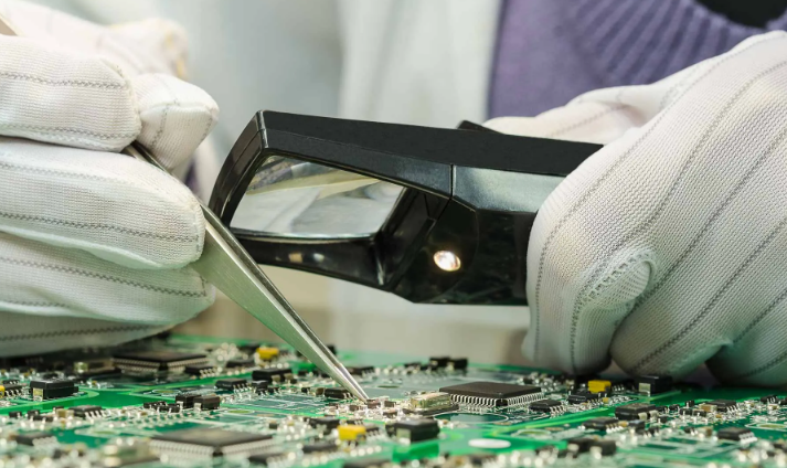
Even with a well-tuned process, defects can occur. Understanding their root causes is the first step to prevention. For ODM SMT PCBA rapid patch processing providers, rapid diagnosis and correction are key. Common defects include:
- Solder Bridging (Short): Solder inadvertently connects two adjacent pins or pads. Often caused by excessive solder paste, poor stencil design, or incorrect reflow profile.
- Tombstoning: A passive component (like a resistor or capacitor) stands up on one end. Typically caused by unequal solder paste volume or thermal mass on the two pads.
- Insufficient Solder (Open): A solder joint lacks sufficient material to form a reliable connection. Can result from poor paste printing, pad contamination, or an incorrect reflow profile.
- Component Misalignment: A part is offset or rotated from its intended position. Usually a fault of the pick and place machine’s calibration, vision system, or poor fiducial recognition.
- Voiding (in BGA joints): Gas bubbles trapped within a BGA solder ball. While some voiding is acceptable per IPC standards, excessive voids can weaken the joint and impact thermal performance. Often related to paste chemistry or reflow profile.
- Cold Solder Joint: A joint that appears dull, grainy, and has not properly fused. Caused by insufficient heat during reflow or contamination.
Root Cause & Corrective Action (RCCA) for Defects:
A stable medical SMT line relies on immediate defect detection (via AOI/AXI) and systematic RCCA. For example, a spike in bridging defects would trigger an investigation of the stencil’s condition, the printer’s settings, and the recent reflow oven profile, ensuring the issue is corrected at its source.
What Is CPK In SMT Manufacturing Process Control?
Cpk (Process Capability Index) is a crucial statistical measure in SMT process control. It quantifies how well a controlled process can consistently produce outputs within the specified tolerance limits. In simple terms, it tells you if your process is centered and precise enough.
- The Concept: Every process has natural variation. Cpk compares the spread of this natural variation (process width) to the distance between the specification limits (customer/engineering requirements). A higher Cpk indicates the process is well-centered and has a smaller spread relative to the limits, meaning a lower probability of defects.
- Formula: Cpk = min[ (USL – μ) / 3σ , (μ – LSL) / 3σ ]
- USL/LSL: Upper/Lower Specification Limit
- μ: Process mean (average)
- σ: Process standard deviation (variation)
- Interpretation in SMT:
- Cpk < 1.0: The process spread is too wide and/or not centered. It is incapable of consistently meeting specs. Immediate corrective action is required. (e.g., Solder paste height is too variable).
- Cpk ≥ 1.33: The process is considered capable. This is a common industry minimum.
- Cpk ≥ 1.67: The process is highly capable and robust. This is the target for critical characteristics in medical SMT PCBA processing, such as solder paste volume or reflow peak temperature.
For a medical device manufacturer, reporting Cpk values for key processes (paste printing, placement accuracy) is a powerful demonstration of a mature, stable, and statistically validated production line. It moves quality assurance from a “check-the-box” inspection to a predictive science.
What Is The PiP Process In SMT Assembly?
PiP (Pin-in-Paste), also known as Paste-in-Hole or Intrusive Reflow, is a hybrid assembly technique that allows through-hole components to be soldered during the SMT reflow process. This simplifies assembly by eliminating a separate wave soldering or manual soldering step, which is valuable for turnkey projects seeking efficiency.
How it works:
- The PCB goes through the standard solder paste printing process.
- Solder paste is deposited not only on SMD pads but also into the plated through-holes (PTHs) intended for PiP components.
- SMT components are placed as usual.
- PiP components (typically connectors or larger electromechanical parts with long leads) are inserted into the paste-filled holes. This can be done manually or with automated insertion equipment.
- The entire assembly then passes through the reflow oven. The solder paste in the PTHs melts, flows, and creates a fillet, soldering the PiP component in place.
Advantages for Medical PCBA:
- Process Simplification: Reduces the number of soldering stages, lowering cost and cycle time.
- Improved Reliability: Can create more robust solder joints for heavy components compared to wave soldering.
- Design Flexibility: Useful for mixed-technology boards where a few through-hole parts are needed alongside dense SMT.
Considerations:
Successful PiP requires careful design (adequate PTH size, solder paste volume calculation), specialized stencil design, and process validation to ensure complete hole fill and avoid solder voids.
How Is SMT Process Validation Performed In Mass Production?
SMT process validation is a formal, documented procedure that provides high confidence that a specific SMT process will consistently produce a PCBA meeting all predetermined quality and regulatory requirements. For mass production of medical devices, it is a mandatory gate before commercial launch.
The validation follows a structured, three-phase approach often aligned with the Installation Qualification (IQ), Operational Qualification (OQ), and Performance Qualification (PQ) framework.
- Installation Qualification (IQ): Verifies that the SMT production line equipment (printer, SPI, placer, oven) is correctly installed according to manufacturer specifications and site requirements. This includes checking utilities, calibrations, and software versions. Documentation: Equipment manuals, calibration certificates, installation checklists.
- Operational Qualification (OQ): Demonstrates that the installed equipment can operate consistently within established limits and tolerances under “worst-case” scenarios. This involves running the machines with test programs and challenging conditions.
- Example OQ Tests:
- Printer: Repeatability of paste volume across multiple prints.
- Placer: Accuracy and repeatability of placement using a test board.
- Reflow Oven: Verification of thermal profile consistency across all zones and across the conveyor width.
- Example OQ Tests:
- Performance Qualification (PQ): Also known as Process Validation, this is the most critical phase. It proves that the entire, integrated process, using production-intent materials, can consistently produce acceptable product.
- A validation lot (typically 3 consecutive production runs) is manufactured.
- The entire SMT PCBA process flow is executed under standard operating procedures.
- Every unit is subjected to comprehensive inspection and testing (visual, AOI, AXI, functional test).
- Data is collected and analyzed to prove the process is stable and capable (using statistical tools like Cpk).
- The outcome is a definitive report stating whether the process is validated for mass production.
For a medical device manufacturer, a completed validation package is a cornerstone of the Design History File (DHF) and is essential for regulatory submissions to bodies like the FDA. It is the ultimate proof that the manufacturing process is under control.
In summary, the SMT PCBA process is a complex yet precisely engineered sequence that forms the critical link between electronic design and a reliable, manufacturable medical device. Mastering this process—from the SMT process flow chart to real-time process control with metrics like CPK—is what separates a basic assembler from a qualified medical manufacturing partner.
This article has detailed the steps, controls, and validation frameworks necessary to achieve the reliability demanded by turnkey medical projects. Success hinges on automation, data-driven engineering, and a culture of continuous improvement.
At EBest Circuit (Best Technology), we have built our service around this principle. Our professional ODM SMT PCBA rapid patch processing is supported by a SMT production line equipped with advanced inspection technology and governed by a strict ISO 13485 quality system. We understand that for medical devices, the process isthe product. Pls feel free to contact our engineering team anytime at sales@bestpcbs.com to discuss your project requirements.
FAQs
How Is A PCBA Different From A PCB?
A PCB (Printed Circuit Board) is the bare, unpopulated board—just the laminate, copper traces, and solder mask. A PCBA (Printed Circuit Board Assembly) is the completed, functional board after all electronic components (SMT and/or through-hole) have been soldered onto it. The SMT PCBA process is what transforms a PCB into a PCBA.
What Is The Difference Between PCB And SMT?
This is a common point of confusion. PCB refers to the physical board itself. SMT (Surface Mount Technology) refers to one of the primary methods used to assemble components onto that PCB. SMT is a PCB assembly process, not the board.
How Do SMT Assembly Services Handle Component Availability?
Professional ODM SMT PCBA rapid patch processing partners manage this proactively. They maintain long-term relationships with franchised distributors, use component market analysis tools to forecast shortages, and offer DFM (Design for Manufacturability) reviews early in the design phase to suggest alternates for parts at risk of obsolescence, which is vital for the long lifecycles of medical devices.
What SMT Component Sizes Are Hardest To Assemble?
The greatest challenges come at the extremes of miniaturization: 01005 (0.4mm x 0.2mm) and smaller passive components, and ultra-fine-pitch components (e.g., 0.3mm pitch BGAs or CSPs). These require ultra-high-precision SMT pick and place machines, specialized stencil designs, and exquisite process control to avoid defects like bridging or misplacement.
What Are Typical Turnaround Times For SMT Assembly Services?
Turnaround time depends on project complexity, layer count, component sourcing, and quantity. For a standard prototype run with all parts in stock, rapid patch processing can be as quick as 24-72 hours for SMT assembly. For new medical projects requiring full process validation and regulatory documentation, the initial timeline will be longer to ensure quality, with subsequent production runs following a predictable schedule.