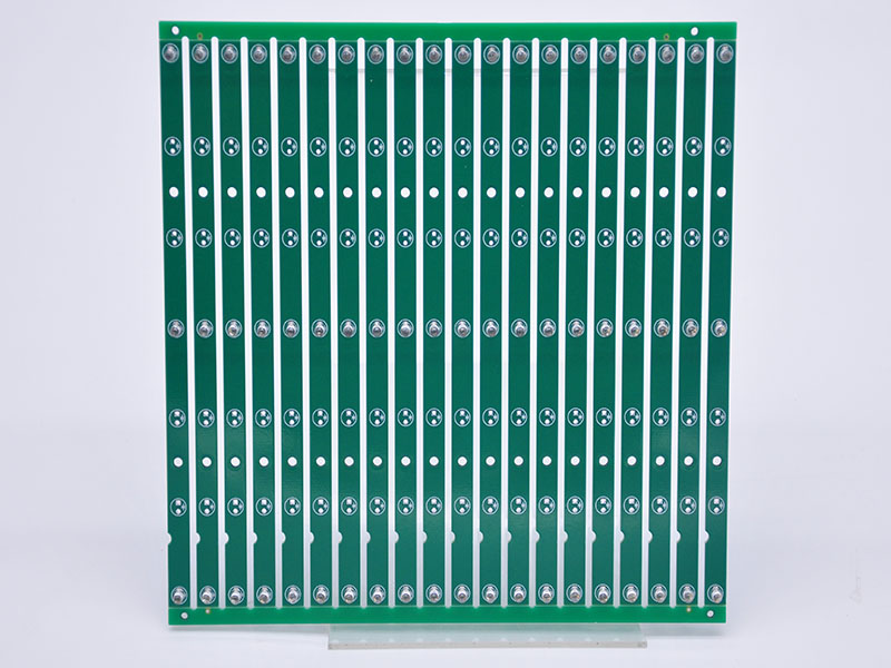
A south-facing PCB refers to a printed circuit board designed to accommodate south-facing switches, where the LED hole of each switch faces the bottom of the PCB (and toward the user when installed). This design is critical for keycap compatibility and lighting performance, making the south-facing PCB a top choice for custom mechanical keyboards and specialized electronic devices. Whether you’re building a custom keyboard or designing components for industrial equipment, understanding south-facing PCB nuances ensures optimal performance and user experience.
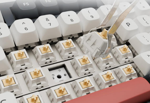
What Is a South-Facing PCB and How Does It Work?
A south-facing PCB is defined by its switch mounting orientation: the LED aperture on each switch socket faces the bottom edge of the PCB. When switches are soldered or hot-swapped onto the board, this orientation positions the LED below the keycap rather than above it. This setup avoids interference with Cherry-profile keycaps—one of the most popular keycap designs—preventing the keycap stem from colliding with the LED. The PCB’s trace routing and pad placement are optimized to support this orientation, ensuring stable electrical connections and compatibility with standard switch footprints.
South-Facing vs. North-Facing PCB: What’s the Difference?
| Feature | South-Facing PCB | North-Facing PCB |
|---|---|---|
| LED Orientation | Faces bottom of PCB (toward user) | Faces top of PCB (away from user) |
| Keycap Compatibility | Works with all profiles (no Cherry profile interference) | Cherry profile keycaps may collide with LEDs |
| RGB Lighting Performance | Dimmer legend backlighting; better side glow | Brighter legend backlighting; direct LED alignment |
| Typical Applications | Custom keyboards, industrial control panels | Gaming keyboards, RGB-focused devices |
| Switch Compatibility | Supports all standard MX-style switches | Same switch compatibility; LED position varies |
What Are the Advantages of a South-Facing PCB?
Keycap Versatility
The primary advantage of a south-facing PCB is universal keycap compatibility. It eliminates interference with Cherry, OEM, and DSA profiles, allowing users to customize their devices without fit issues. This is critical for custom keyboard builders and industrial equipment designers who require specific keycap ergonomics.
Stable Typing Experience
By avoiding keycap-stem collisions, south-facing PCBs deliver a smoother typing feel with consistent switch actuation. This stability is essential for medical devices like diagnostic equipment, where precise input is non-negotiable.
Design Flexibility
South-facing PCBs support hot-swappable and soldered switch configurations, offering flexibility for prototyping and production. This adaptability makes them suitable for aerospace components, where design iterations and reliability are paramount.
What Industries Use South-Facing PCBs?
Medical Equipment
Medical devices like patient monitors and diagnostic keyboards rely on south-facing PCBs for reliable input and keycap compatibility. A leading medical equipment manufacturer integrated our south-facing PCB into their portable ultrasound machines, ensuring clinicians can use sterile, custom keycaps without performance issues.
Aerospace
Aerospace control panels use south-facing PCBs for their durability and design flexibility. Our south-facing PCB was adopted in a commercial aircraft’s in-flight entertainment system, supporting rugged keycaps and stable operation in extreme pressure and temperature conditions.
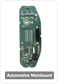
Industrial Equipment
Industrial control terminals and machinery interfaces benefit from south-facing PCBs’ keycap versatility. A manufacturing client used our PCBs in assembly line control panels, allowing workers to use wear-resistant keycaps without interfering with switch functionality.
How to Design a South-Facing PCB for Optimal Performance?
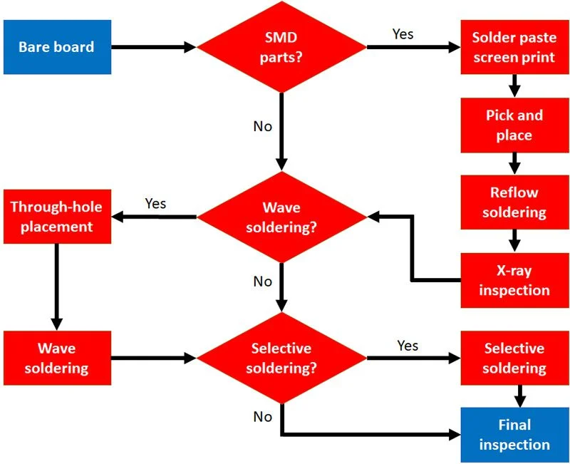
Start by selecting switch footprints compatible with south-facing orientation (MX-style is standard). Ensure LED pads are positioned at the bottom of each switch socket, with trace routing that avoids signal interference. Incorporate ground planes to enhance signal integrity, critical for high-speed industrial and aerospace applications. Conduct design rule checks (DRC) to verify pad spacing and prevent short circuits, and test with sample keycaps to confirm no interference.
- Use 1oz-2oz copper for traces to support current demands
- Position LEDs 0.5mm below switch stems to avoid contact
- Integrate ESD protection for sensitive electronic environments
Common Issues with South-Facing PCBs and How to Fix Them?
Dim RGB Lighting
South-facing LEDs produce dimmer legend backlighting. Fix this by using high-brightness LEDs (3000mcd+) or dye-sublimated keycaps with translucent legends. For industrial devices, prioritize side glow over legend lighting if backlighting is non-essential.
Switch Installation Misalignment
Misaligned switches cause keycap wobble. Ensure PCB pads are precision-drilled (tolerance ±0.05mm) and use alignment jigs during assembly. This is critical for medical devices where input precision is critical.
Signal Interference
Poor trace routing leads to signal degradation. Use ground planes and separate analog/digital traces to minimize interference. For aerospace applications, conduct EMI testing to ensure compliance with industry standards.
FAQ About South-Facing PCBs
Can south-facing PCBs use north-facing switches? No—switches are orientation-agnostic, but the PCB’s LED pad position determines compatibility. South-facing PCBs work with standard MX-style switches; only the LED aperture direction differs.
Do south-facing PCBs support hot-swappable switches? Yes—many south-facing PCBs feature hot-swap sockets (e.g., Kailh) for tool-free switch replacement. This is ideal for custom keyboards and industrial prototyping.
Are south-facing PCBs more expensive than north-facing ones? No—cost is comparable, as the only difference is pad and LED placement. Pricing depends on materials (e.g., FR-4 vs. high-temperature substrates) and manufacturing complexity.
Can south-facing PCBs be used for gaming keyboards? Yes—though RGB performance is dimmer, gamers prioritizing keycap customization over bright backlighting prefer them. Some gaming keyboards use south-facing designs for Cherry profile compatibility.
How to test a south-facing PCB for LED functionality? Use a multimeter to check continuity between LED pads and traces. Power the PCB with a 5V source and verify LED illumination; dim legends are normal for south-facing orientations.
Are south-facing PCBs suitable for high-temperature environments? Yes—when manufactured with high-temperature substrates (e.g., polyimide), they perform reliably in aerospace and industrial settings with temperatures up to 150°C.
What Materials Are Best for South-Facing PCBs?
For most applications, FR-4 is the standard substrate due to its durability and cost-effectiveness. For medical and aerospace devices, use high-reliability materials like Rogers 4003C (for high-frequency signals) or polyimide (for flexibility and temperature resistance). Copper thickness (1oz-2oz) should match current demands, and solder mask in green or black ensures corrosion resistance.
How to Choose the Right South-Facing PCB for Your Project?
Consider your application’s needs: keycap compatibility (Cherry profile users need south-facing), lighting requirements (RGB vs. non-RGB), and environmental conditions (temperature, moisture). For industrial and medical projects, prioritize PCBs with ISO 13485 or IPC-6012 certification. Partner with a manufacturer that offers custom routing to match your switch layout and component placement.
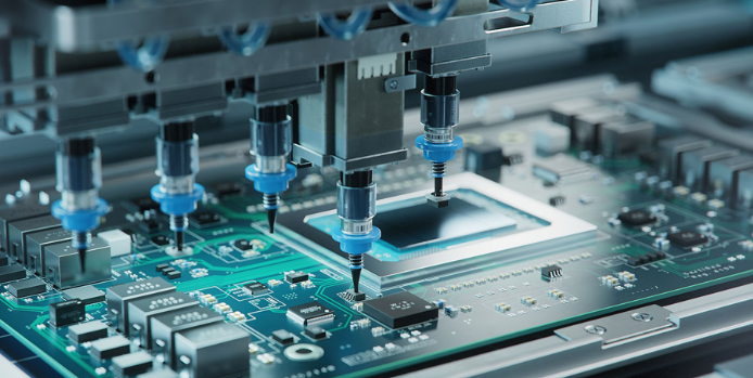
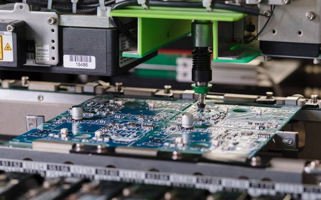
What Are the Best Practices for Assembling South-Facing PCBs?
Use lead-free solder (Sn96.5/Ag3.0/Cu0.5) for compliance with industrial standards. Avoid overheating switches during soldering (temperature ≤350°C, time ≤3 seconds) to prevent LED damage. Test keycap fit before final assembly to ensure no interference, and conduct continuity checks for all traces and LEDs. For hot-swappable PCBs, verify socket alignment to prevent switch wobble.
How Does ESD Protection Impact South-Facing PCBs?
Electrostatic discharge (ESD) can damage LEDs and switches on south-facing PCBs. Integrate ESD diodes (e.g., TVS diodes) near LED pads and switch sockets. For medical and aerospace applications, ensure surface resistance between 10⁶-10⁹Ω to dissipate static. Use conductive packaging during storage and assembly to prevent ESD-related failures.
What Trends Are Shaping South-Facing PCB Design?
Increased demand for custom mechanical keyboards drives innovations in south-facing PCB design, including hot-swappable sockets and integrated RGB controllers. Medical and aerospace industries are adopting smaller, more durable south-facing PCBs for portable devices. Advances in LED technology (micro-LEDs) are improving backlighting performance, addressing the dimness issue associated with south-facing orientations.
At EBest, we specialize in high-quality south-facing PCB manufacturing for medical, aerospace, and industrial applications. Our south-facing PCB products meet strict E-E-A-T standards, with custom design support for south-facing pcb design and tailored solutions for aerospace south-facing pcb and medical device south-facing pcb requirements. We also provide expert guidance for south-facing pcb assembly best practices and high-performance options for south-facing pcb for industrial equipment. Whether you need prototype batches or mass production, we deliver reliable, compatible south-facing PCBs tailored to your unique project needs. Contact us at sales@bestpcbs.com to place your order today.