Are you struggling with overheating, inconsistent quality, or unreliable performance from your VCU MCPCB for Automotive? EBest’s solution solves these core pain points with industry-leading specs and reliability. Below, we break down how our VCU MCPCB works, its key advantages, and how it keeps your automotive projects on track.

Why Choose EBest for Your Automotive VCU MCPCB Manufacturer?
EBest is your trusted partner for high-quality automotive VCU MCPCB solutions, designed to meet the strict demands of automotive vehicle control units. Our products combine superior performance, consistent quality, and timely delivery to keep your projects on track. Here are reasons why choose us for your automotive VCU MCPCB manufacturer:
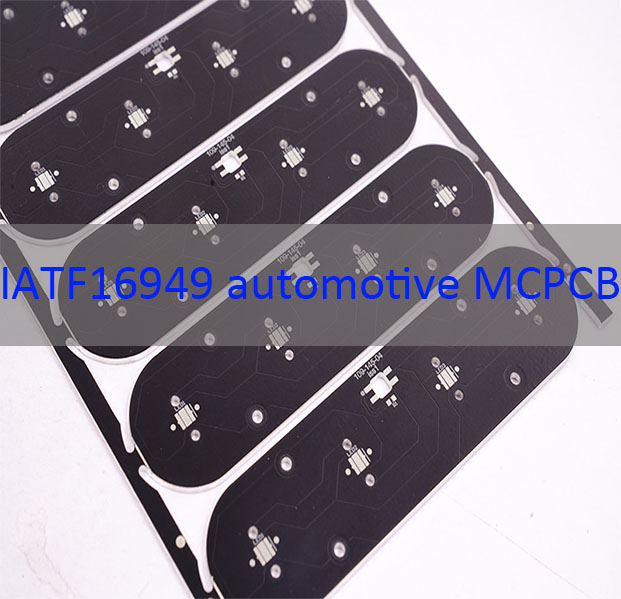
- Quality: Our VCU MCPCB undergoes rigorous testing to meet IATF 16949 and ISO 26262 standards, ensuring zero quality defects and long-term reliability in harsh automotive conditions.
- Delivery: We maintain a stable supply chain and efficient production process, guaranteeing on-time delivery even for large-volume orders, no delays to your project timeline.
- Cost-Efficiency: Our optimized manufacturing process reduces unnecessary waste, offering competitive pricing without compromising on performance or quality.
- Service: Our technical team provides 24/7 support, from design consultation to after-sales service, ensuring your VCU MCPCB integrates seamlessly into your VCU design.
- Supply Chain: We source high-grade materials from trusted global suppliers, minimizing supply chain risks and ensuring consistent product quality batch after batch.
What Are Common Pain Points with VCU MCPCB & How Does EBest Solve Them?
Many users face challenges with VCU MCPCB performance, manufacturing consistency, and supply stability. EBest addresses these pain points head-on with tailored solutions.
Pain Point 1: Poor heat dissipation leading to VCU overheating and failure.
Solution: Our VCU MCPCB uses high-thermal-conductivity dielectric layers (2.0-5.0 W/m·K) and metal bases to quickly dissipate heat, preventing component damage and ensuring long-term reliability.
Pain Point 2: Inconsistent quality between batches.
Solution: We implement strict quality control throughout production, from material inspection to final testing, adhering to IATF 16949 standards to ensure every VCU MCPCB meets the same high standards.
Pain Point 3: Delayed delivery disrupting project timelines.
Solution: Our streamlined production process and stable supply chain ensure on-time delivery, even for urgent orders, we prioritize your project’s schedule.
Pain Point 4: Poor signal integrity affecting VCU performance.
Solution: Our VCU MCPCB design optimizes layout to reduce crosstalk and interference, ensuring clear signal transmission for accurate VCU operation.
Pain Point 5: High production defects increasing costs.
Solution: We use advanced manufacturing techniques and strict process control to minimize defects, reducing waste and ensuring cost-efficiency for your business. Choose EBest for reliable, pain-free VCU MCPCB solutions.
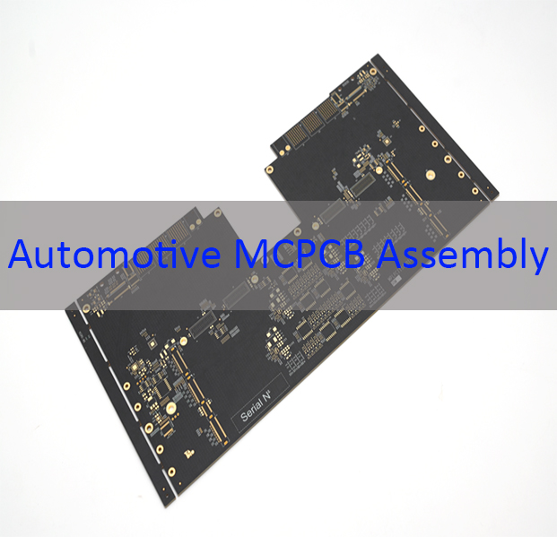
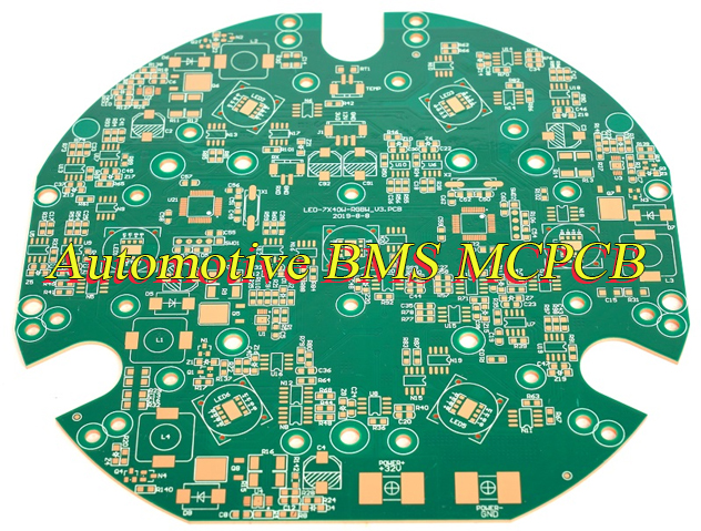
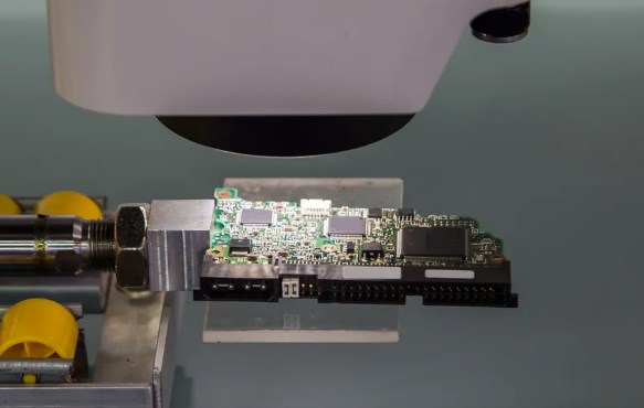
What Is VCU MCPCB & Why Is It Critical for Automotive Vehicle Control Units?
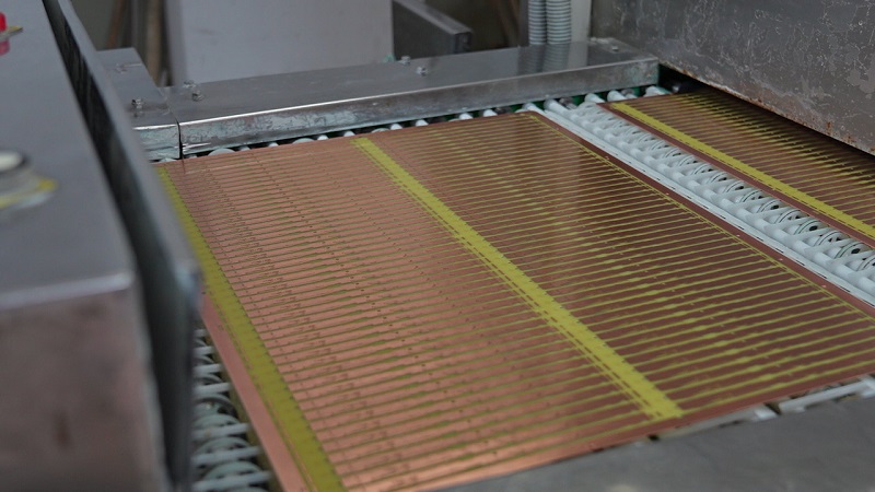
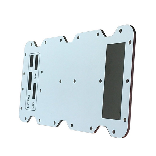
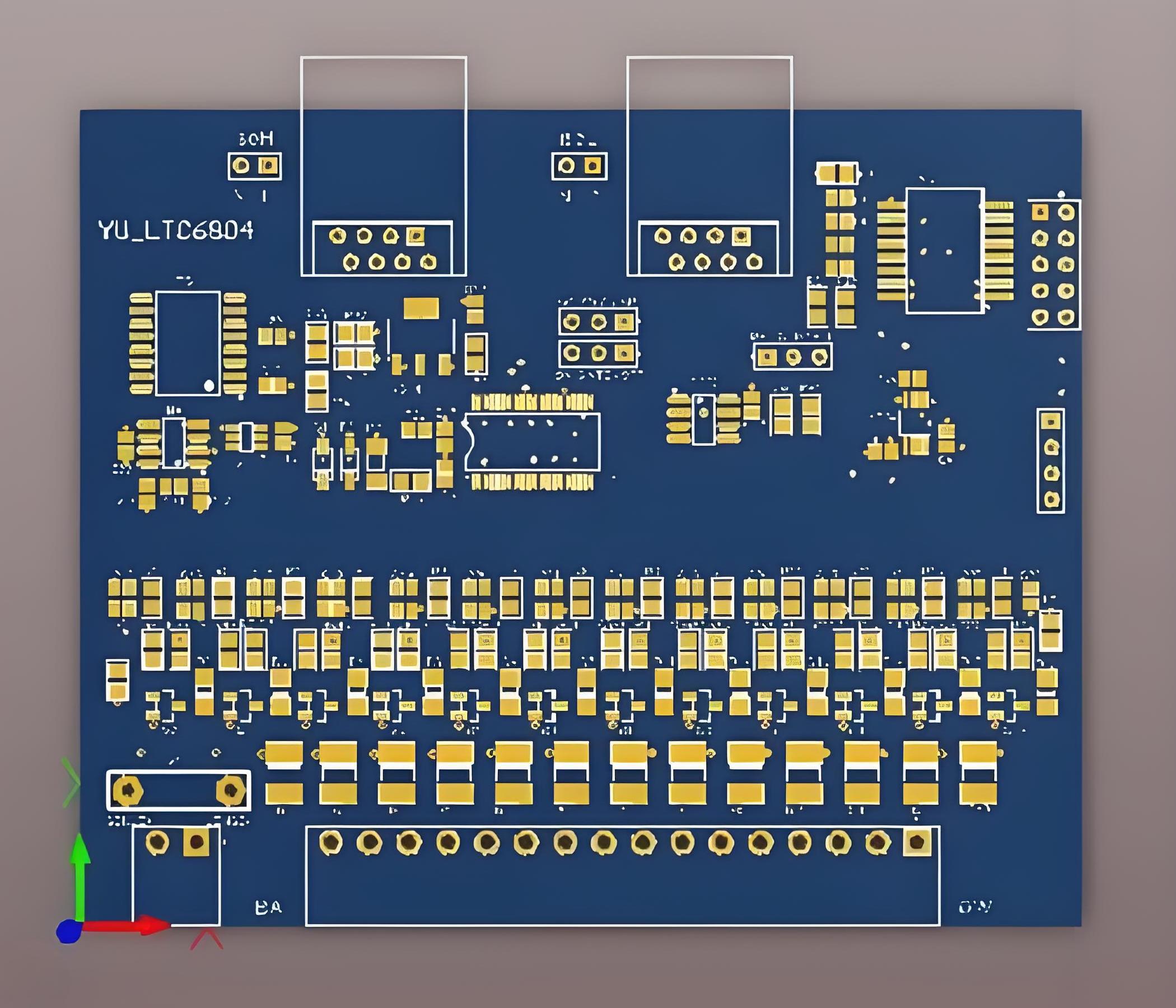
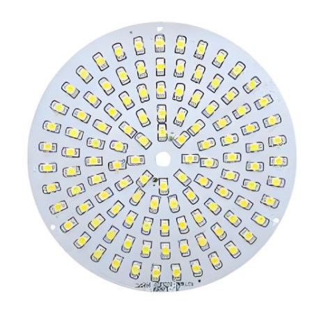
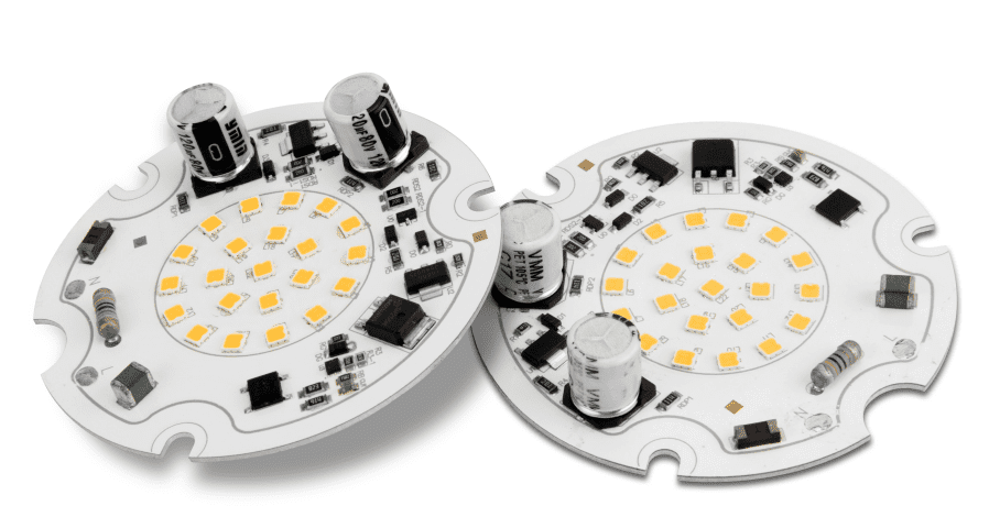
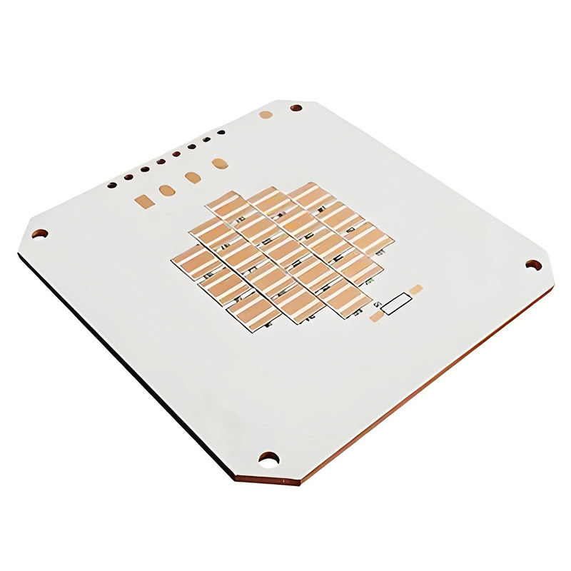
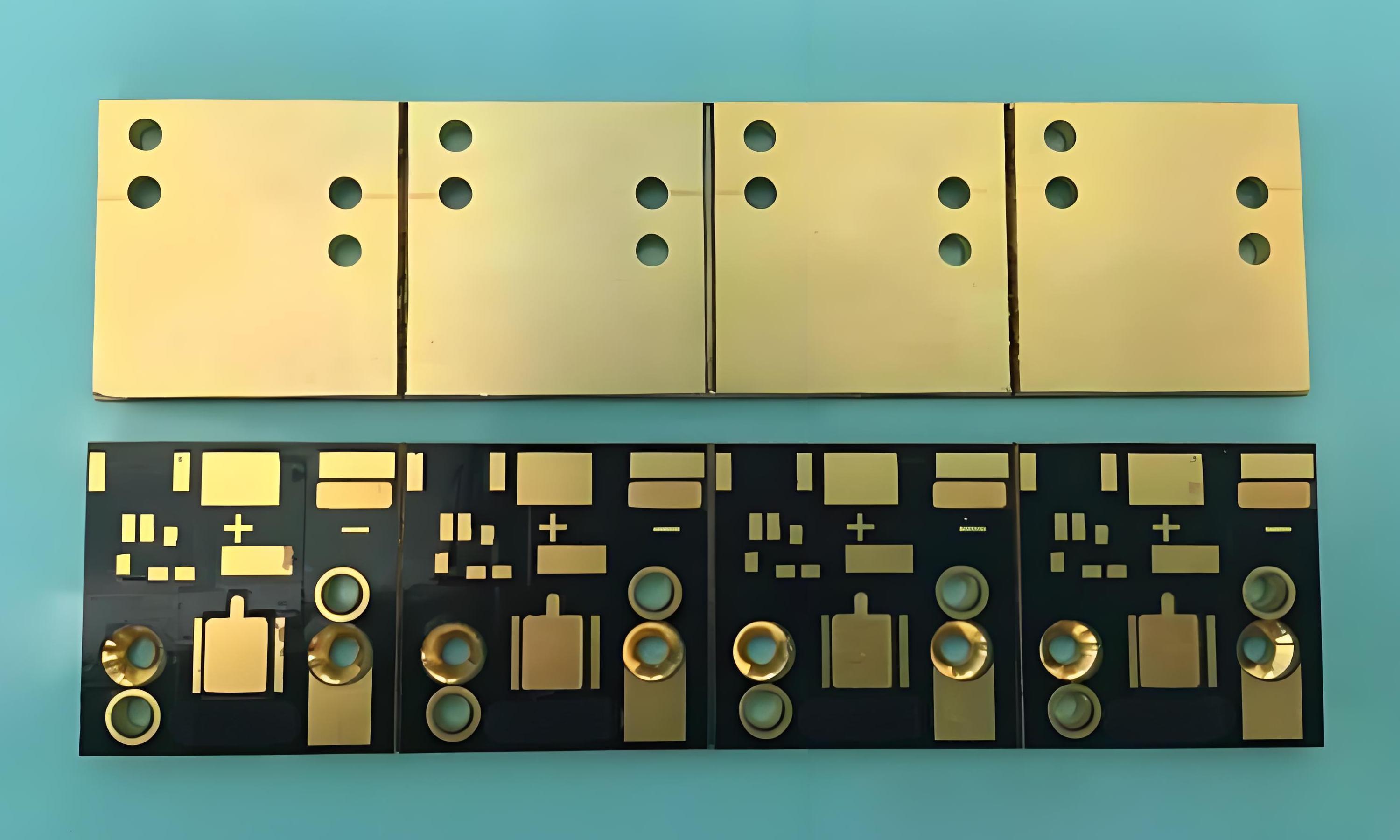
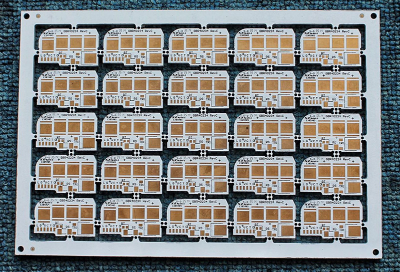
VCU MCPCB, or Vehicle Control Unit Metal Core Printed Circuit Board, is a specialized circuit board crafted specifically for automotive VCUs. It features a three-layer structure, copper circuit layer, thermally conductive dielectric layer, and metal core—that sets it apart from standard PCBs, making it ideal for the demanding conditions of automotive applications.
Automotive VCUs act as the central “brain” of electric and hybrid vehicles, managing critical functions like power distribution, motor control, and battery management. These operations generate significant heat, and standard PCBs lack the thermal management capabilities to dissipate this heat effectively, leading to component damage and premature VCU failure.
This is where VCU MCPCB becomes critical. Its metal core, typically made of aluminum or copper, acts as a built-in heat spreader to draw heat away from sensitive components, ensuring stable performance in extreme under-hood temperatures. A high-quality VCU MCPCB directly safeguards vehicle safety and reliability, making it an indispensable component for modern automotive electronics.
How Does VCU MCPCBs Improve Thermal Management in Automotive VCUs?
VCU MCPCB improves thermal management through its unique three-layer structure: copper circuit layer, dielectric layer, and metal core, each designed to enhance heat transfer.
The metal core (aluminum or copper) has excellent thermal conductivity, acting as a heat spreader to disperse heat across the board. The dielectric layer, with high thermal conductivity (2.0-5.0 W/m·K), transfers heat from the copper layer to the metal core without electrical interference.
This design ensures heat is quickly removed from VCU components, keeping operating temperatures within safe limits. Compared to traditional FR-4 PCBs, VCU MCPCB reduces component temperature by 30-50%, significantly extending VCU lifespan and reliability.
What Certifications Does EBest’s VCU MCPCB Have?
EBest’s VCU MCPCB holds industry-leading certifications, ensuring compliance with global automotive standards and providing tangible value for your business. Below is a detailed breakdown of our certifications and their benefits:
- IATF 16949: Maintains strict control over production processes to eliminate quality risks, ensuring our products align with global automotive supply chain expectations.
- ISO 26262: Delivers critical functional safety, minimizing the risk of vehicle control unit failures and ensuring adherence to automotive safety protocols.
- ISO 9001:2015: Validates our consistent quality management system, so you can trust that every unit meets your exact specifications, batch after batch.
What Are the Key Specifications to Look for in a High-Quality VCU MCPCBs?
When choosing a VCU MCPCB, focus on these critical specifications to ensure it meets automotive VCU requirements and delivers long-term reliability. Below is a clear breakdown of key specifications and their standard ranges:
| Specification | Standard Range |
| Thermal Conductivity | 2.0 – 5.0 W/m·K |
| Operating Temperature Range | -40℃ to 125℃ |
| Dielectric Strength | ≥15 kV/mm |
| Copper Thickness | 1 oz – 4 oz |
| Metal Base Material | Aluminum or Copper |
| Automotive Certifications | IATF 16949, ISO 26262, AEC-Q100 |
What Automotive VCU Applications Benefit Most from EBest’s VCU MCPCB?
EBest’s VCU MCPCB is designed for all automotive VCU applications, particularly those requiring high reliability and heat dissipation. Key applications include:
- Electric Vehicle (EV) VCUs: Manages battery charging, motor control, and power distribution, requiring efficient heat dissipation for continuous operation.
- Hybrid Electric Vehicle (HEV) VCUs: Balances internal combustion engine and electric motor performance, operating in high-temperature environments.
- Commercial Vehicle VCUs: Withstands heavy vibrations and extreme temperatures, ensuring reliable performance in trucks and buses.
- Autonomous Vehicle VCUs: Supports high-power computing and sensor integration, requiring stable performance and minimal signal interference.
- Off-Road Vehicle VCUs: Resists dust, moisture, and extreme temperature fluctuations, ensuring durability in harsh off-road conditions.
How to Design a VCU MCPCB for Optimal Performance in Automotive Applications?
Designing a VCU MCPCB for automotive applications requires careful consideration of heat dissipation, signal integrity, and durability. Follow these key steps for optimal performance:
- Choose the Right Thermal Conductivity: Select a dielectric layer with 2.0-5.0 W/m·K thermal conductivity to match your VCU’s heat output. Higher heat-generating VCUs (e.g., EV powertrain VCUs) require higher thermal conductivity.
- Optimize Layout for Heat Dissipation: Place high-heat components (e.g., power MOSFETs, microcontrollers) directly above the metal core to maximize heat transfer. Use wide copper traces to reduce heat buildup.
- Ensure Signal Integrity: Separate analog and digital signals to reduce crosstalk. Use differential routing for CAN/CAN FD signals, and keep high-speed traces short to minimize interference.
- Select the Right Metal Base: Choose aluminum for cost-effective, lightweight designs, or copper for high-heat applications. Ensure the metal base thickness (30-125 mil) provides sufficient mechanical stability.
- Comply with Automotive Standards: Design to IATF 16949 and ISO 26262 standards, ensuring your VCU MCPCB meets the safety and reliability requirements of automotive applications.
What Is the Real-World Performance of EBest’s VCU MCPCB in Automotive Applications?
EBest’s VCU MCPCB has been tested and proven in real automotive applications, solving critical performance issues for our clients. Here’s a detailed case study:
Case Study: EV VCU Overheating Solution
A leading EV manufacturer faced frequent VCU failures due to overheating. Their existing FR-4 PCB could not dissipate heat from the high-power microcontroller (NXP MPC5744), leading to component damage and production delays.
EBest provided a VCU MCPCB with 3.0 W/m·K thermal conductivity, aluminum base, and optimized layout. The solution reduced the microcontroller’s operating temperature by 40℃, eliminating overheating failures.
The client reported zero VCU failures after implementing our VCU MCPCB, improving production efficiency and reducing warranty costs. Our solution also met IATF 16949 and ISO 26262 standards, ensuring compliance with global automotive requirements.
How Does EBest Ensure Consistent Quality for VCU MCPCB Batches?
Consistent quality is critical for VCU MCPCB, as batch-to-batch variations can lead to VCU failures and project delays. EBest implements a multi-step quality control process to guarantee consistency across every batch:
- Strict Raw Material Inspection: All raw materials (metal core, copper foil, dielectric layer) undergo thorough testing for thermal conductivity, thickness, and durability before entering production. This ensures only high-grade materials are used, laying the foundation for consistent quality.
- Real-Time In-Process Testing: Key production steps—including lamination, etching, and drilling are closely monitored to maintain process stability. Standardized procedures and automated systems help reduce variability, preventing defects during manufacturing.
- Comprehensive Final Testing: Every VCU MCPCB undergoes thermal, electrical, and mechanical testing to verify performance and compliance with specifications. This includes automated optical inspection (AOI) and functional testing to catch any potential issues before shipping.
- Full Traceability System: We maintain complete traceability for all materials and production steps. This allows us to quickly identify and resolve any quality issues, ensuring consistent standards across every batch and enhancing overall reliability.
FAQ About Automotive VCU Metal Core PCB
Q1: What thermal conductivity do I need for my VCU MCPCB?
A1: For most automotive VCUs, a thermal conductivity of 2.0-5.0 W/m·K is ideal. High-power VCUs (e.g., EV powertrain) require 3.0-5.0 W/m·K, while low-power VCUs can use 2.0-3.0 W/m·K.
Q2: Does EBest’s VCU MCPCB meet automotive safety standards?
A2: Yes. EBest’s VCU MCPCB is certified to IATF 16949, ISO 26262, and AEC-Q100, meeting the strict safety and reliability requirements of automotive applications.
Q3: How long does it take to deliver VCU MCPCB orders?
A3: We offer fast delivery: prototype samples are ready in 3-5 business days, and large-volume orders are delivered within 7-10 business days. Urgent orders are prioritized to meet your project timeline.
Q4: Can EBest customize VCU MCPCB to my specific design requirements?
A4: Yes. Our technical team works with you to customize VCU MCPCB specifications (thermal conductivity, copper thickness, metal base, layout) to match your VCU design and performance needs.
Q5: How does VCU MCPCB improve VCU lifespan?
A5: By efficiently dissipating heat, VCU MCPCB keeps VCU components within safe operating temperatures, reducing wear and tear. This extends VCU lifespan by 30-50% compared to standard FR-4 PCBs.