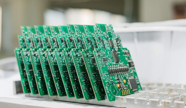
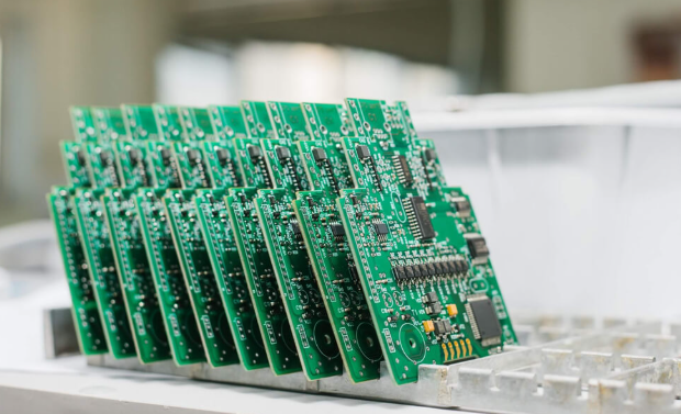
PCB assembly in Belarus is a critical link for local electronics manufacturers, ensuring the smooth operation of industrial equipment, medical devices, and aerospace components. We specialize in providing high-quality, reliable PCB assembly in Belarus, covering all stages from component sourcing to final delivery, to solve the core needs of local enterprises.

Are You Facing These Pain Points of PCB Assembly in Belarus?
- Do you struggle with unstable component supply for PCB assembly in Belarus, leading to production delays and project stagnation?
- Is it difficult to find a professional PCB assembly manufacturer in Belarus that can handle high-precision processes like BGA assembly?
- Are you worried about the lack of traceability in the production process, making it hard to locate quality problems in PCB assembly in Belarus?
- Do you face long lead times for PCB assembly in Belarus, failing to meet the urgent delivery needs of your projects?
- Is it challenging to find a PCB assembly company in Belarus that can provide customized solutions for medical or aerospace industry requirements?
- Do you encounter quality inconsistencies in PCB assembly in Belarus, resulting in high rework rates and wasted resources?
Our Targeted Solutions to Pain Points of Belarus PCB Assembly
We address each core pain point with specific actions embedded in our one stop workflow, ensuring predictable outcomes for your Belarus projects.
For unstable component supply, we leverage our global supplier network and safety stock of critical parts. Our dedicated purchasing team conducts rigorous incoming inspections to keep your PCB assembly in Belarus on track.
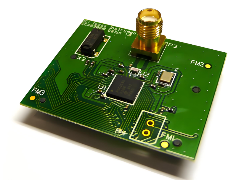
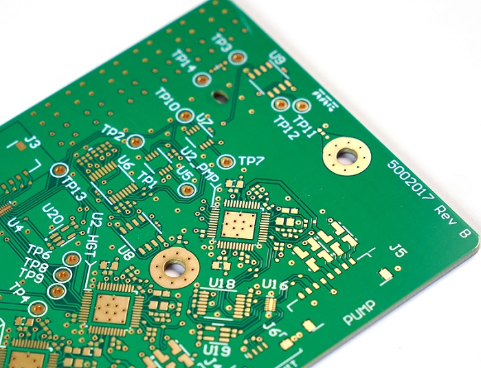
For high precision assembly needs, we deploy equipment capable of 01005 components and 0.25mm pitch BGA. Our engineering team specializes in complex layouts, ensuring consistent accuracy for your most demanding Belarus projects.
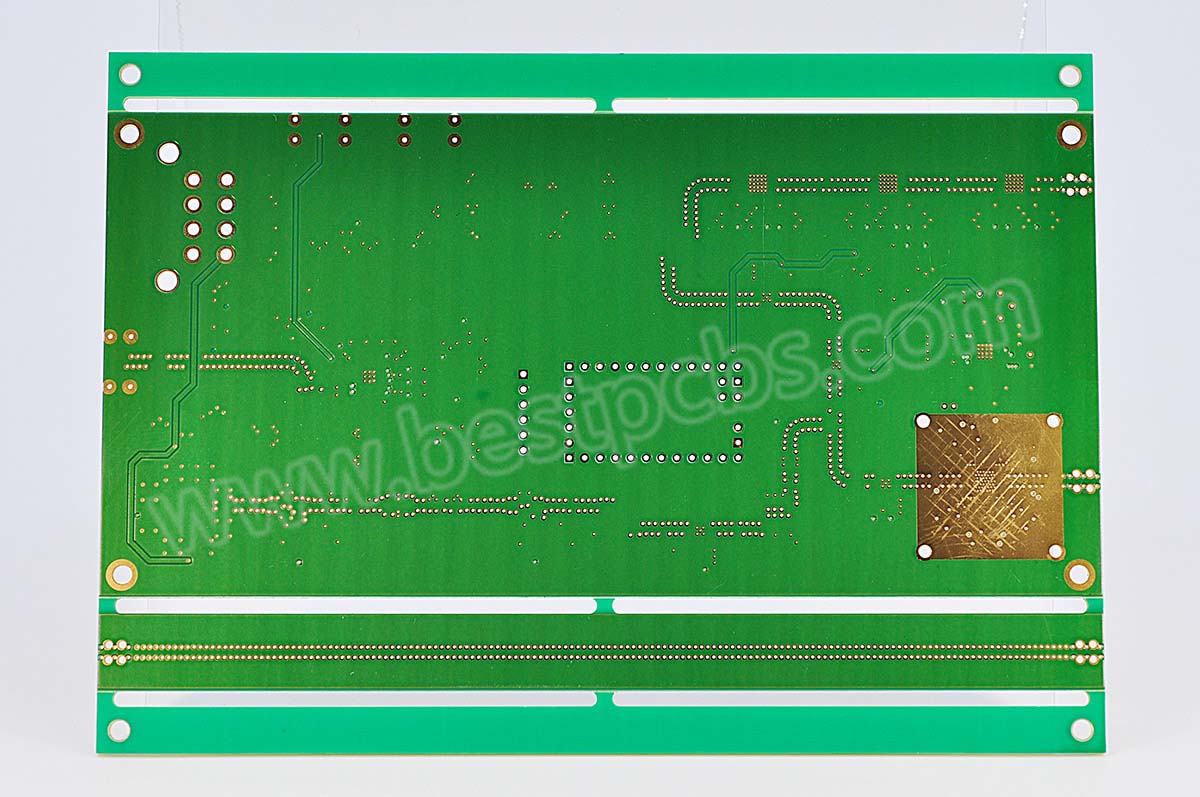
For missing traceability, our MES system logs every production step in real time. Component lot numbers, machine settings and inspection results are all recorded for rapid root cause analysis in PCB assembly in Belarus.
For long lead times, our agile scheduling and 24 hour expedite service keep projects on schedule. Standard orders for PCB assembly in Belarus ship in 1 to 5 days, with urgent orders prioritized at every stage.
For regulated industry compliance, we align our processes with ISO 13485 and AS9100D. We tailor material selection, assembly and testing to meet the strict requirements of medical and aerospace PCB assembly in Belarus.
For low yield from design flaws, our free pre production DFM analysis is non negotiable. We fix placement, thermal and solderability issues early, reducing rework and ensuring high first pass yield for PCB assembly in Belarus.
Why Choose EBest for PCB Assembly Company in Belarus?
Founded on June 28 2006, EBest Technology (Best Technology) brings over 19 years of proven expertise in delivering one stop PCB solutions designed to save you time money and resources. We are dedicated to driving technological advancement and innovation serving clients worldwide including those in Belarus with a focus on solving your unique PCB assembly challenges and helping you stay competitive in the local electronics market.
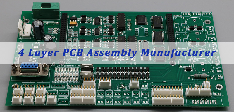
Our core advantage is our fully integrated one stop PCBA service which eliminates the hassle of coordinating multiple suppliers and reduces the risk of delays miscommunication and quality inconsistencies. We seamlessly integrate PCB fabrication component sourcing assembly testing and delivery into a single streamlined process ensuring consistent quality efficient turnaround and cost savings for your PCB assembly in Belarus. This end to end service lets you focus on your core business while we handle every detail of your PCB assembly needs.
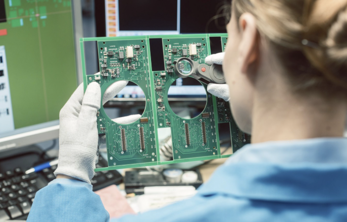
We adopt a state of the art MES system to achieve full process traceability a critical benefit for your compliance and quality assurance. Every step from component incoming to final assembly is recorded in real time allowing us to quickly locate and resolve any quality issues before they impact your projects. This traceability not only ensures the reliability of your PCB assembly in Belarus but also simplifies regulatory compliance for medical aerospace and industrial applications.
We offer free DFM design for manufacturability analysis a valuable service that helps you avoid costly rework delays and design flaws. Our experienced engineering team reviews your PCB design to identify potential manufacturing issues in advance optimizing the design to improve yield reduce production costs and accelerate time to market. This proactive approach is crucial for high precision PCB assembly in Belarus and ensures your projects stay on budget and on schedule.
We prioritize fast and reliable lead times to keep your operations running smoothly. Our standard lead time for PCB assembly in Belarus is 1 to 5 days and we offer a 24 hour expedite service for urgent orders ensuring urgent boards can be shipped out within 24 hours to meet your tight project schedules. Additionally we maintain a strategic inventory of commonly used components to further reduce lead times and prevent production delays caused by component shortages.
Beyond these core advantages, we also offer personalized support with a dedicated account manager for your projects, so you can get help whenever you need it. We understand your industry needs and guarantee reliable, compliant results. We also provide flexible order options, whether you need small batches for your research or large volumes for full production, to support your business growth seamlessly.
What Types of PCB Assembly Service in Belarus Can We Provide?
We offer tailored PCB assembly services in Belarus to meet the unique needs of medical, aerospace and industrial equipment sectors, covering standard, high-precision and customized requirements.
Our core services include BGA assembly, through-hole assembly and flex PCB assembly, each designed to fit specific PCB types and application needs for your projects.
We provide ceramic PCB assembly for high-temperature, high-frequency use cases, prototype PCB assembly to support your R&D efforts, and quick turn PCB assembly to meet your urgent order deadlines in Belarus.
Our full turnkey PCB assembly service handles every step from component sourcing to final delivery, freeing you from supplier coordination and ensuring a seamless, hassle-free experience for your PCB assembly needs.
Our core assembly services include BGA assembly service, through-hole assembly, and flex PCB assembly, suitable for different PCB types and application scenarios.
We also offer ceramic PCB assembly for high-temperature, high-frequency applications, prototype PCB assembly for R&D projects, and Quick Turn PCB Assembly for urgent orders in Belarus.
In addition, our full turnkey PCB Assembly service covers all aspects from component sourcing to final delivery, providing a hassle-free solution for your PCB assembly needs in Belarus.
Our PCB Assembly Capabilities for Belarus PCBA Orders
| Parameter | Value |
| Placer Speed | 13,200,000 chips/day |
| Bare Board Size | 0.2″ × 0.2″ – 20″ × 20″ / 22″ × 47.5″ |
| Minimum SMD Component | 01005 |
| Minimum BGA Pitch | 0.25mm |
| Maximum Component Size | 50mm × 150mm |
| Assembly Type | SMT, THT, Mixed Assembly |
| Component Packaging Types | Reels, Cut Tape, Tube, Tray, Loose Parts |
| Standard Lead Time | 1 – 5 days |
| Expedite Service Lead Time | Within 24 hours |
How Can We Ensure the Reliability of PCB Assembly in Belarus?
Methods about we ensure the quality and reliability of PCB assembly in Belarus:
- We hold authoritative certifications including IATF 16949, ISO 9001:2015, ISO 13485:2016, and AS9100D. These globally recognized standards guarantee our PCB assembly in Belarus fully meets the strict quality requirements of medical, automotive, and aerospace industries, helping you avoid compliance risks and build customer trust.
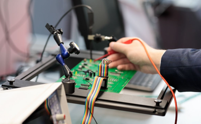
- We perform 100% pre-delivery inspection on every PCB assembly in Belarus, using advanced AOI visual detection and X-ray testing to eliminate defective products. This ensures your PCBs arrive ready for immediate integration into your production line, saving you time on additional inspections and reducing costly rework.
- We exclusively use top-grade materials for all PCB assembly orders in Belarus and maintain a stable, globally vetted component supply chain. Our strict incoming material inspections, including a dedicated “golden sample” comparison process, ensure consistent quality across every batch, preventing disruptions to your operations.
- Our free pre-production DFM analysis is a proactive service that catches design flaws early. By optimizing your PCB design before assembly, we reduce rework costs, improve production yield, and keep your PCB assembly in Belarus on schedule, accelerating your time to market.
- Our state-of-the-art MES system tracks every production step of your PCB assembly in Belarus in real time, from component incoming to final inspection. This full traceability allows us to quickly identify and resolve any quality issues, minimizing delays and ensuring reliable finished products.
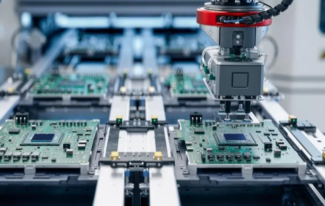
- We maintain industry-leading automated production lines with regular equipment calibration and lean management practices. This ensures consistent placement accuracy and process stability, keeping product defect rates at a minimum and delivering reliable PCB assembly in Belarus.
- Our experienced engineering team provides ongoing quality oversight, with dedicated specialists assigned to monitor critical assembly processes. This hands-on approach ensures any potential issues are addressed promptly, safeguarding the quality and reliability of your PCB assembly orders in Belarus.
How Can We Ensure the On-Time Delivery of Belarus PCBA Orders?
Methods about we ensure the on-time delivery of PCB assembly in Belarus:
- One-stop full-process services covering PCB prototyping, component procurement, SMT/THT assembly, functional testing, and finished product delivery, eliminating the need for multi-vendor coordination and reducing management effort and communication costs by over 50%. Supports R&D small-batch samples to mass production, accommodating orders from 10 sets to tens of thousands, with flexible production lines balancing adaptability and efficiency.
- High-precision assembly capabilities handling 01005-sized ultra-small SMD components and minimum BGA pitch of 0.25mm. Equipped with high-speed precision placement machines (daily capacity 13.2 million chips), meeting high-density, high-reliability demands for medical and aerospace sectors. Full-process quality control via AOI optical inspection, X-Ray inspection, and other advanced equipment, with first-pass yield consistently above 99.8% and solder joint quality compliant with IPC Class 3 standards.
- Stable global supply chain and rapid delivery through long-term partnerships with mainstream component manufacturers and stocked common components, preventing material shortages. Standard lead time 1-5 days, with 24-hour expedited service available, achieving 99% on-time delivery accuracy to meet Belarus local and urgent project needs.
- Free DFM (Design for Manufacturing) analysis by professional engineers to identify PCB design flaws early, optimize component layout and pad design, improving yield by 10-15% on average and reducing rework costs and R&D cycles. Customized solutions with certifications like ISO 13485 and AS9100D for regulated industries such as medical and aerospace.
- Full-process traceability and multi-level quality control using MES systems to record component sourcing, production, testing, and shipping in real time for quick issue tracing. Triple inspections from raw materials to finished goods, using only Grade A components, with 100% full inspection of each batch to ensure consistency.
- Comprehensive compliance certifications including IATF 16949 (automotive), ISO 9001:2015 (general), ISO 13485:2016 (medical), and AS9100D (aerospace), covering Belarus’s key electronics manufacturing sectors to mitigate compliance risks. Dedicated account managers provide 24/7 response, real-time order updates, and one-on-one technical and delivery support.
- Cost-effective and transparent pricing leveraging scaled production and bulk procurement advantages, with costs 28% lower than European and US manufacturers while maintaining quality. Clear quotes with no hidden fees, supporting on-demand procurement and lean inventory management to reduce capital occupancy and improve turnover efficiency.
Case Studies: Medical PCB Assembly in Belarus
Project Background: A leading medical device manufacturer in Belarus needed PCB assembly for a portable blood glucose monitor. The device requires high precision and reliability to ensure accurate blood glucose readings, complying with ISO 13485:2016 standards.
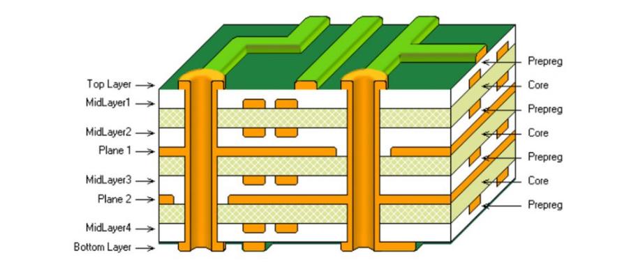
Project Requirements: The PCB required BGA assembly with a minimum pitch of 0.3mm, 8-layer FR4 substrate, and integration of SMD components (01005 size). The lead time was 3 days, and the yield rate needed to be no less than 99.5%.
Project Difficulties: The 0.3mm BGA pitch required high-precision assembly to avoid short circuits. The compact design of the medical device also demanded strict control of PCB size and component placement, with no room for error. Additionally, the tight 3-day lead time left no room for rework, requiring flawless first-pass assembly.
Our Solutions
- We first conducted free DFM analysis to optimize the PCB design, adjusting component placement to improve assembly accessibility and reduce short-circuit risks.
- We used high-precision placement equipment (13,200,000 chips/day speed) for BGA assembly, followed by X-ray inspection to ensure solder joint quality.
- We prioritized the order in our production schedule, assigning a dedicated team to monitor each process, and used expedited logistics to meet the 3-day lead time.
Output Results
We delivered 500 PCBs within 3 days, achieving a yield rate of 99.8%, exceeding the client’s requirement of 99.5%. All PCBs passed ISO 13485:2016 inspection, with zero defective products.
The client integrated the PCBs into their blood glucose monitors, which achieved a 99.9% accuracy rate in clinical tests. We have since become their long-term PCB assembly partner in Belarus, supporting their subsequent product upgrades.
FAQs About PCB Assembly in Belarus
Q1: What types of PCB assembly services do you offer for medical devices in Belarus?
A1: We provide specialized PCB assembly services for medical devices in Belarus including BGA assembly flexible PCB assembly and ceramic PCB assembly. All services comply with ISO 13485 2016 standards with strict quality control and traceability to ensure device reliability. We also offer free DFM analysis to optimize designs for medical applications.
Q2: Can you provide expedited PCB assembly service in Belarus for urgent orders?
A2: Yes we offer expedited PCB assembly service in Belarus. Urgent orders can be shipped within 24 hours with no compromise on quality. Our high speed placement equipment and flexible production scheduling enable us to meet tight deadlines for your urgent projects.
Q3: How do you ensure component quality for PCB assembly in Belarus?
A3: We source components from trusted suppliers and conduct strict incoming inspections. Our stable supply chain covers all electronic components and we verify each component’s quality before assembly. We also provide component traceability through our MES system to ensure reliability.
Q4: Is DFM analysis included for PCB assembly orders in Belarus?
A4: Yes we provide free DFM analysis for all PCB assembly orders in Belarus. Our team reviews your design to identify potential manufacturing issues and optimizes it to improve yield reduce rework and lower production risks. This proactive service helps keep your projects on track and within budget.
Q5: What is the standard lead time for PCB assembly in Belarus?
A5: Our standard lead time for PCB assembly in Belarus is 1 to 5 days depending on order size and complexity. For small batch prototype orders we can deliver within 1 to 2 days while large batch orders have a lead time of 3 to 5 days. We also provide real time progress tracking to keep you informed.