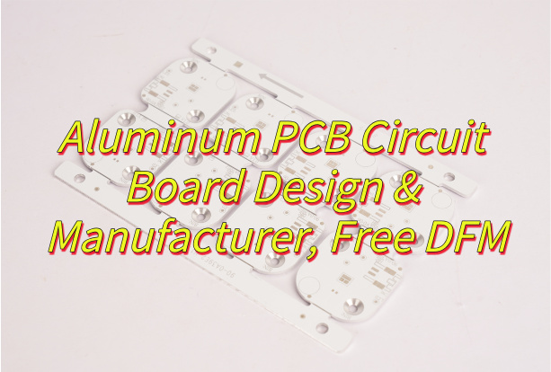
Bluetooth module PCB is the heart of any wireless connectivity solution. Whether it’s for audio streaming, smart devices, or industrial controls, this PCB powers reliable communication.
EBest Circuit (Best Technology) produces trustworthy Bluetooth module PCB from prototype to assembly services in a highly competitive market. We have gained some valuable experience within the medical, consumer electronics, and automotive industries from our 19 years of seniority. We are able to give you some practical solutions according to your specific project needs. No matter what the PCB material should be used, or which PCB type is workable, or how to optimize the Bluetooth module PCB layout, EBest Circuit (Best Technology) delivers available customization for your Bluetooth module PCB. If you need the particular quote, please email us at sales@bestpcbs.com or call us at +86-755-2909-1601. We will try our best to satisfy you.
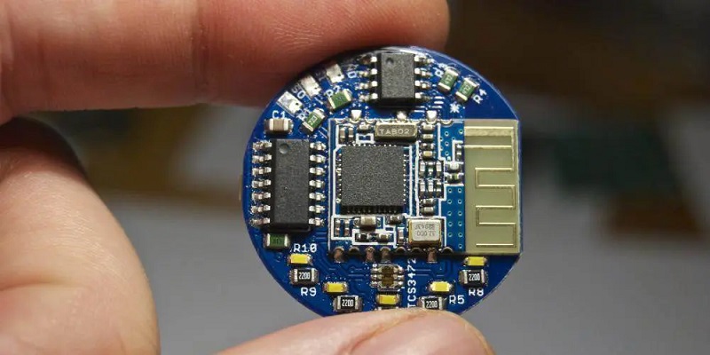
What Does a Bluetooth Module PCB Do?
A Bluetooth module PCB provides short-range wireless communication between devices. It manages radio frequency signals, handles signal encoding, and integrates with microcontrollers or processors. It ensures a smooth data exchange without cables, enabling features like wireless audio, data sync, and device pairing.

What is the Difference Between Wi-Fi PCB and Bluetooth Module PCB?
Though both use radio waves, their roles differ. A Wi-Fi PCB targets high-speed data for internet access, while a Bluetooth module PCB focuses on low-power, close-range device-to-device communication. Wi-Fi PCBs are heavier on bandwidth; Bluetooth PCBs excel in power saving and are simpler to integrate for mobile and wearable devices.
What Are the Different Types of Bluetooth PCB Modules?
There are several kinds:
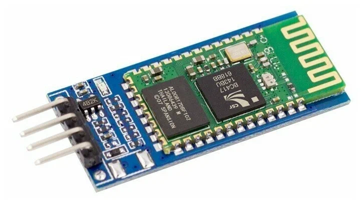
- Bluetooth Classic Modules – Ideal for higher data transfer (e.g., Bluetooth module HC-05).
- Bluetooth Low Energy (BLE) Modules – For low-power needs like fitness trackers.
- Audio Receiver Modules – For Bluetooth speakers or headphones.
- Embedded System Modules – Fully integrated microcontrollers and Bluetooth on one board.
What Is the Purpose of a Bluetooth Audio PCB Module?
This type enables wireless sound streaming. You’ll find them in headsets, portable speakers, car kits, and more. They handle audio data encoding, transmission, and sometimes even amplify the sound. Bluetooth audio PCB modules often support stereo output and offer decent range with minimal interference.
What Is the Bluetooth Module PCB Price?
The Bluetooth module PCB price varies based on:
1. Complexity
- Basic modules (e.g., BLE-only) may cost less in bulk orders
- Advanced modules (e.g., dual-mode Bluetooth audio) require multilayer FR4 boards and RF shielding, increasing costs
2. Materials
- some special material and testing expenses will impact the costs
- Custom layouts for specific antenna designs or form factors add NRE (non-recurring engineering) fees
3. Production Scale
- Mass production (e.g., 10k+ units) enables batch optimization and cost reduction
- Small-volume orders prioritize quick-turn fabrication, raising per-unit prices
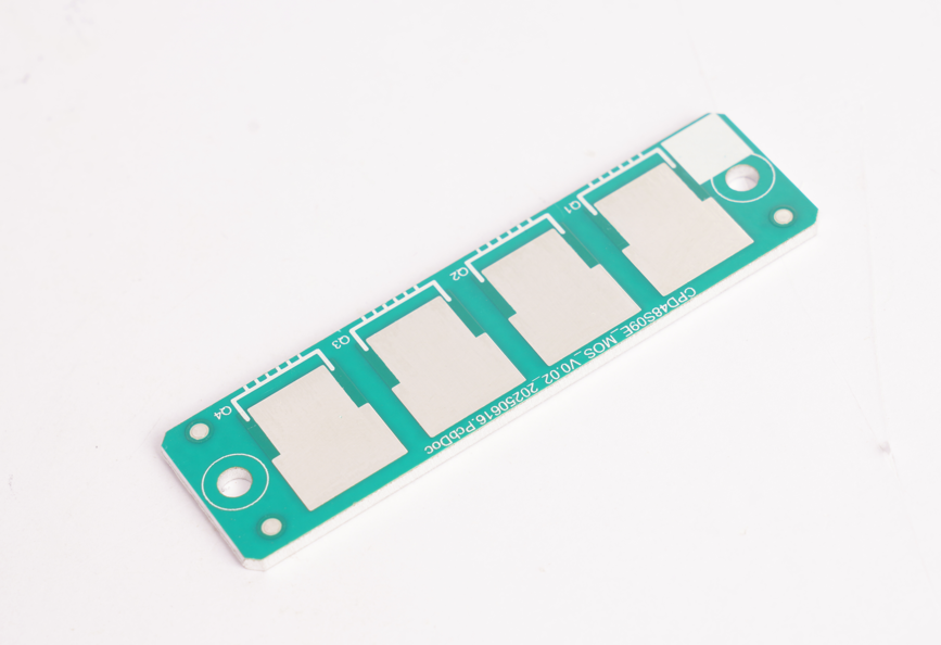
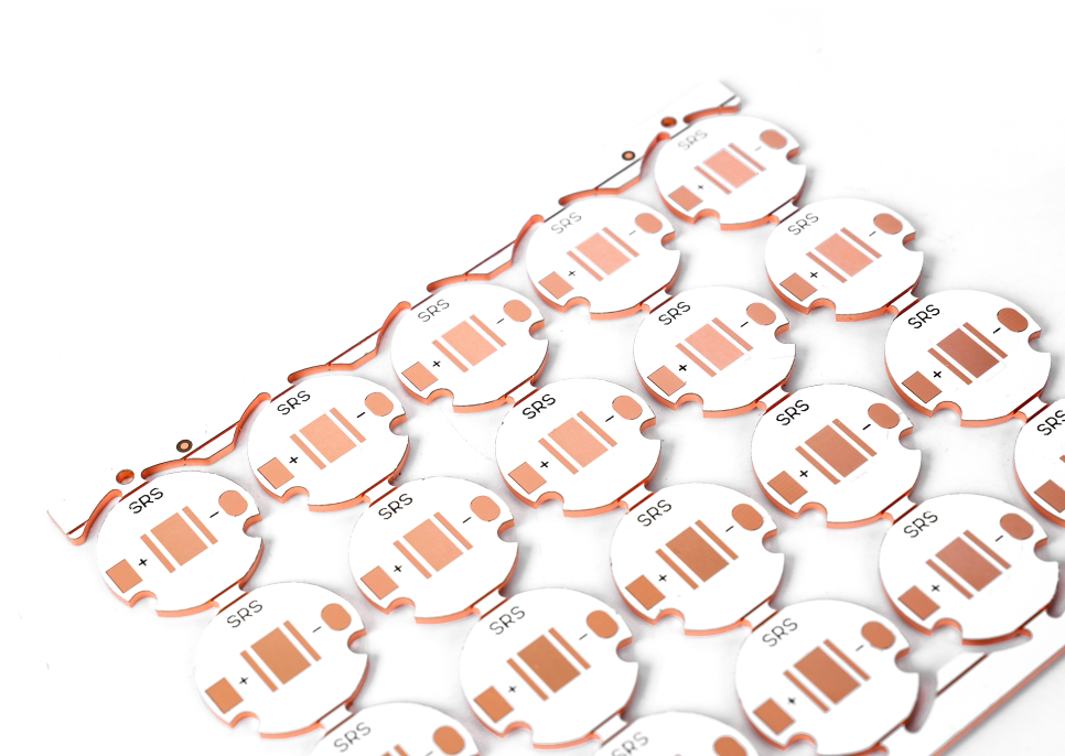
What Is the Manufacturing Process of Bluetooth Module HC-05 PCB?
The process involves:
- PCB layout & design: With focus on impedance control and antenna placement.
- Material selection: FR-4 or Rogers depending on signal needs.
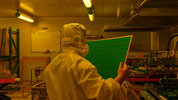
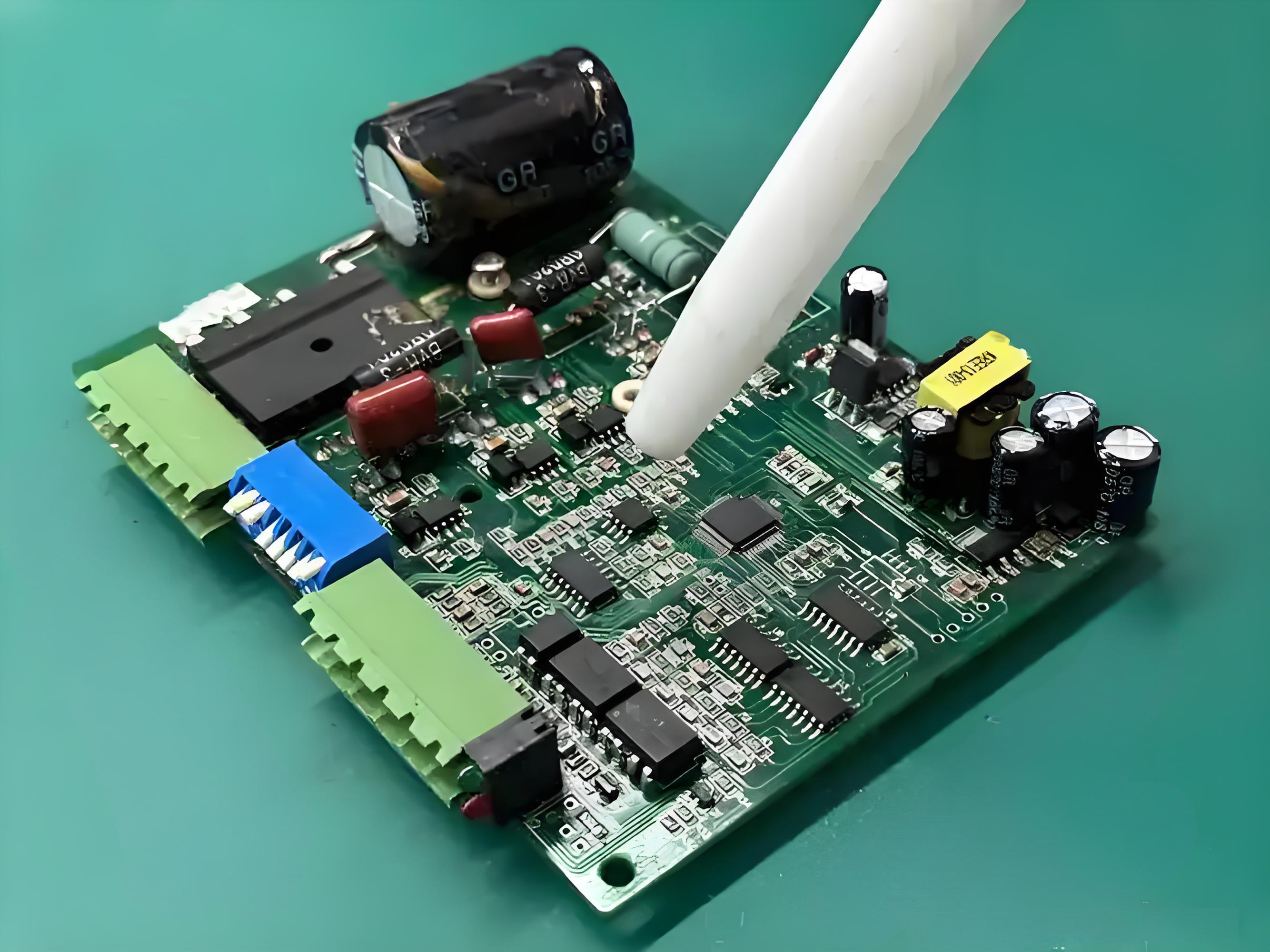
- Fabrication: Multilayer etching, HASL lead-free coating, soldermask printing.
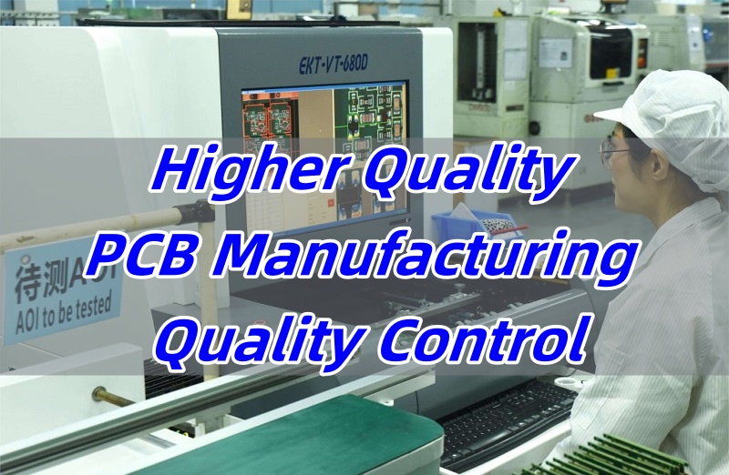
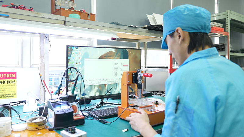
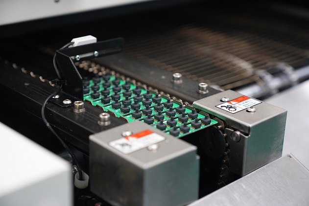
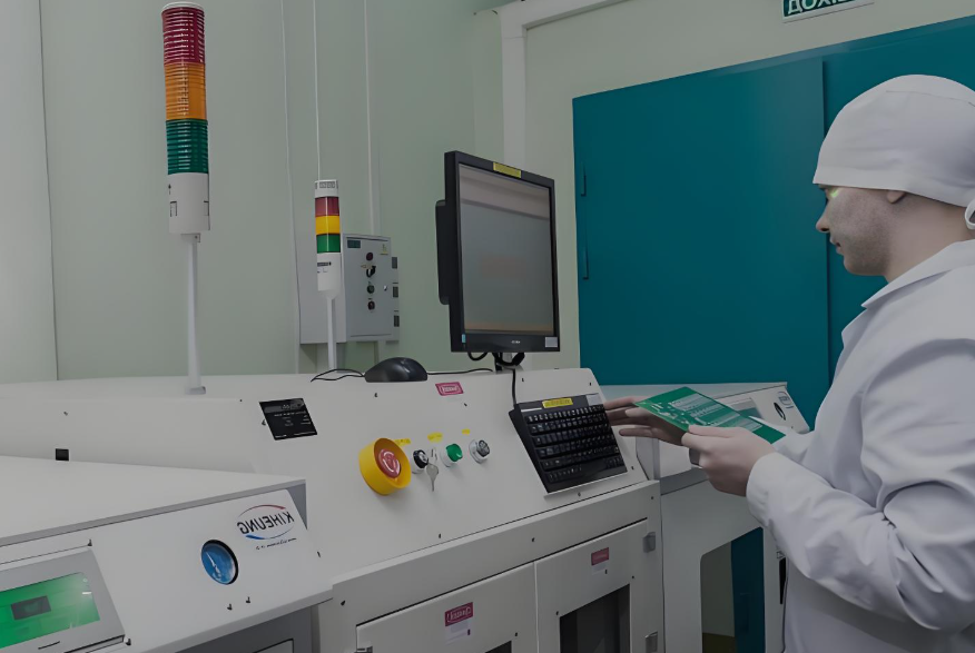
- Assembly: Component placement with SPI + AOI inspection.
- Firmware preloading: Including manufacturing test codes.
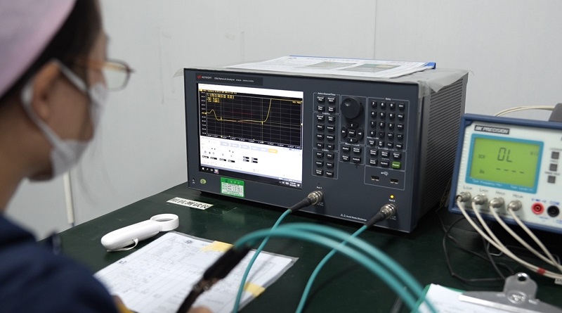
- RF testing: Using sophisticated inspection equipment to measure power, BER, and range.
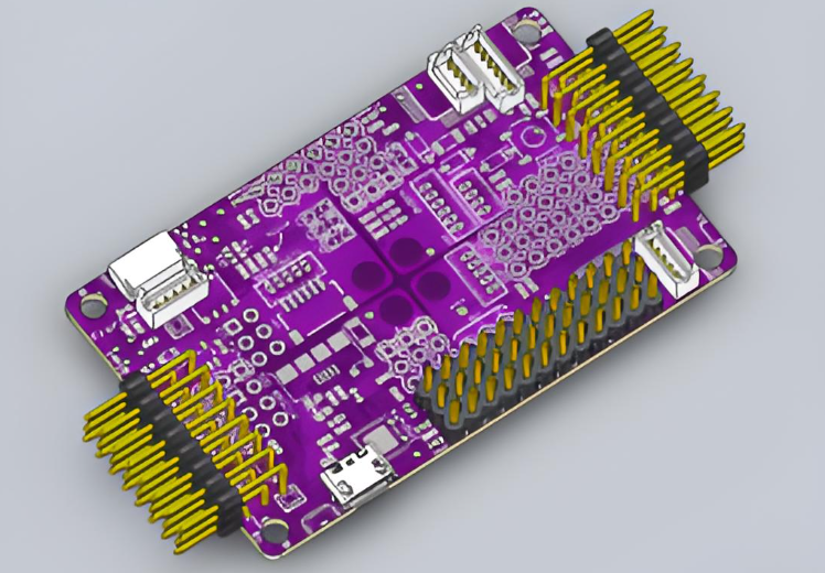
How to Ensure Quality of Rigid-Flex PCB for Bluetooth Module Circuit Board?
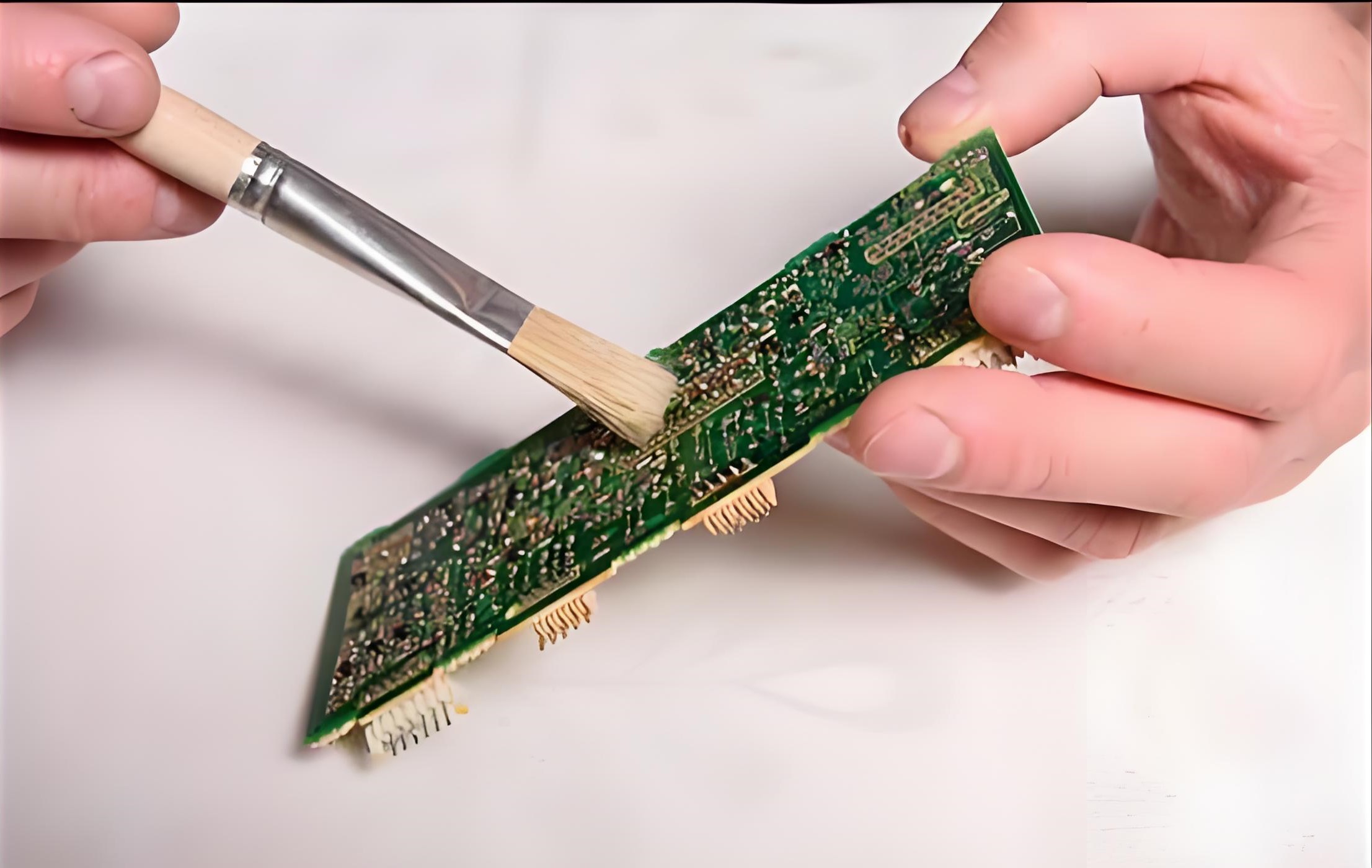
Rigid-flex PCBs are essential for wearables and compact modules. EBest Circuit (Best Technology) addresses defects by using controlled impedance routing and enhanced grounding. We add stitched vias every 100 mils to reduce heat buildup and EMI. All PCBs go through 3D solder paste inspection and ESD-safe assembly lines, ensuring consistent quality even at scale.
What Is the Application of Bluetooth Module PCB?
These PCBs are everywhere:
- Smartphones & tablets
- Wearable devices
- Industrial automation
- Wireless audio systems
- IoT gateways and sensors
- Bluetooth-enabled tools or kits
They’re also used in automotive applications and medical devices. Reliability and RF clarity are critical in such fields.
Why Choose EBest Circuit (Best Technology) for Manufacturing China Bluetooth Module PCB?
Workable PCB solutions: 92% of engineers face RF interference. Our engineers fix that with smart antenna layout, GFSK modulation, and grounding strategies.
24/7 Technical Support: 75% of prototype failures stem from design flaws. We prevent that with automated DFM checks, proper power routing, and controlled impedance. If you have any technical problems, you are welcome to call us at +86-755-2909-1601 anytime.
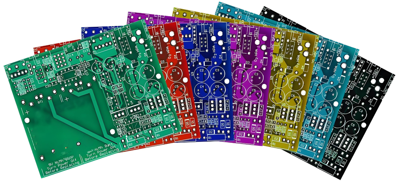
High Mix Bluetooth Module PCB: Our product line features a variety of PCB options, such as rigid PCB, flex PCB, rigid-flex PCB, ceramic PCB, MCPCB, and so on. We will recommend the corresponding type for your needs.
Fast Delivery: We have adopted both day shift and night shift in our PCB and PCBA workshop. And our lead time policy is 2-3 weeks to better suit our customers’ needs and expedite their market entry time. No matter how complex the Bluetooth PCB design, we will adhere to this policy consistently.
Full Turnkey Service: We provide material procurement, Bluetooth PCB prototype, fabrication, and assembly services. That eliminates a variety of troubles and saves your time and costs.
The Bluetooth module PCB isn’t just a circuit board—it’s a foundation for your entire wireless product. From prototype to final assembly, EBest Circuit (Best Technology) provides more than just fabrication. We offer engineering that eliminates RF risks, design flaws, and firmware issues.
Our expert team ensures traceability with MES systems, applies ISO 9001, ISO 13485, AS9100D standards, and delivers highly customized options like HASL lead-free surface, rigid-flex formats, and tailored soldermask. With faster response times and engineering consultation, we help reduce redesigns and speed up market entry. If you need to tailor the Bluetooth module PCB solutions, pls email your Gerber files to us at sales@bestpcbs.com. We are happy to give you the practical quote and the lead time you need.