If you’ve spotted a “5G UC” label in your smartphone’s status bar lately, you’re not alone in wondering what it means. Is it faster than regular 5G? Do you need a special plan to use it? And why does it sometimes disappear when you move a few feet? This guide breaks down everything you need to know about 5G Ultra Capacity (UC) — from its technical basics to real-world use cases, common frustrations, and how to make the most of it on your device.
What Does UC Mean Next to 5G?
Let’s start with the basics: “UC” stands for Ultra Capacity, a branding term coined by T-Mobile to describe its premium 5G network tier. Unlike standard “5G Extended Range” (T-Mobile’s low-band 5G), 5G UC combines mid-band (sub-6 GHz) and high-band (mmWave) frequencies to deliver faster speeds and more reliable connectivity for data-heavy tasks.
To put it simply: Regular 5G is great for basic browsing and social media, but 5G UC shines when you’re streaming 4K videos, gaming online, transferring large files, or video calling without lag. Think of it as a “highway” for your data — with more lanes to handle traffic, even during peak hours.
Key technical highlights of 5G UC:
- Combines mid-band (for balance of speed and coverage) and mmWave (for ultra-fast, short-range bursts)
- Average download speeds range from 89 Mbps to 418 Mbps (median 371 Mbps per RootMetrics)
- Covers 330 million people across all 50 U.S. states
- Requires a 5G-capable device and compatible plan (most modern plans include 5G UC access)
How 5G UC Compares to Other 5G Brands
You might have seen other 5G labels from competitors — here’s how 5G UC stacks up:
T-Mobile 5G UC vs. Verizon 5G UW vs. AT&T 5G+
| Feature | T-Mobile 5G UC | Verizon 5G UW (Ultra Wideband) | AT&T 5G+ |
|---|---|---|---|
| Focus | Mid + high-band | High-band (mmWave) | Mid + high-band |
| Coverage | 330M people (nationwide) | 100M+ people (urban focus) | 250M+ people |
| Avg Speed | 89-418 Mbps | 472 Mbps (theoretical peak) | 100-300 Mbps |
| Best For | Balanced speed + coverage | Urban 4K streaming/gaming | Business users + travelers |
The biggest advantage of 5G UC is its coverage — T-Mobile’s mid-band focus means you’ll get faster speeds in more places (including suburbs and small towns) compared to Verizon’s mmWave-only 5G UW.
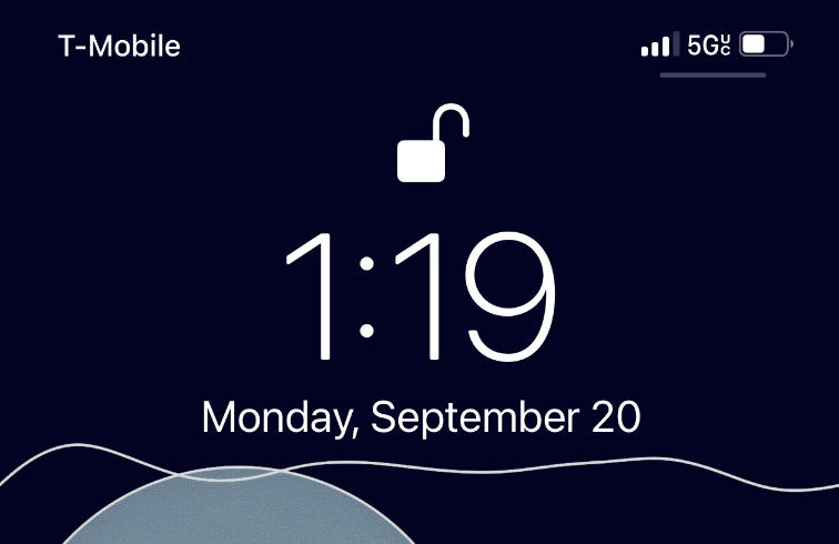
What Does 5G UC Mean on iPhone?
If you own an iPhone 12 or newer, you might have noticed the 5G UC icon popping up in certain areas. Here’s what it means for your Apple device:
Which iPhones Support 5G UC?
All iPhone models from the iPhone 12 series onward are compatible with 5G UC — as long as you’re on a T-Mobile (or MVNO using T-Mobile’s network) plan that includes 5G access. Older iPhones (iPhone 11 and below) don’t have 5G hardware, so they won’t display the 5G UC icon.
How to Enable 5G UC on Your iPhone
By default, iPhones optimize 5G usage for battery life, but you can adjust settings to prioritize 5G UC when available:
- Go to Settings > Cellular > Cellular Data Options
- Under “Voice & Data,” select “Enable 5G” (instead of “Auto 5G”)
- For maximum data usage (e.g., 4K streaming), choose “Data Mode > Allow More Data on 5G”
Note: Using “Enable 5G” full-time may reduce battery life slightly, as 5G radios use more power than LTE.
Why 5G UC Disappears on Your iPhone
Many iPhone users report the 5G UC icon vanishing when moving between rooms or locations — this is normal. 5G UC relies on mid-band/mmWave signals, which are more sensitive to obstacles like walls, buildings, and distance from towers. When your iPhone can’t maintain a strong enough 5G UC connection, it switches to regular 5G or LTE to keep you connected.
Real-World Benefits of 5G UC
What can you actually do with 5G UC that you couldn’t do with 4G or standard 5G? Here are the most impactful use cases:
Streaming & Entertainment
- Stream 4K movies/shows on Netflix, Hulu, or Disney+ without buffering
- Download a 2-hour HD movie in under 5 minutes (vs. 15+ minutes on 4G)
- Enjoy lag-free live sports streaming on the go
Gaming & Productivity
- Play online games (e.g., Fortnite, Call of Duty) with sub-20ms latency
- Transfer large work files (1GB+) in seconds instead of minutes
- Video conference on Zoom/Teams with crystal-clear HD quality, even in busy areas
Emergencies & Connectivity
- T-Mobile’s 5G UC network integrates with satellite services (T-Satellite) for emergency calls in remote areas
- More reliable connectivity during natural disasters when other networks may be congested
Common 5G UC Pain Points (and How to Fix Them)
Based on Reddit and user reports, 5G UC isn’t without frustrations. Here are the top issues and solutions:
Random Switching Between 5G UC and 4G
Many users complain about frequent network fluctuations between 5G UC and LTE. Fixes:
- Move closer to a window or open area to improve signal strength
- Disable “Adaptive Connectivity” in your phone’s settings (Pixel/Android)
- Reset network settings: Settings > General > Transfer or Reset iPhone > Reset > Reset Network Settings
Dropped Calls on 5G UC
VoIP calls (RingCentral, Teams) and regular calls sometimes drop when connected to 5G UC. Solutions:
- Switch to “Auto 5G” mode (lets your phone use LTE for calls if 5G is unstable)
- Update your phone’s software (carriers often fix call issues via updates)
- Contact T-Mobile support to check for tower outages in your area
Slow Speeds Even With 5G UC Icon
If you see 5G UC but speeds are slow, try these steps:
- Check for network congestion (peak hours 7-11 PM often have slower speeds)
- Restart your phone to refresh the network connection
- Verify your plan includes 5G UC (some budget plans limit access to standard 5G)
5G UC Availability: Where Can You Get It?
5G UC is primarily a T-Mobile 5G UC network feature, but it’s also available on MVNOs (Mobile Virtual Network Operators) that use T-Mobile’s towers, such as:
- Mint Mobile
- Metro by T-Mobile
- Google Fi (when on T-Mobile towers)
- Cricket Wireless (select plans)
Coverage is strongest in major cities (New York, Los Angeles, Chicago) but expanding rapidly to rural areas. Use T-Mobile’s coverage map to check if 5G UC is available in your neighborhood.
FAQs About 5G UC
1. Do I need a new plan for 5G UC?
No — most T-Mobile plans (Magenta, Magenta Max, Essentials) include 5G UC access at no extra cost.
2. Is 5G UC better than 4G LTE?
For data-heavy tasks, yes — 5G UC is 5-20x faster than LTE. For basic calls/texts, LTE is still reliable.
3. Can Android phones use 5G UC?
Yes — most Android phones from 2020 onward (Samsung Galaxy S20+, Pixel 5+, OnePlus 8T+) support 5G UC.
4. Why doesn’t my phone show 5G UC?
Possible reasons: Your phone isn’t 5G-compatible, you’re outside T-Mobile’s 5G UC coverage area, or your plan doesn’t include 5G access.
5. Does 5G UC use more data?
It can — faster speeds make it easier to stream HD content or download large files, which uses more data. Enable “Low Data Mode” if you have a limited plan.
6. Is 5G UC available internationally?
No — 5G UC is a T-Mobile-specific brand. Other countries have their own 5G tiers (e.g., 5G+ in Europe, 5G Pro in Asia).
7. Will 5G UC replace 4G?
Not anytime soon — 4G LTE will remain the backbone of mobile networks for years, especially in rural areas where 5G coverage is limited.
How to Test 5G UC Speeds
Want to see if 5G UC is living up to its speed claims? Here’s how to test it:
- Download the Ookla Speedtest app (recommended by carriers)
- Ensure your phone is connected to 5G UC (check the status bar)
- Run 3-5 tests in different locations (indoors, outdoors, near windows)
- Compare results to T-Mobile’s average speeds (89-418 Mbps)
If your speeds are consistently below 50 Mbps, contact T-Mobile to troubleshoot — you may need a new SIM card or have a device compatibility issue.
Future of 5G UC: What’s Next?
T-Mobile is continuing to expand 5G UC coverage and upgrade its network with 5G Advanced (5.5G), which integrates AI to deliver even faster speeds (up to 10 Gbps) and lower latency. Future improvements will include:
- Better indoor coverage (reducing icon fluctuations)
- Enhanced voice call quality on 5G (VoNR)
- Support for new devices like foldables and smartwatches
As 5G Advanced rolls out, 5G UC will remain the base tier for premium 5G, with 5G Advanced as the next step up for power users.
Conclusion: Making the Most of 5G UC
5G Ultra Capacity is more than just a label — it’s a significant upgrade over standard 5G, offering faster speeds and better performance for the apps and tasks you use daily. Whether you’re streaming, gaming, or working on the go, understanding how to enable and optimize 5G UC on your device (especially iPhones) will help you get the most out of your mobile plan.
If you’re still having issues with 5G UC (e.g., constant drops, slow speeds), start with the troubleshooting steps above or reach out to your carrier. With coverage expanding and network upgrades ongoing, 5G UC is only going to get better in the coming years.