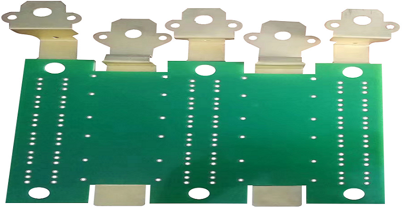
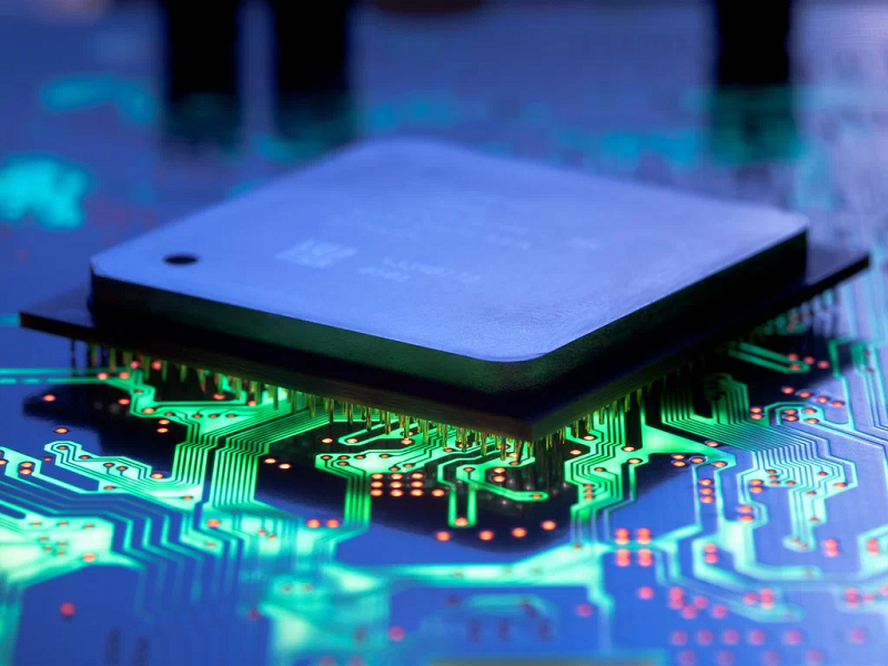
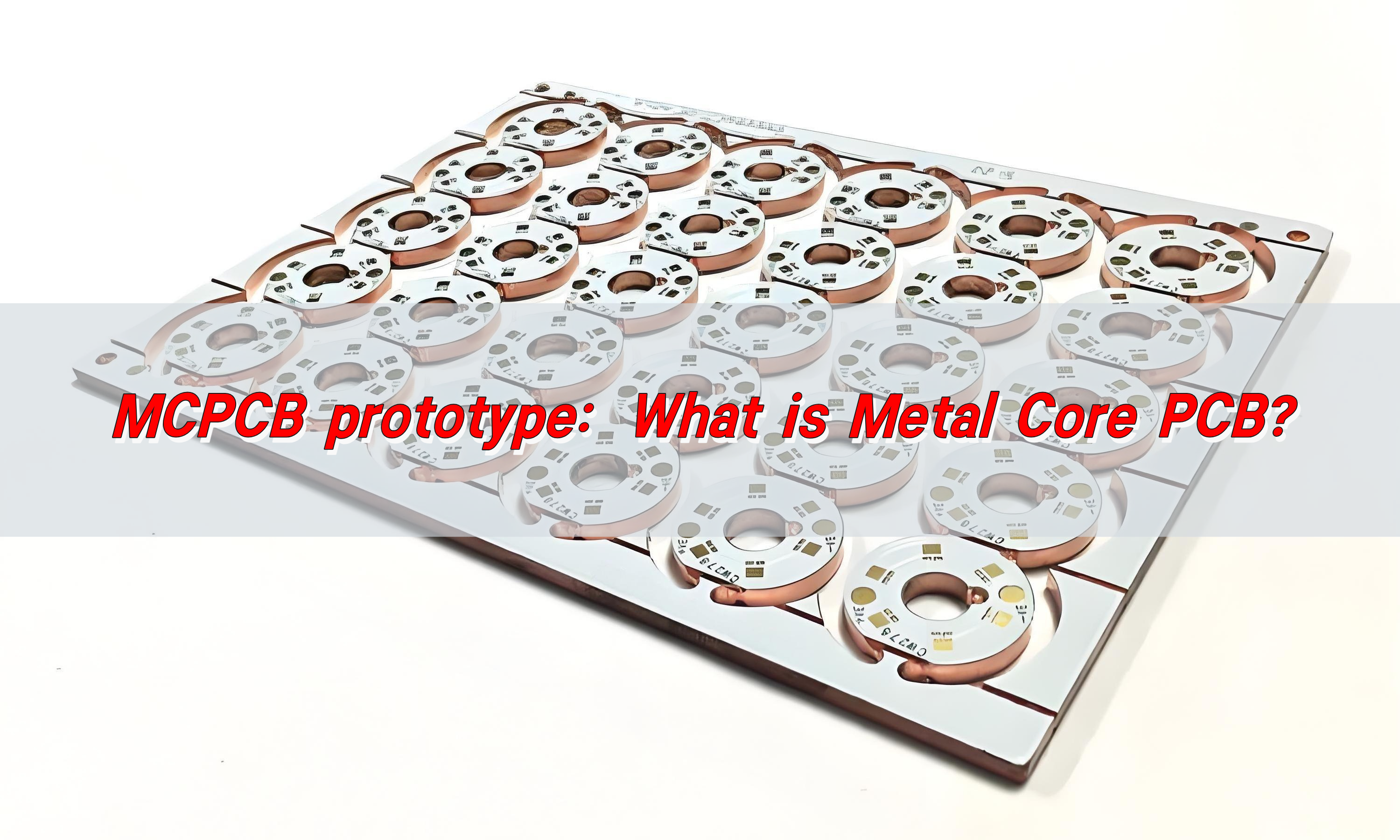
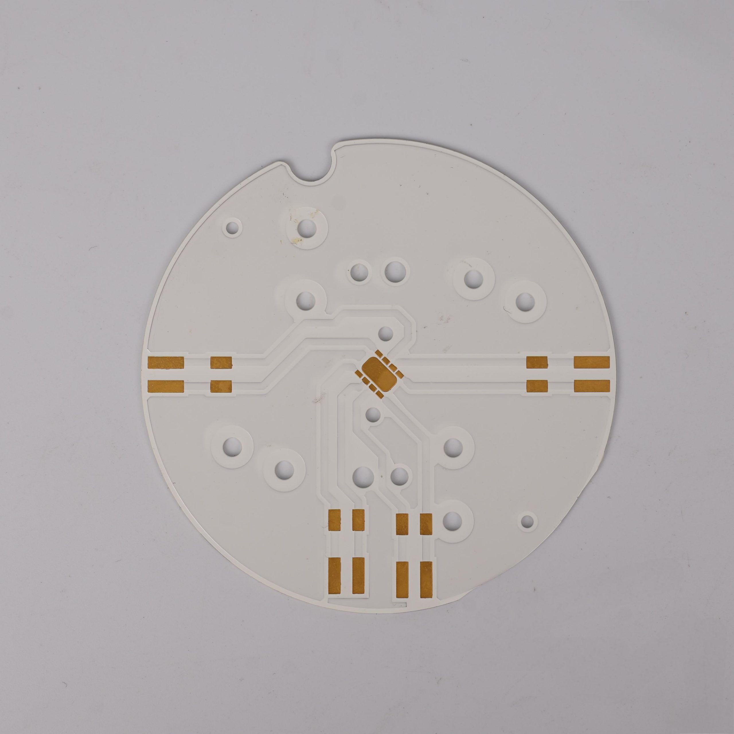
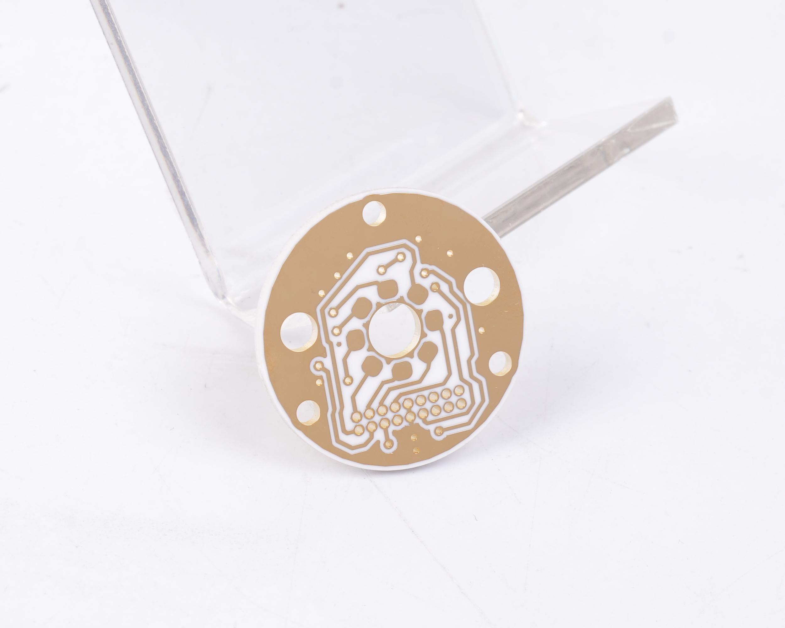
Round shape ceramic PCB is a special circuit board with ceramic material as substrate. It has high thermal conductivity, excellent electrical insulation and good mechanical strength. It is often used in electronic equipment with high frequency, high power and harsh environment. Its circular design is suitable for compact space and specific application scenarios, such as medical equipment, aerospace and wearable devices.
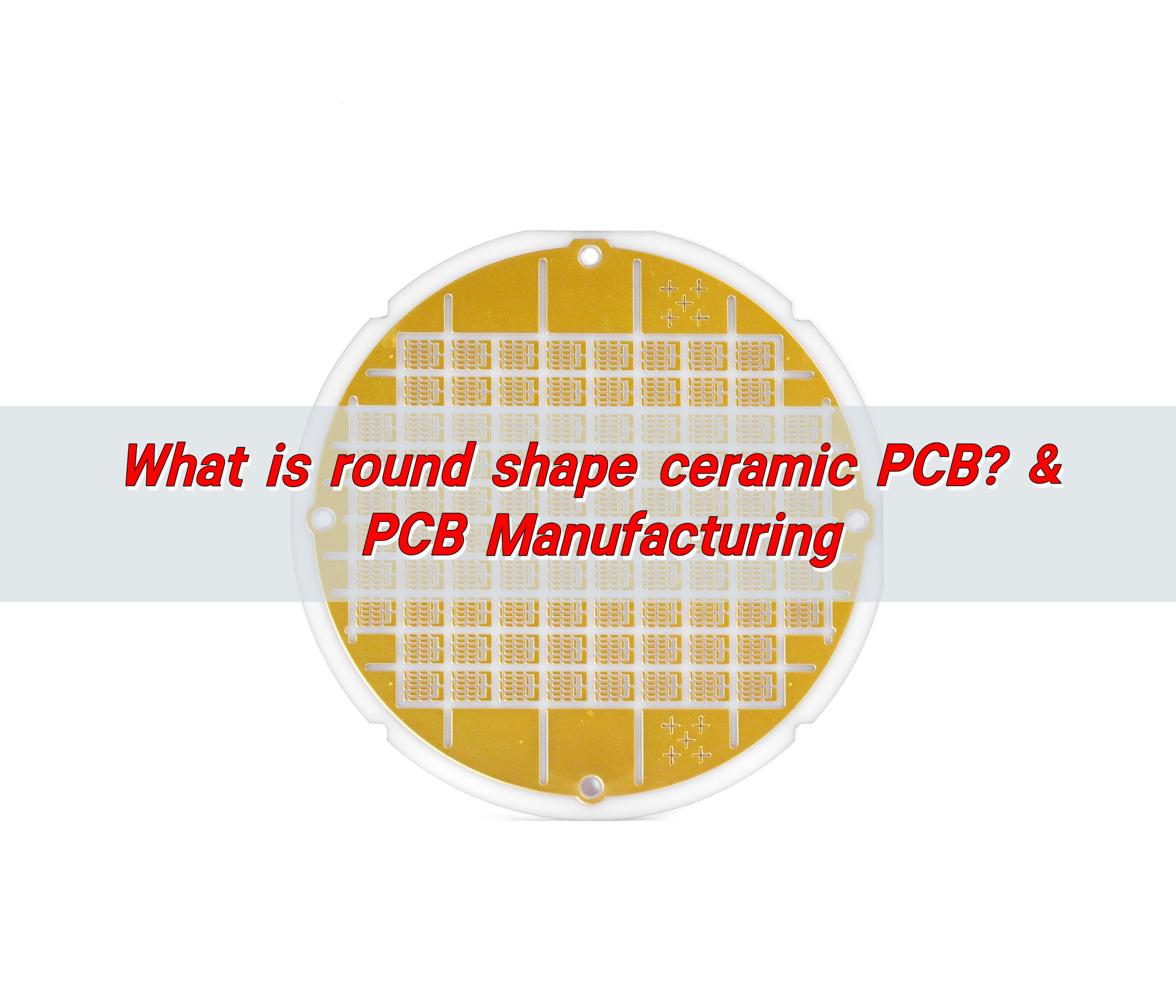
What is round shape ceramic PCB?
Round shape ceramic PCBs are specialized printed circuit boards (PCBs) that utilize ceramic materials as their base, with a distinctive round shape. These PCBs are used primarily in high-performance electronics that require superior thermal management, electrical properties, and stability.
Unlike traditional PCBs, which typically use fiberglass or other composite materials, ceramic PCBs are often employed in industries where heat dissipation and long-term reliability are crucial, such as automotive, aerospace, medical devices, and LED applications.
The round shape adds flexibility in design, particularly for devices that require circular or compact components, like LED lighting or certain high-frequency semiconductor applications.
How are round shape ceramic PCBs manufactured?
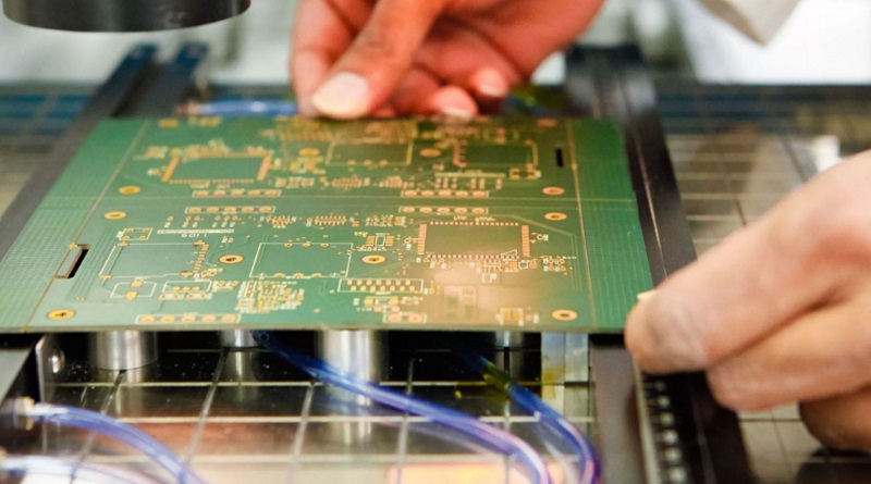
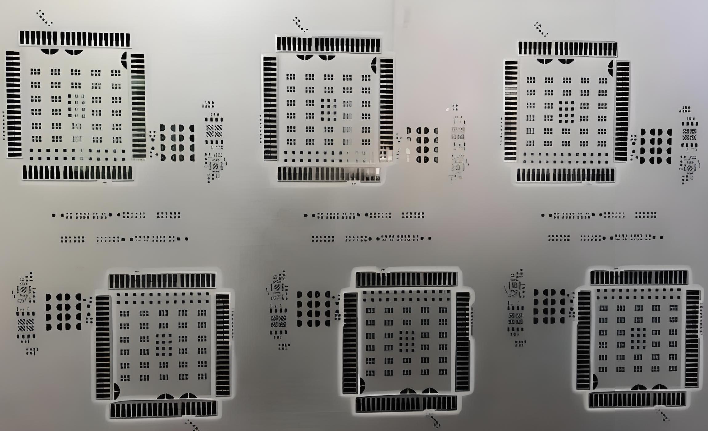
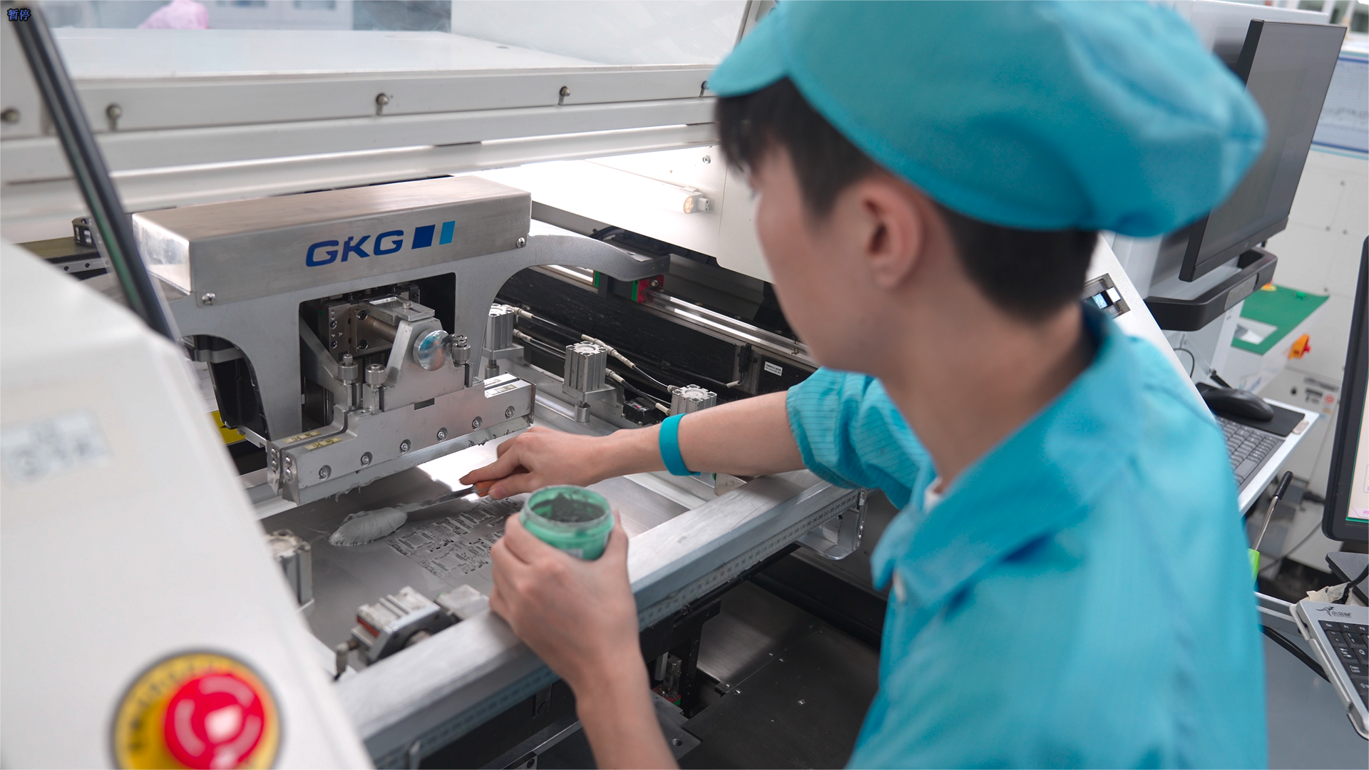
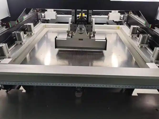
The manufacturing process for round shape ceramic PCBs is quite similar to traditional PCBs, with some added complexity due to the ceramic material used.
The first step involves selecting the right type of ceramic material, such as alumina (Al2O3), aluminum nitride (AlN), or zirconia (ZrO2), depending on the requirements for electrical insulation, heat dissipation, and mechanical strength. These ceramics are then shaped into round substrates, often using a cutting or grinding process to achieve the desired diameter.
Next, the ceramic base is coated with a conductive layer, typically copper, which is applied through a process called sputtering or electroplating. Once the conductive layer is added, the circuit pattern is etched onto the copper using a photolithography process.
This process involves applying a photosensitive layer, exposing it to light through a mask, and then chemically removing the unwanted copper to leave behind the desired circuit pattern.
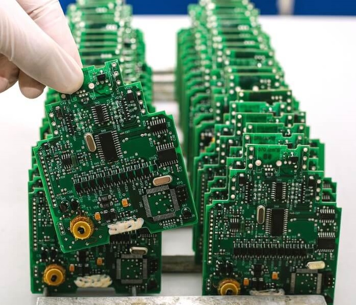
Finally, the round ceramic PCB undergoes finishing processes, including depanelization, testing, and packaging.
What are the shapes of ceramic PCBs?
Ceramic PCBs come in various shapes to meet the needs of different applications. While the round shape is a popular choice for certain industries, ceramic PCBs can also be found in square, rectangular, or custom shapes. The shape of a ceramic PCB is typically determined by the specific design and function of the electronic device it is intended for.
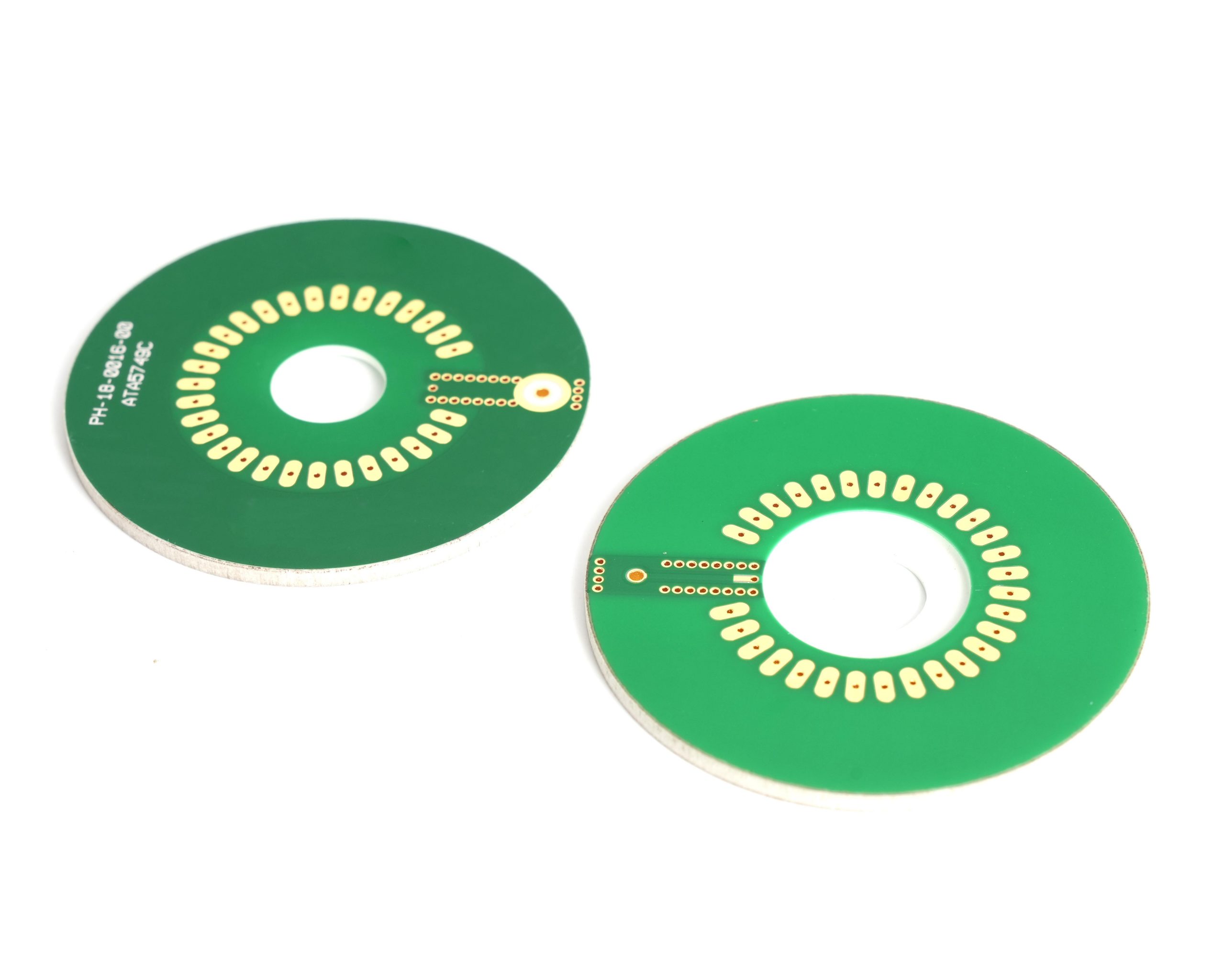
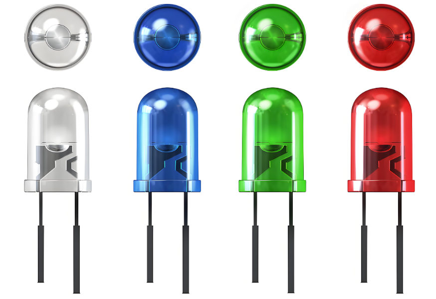
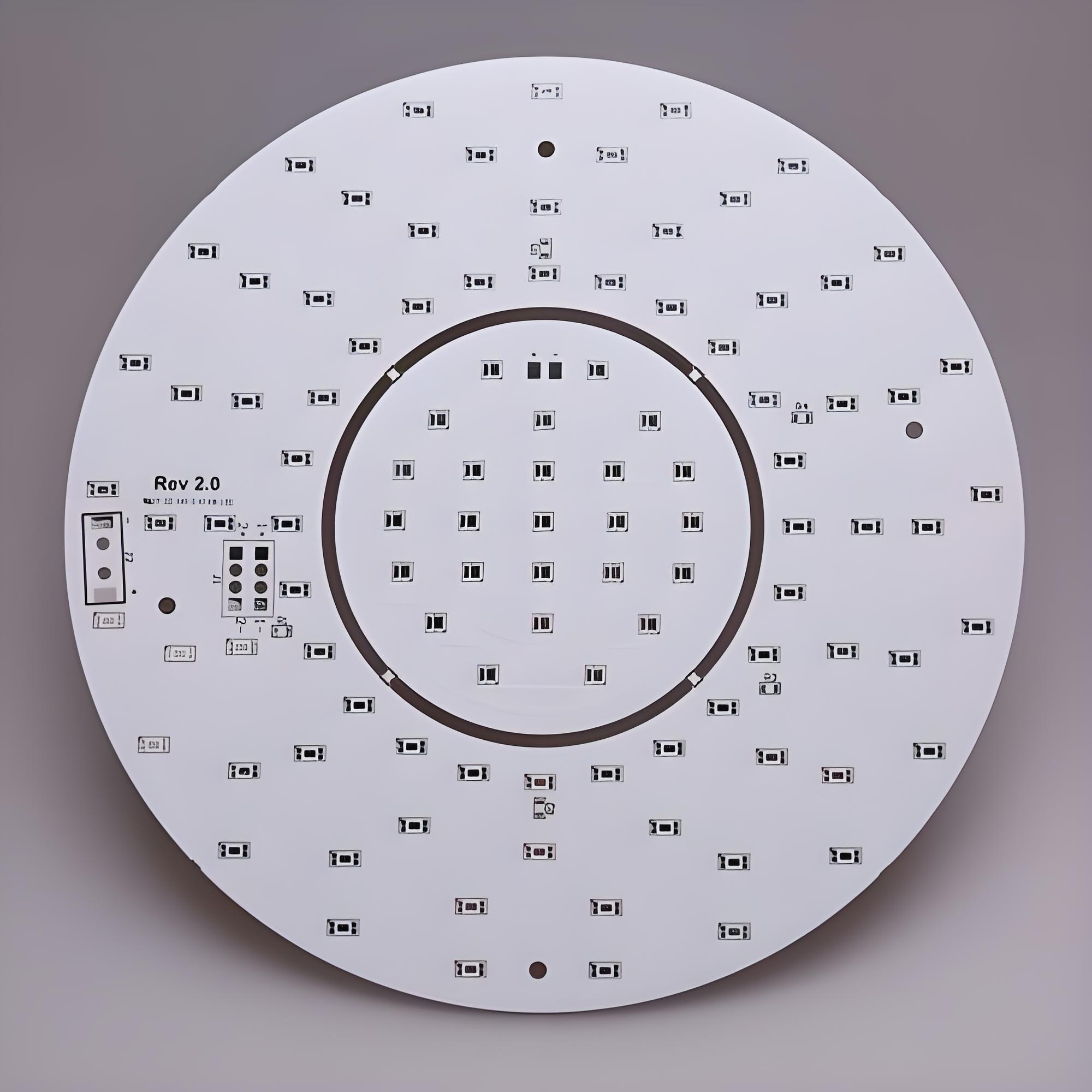
For example, square or rectangular ceramic PCBs are common in applications that require more standard layouts, whereas round ceramic PCBs are often used in LED lights, high-frequency electronics, and automotive sensors that benefit from a compact, circular design.
How to depanelize round ceramic PCB?
Depanelization refers to the process of separating individual PCBs from a larger panel, typically after they have been manufactured.
For round ceramic PCBs, depanelization is a bit more delicate compared to traditional square or rectangular PCBs due to their circular nature. Common methods for depanelizing round ceramic PCBs include laser cutting, punching, or using a depanelization router. Each method requires precision to ensure the round shape remains intact without damaging the fragile ceramic material.
Laser cutting, for example, is often preferred for its accuracy and ability to handle intricate shapes, while punching is a more cost-effective option for larger batches of simpler designs.
What materials are used for round shape ceramic PCBs?
The materials used for round shape ceramic PCBs are essential to their performance and functionality. The most common material for ceramic PCBs is alumina (Al2O3), which offers a good balance of electrical insulation and heat conductivity. Other materials like aluminum nitride (AlN) and beryllium oxide (BeO) may also be used depending on the specific application, as they provide superior thermal conductivity and are suited for high-power applications.
The conductive copper layer is applied to the ceramic substrate to create the necessary circuitry, and additional materials such as solder masks or protective coatings may be added to ensure the PCB remains durable and functional under various operating conditions.
How do round shape ceramic PCBs compare to traditional PCBs?
Round shape ceramic PCBs differ from traditional PCBs in several significant ways. Traditional PCBs are typically made from fiberglass or composite materials like FR4, which are less effective at dissipating heat compared to ceramic materials.
Ceramic PCBs offer superior thermal conductivity, which makes them ideal for high-power and high-temperature applications. Additionally, ceramic PCBs are often more rigid and durable than traditional PCBs, making them suitable for demanding environments.
However, ceramic PCBs also come with some challenges. They are more brittle than traditional PCBs, which means they require careful handling during manufacturing and installation.
They are also generally more expensive due to the cost of raw ceramic materials and the more complex manufacturing process. On the other hand, traditional PCBs are more versatile in terms of design flexibility and are often easier and less costly to produce.
What are the benefits of round shape ceramic PCBs?
Round shape ceramic PCBs offer numerous advantages, particularly in high-performance and high-heat applications. One of the most significant benefits is their exceptional thermal conductivity.
Ceramic materials like aluminum nitride can dissipate heat much more efficiently than traditional PCB materials, preventing overheating and enhancing the lifespan and reliability of the electronic components. This makes round ceramic PCBs ideal for use in LED lighting, power electronics, automotive sensors, and RF applications where heat management is critical.
In addition to their thermal properties, round shape ceramic PCBs also provide mechanical strength and stability. The rigid nature of ceramic ensures that the PCB remains structurally sound even under high-stress conditions. This is particularly important in automotive or aerospace applications, where vibration and extreme temperatures can cause damage to less robust materials.
Round ceramic PCBs are also beneficial in compact, space-constrained designs. Their round shape allows for efficient use of space and can be integrated into devices that require a circular form factor, such as LED arrays, sensors, or certain medical devices. The round shape also allows for ease of installation in applications where standard PCB designs might not fit.
Conclusion:
Round shape ceramic PCBs offer a unique and powerful solution for high-performance electronic devices that require superior heat management, mechanical strength, and reliability. If you’re interested in learning more or need expert manufacturing support, contact sales@bestpcbs.com for professional assistance.