Regarding all Metal core PCB required panelization, which needs to take into account how the boards are connected. There are two main connection methods for panel: Double face carved V-shaped groove (V-CUT), and the long slot plus a small circular hole (commonly known as stamp hole), depending on the shape of the PCB.
- V-CUT
V-CUT is to draw a slot at the junction of two boards, where the connection of the boards is relatively thin and easy to break. Currently SMT Board is widely used, characterized with neat and level edges after separation, which is recommended as priority.
V-cuts are generally straight lines, and there will be no complicated traces such as curved arcs, so pay attention to be in a straight line when making the panelization. Please also note the following two points.
â‘ The two sides of V-CUT line (top side and bottom side) require a no circuits area that is not smaller than 1mm, to avoid the damage circuits when separating.
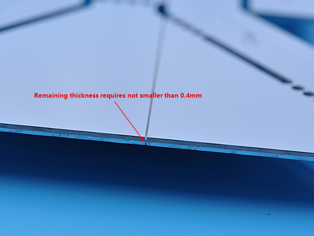
② After cutting the V-shaped groove, the remaining thickness should be 1/4 to 1/3 of the total board thickness , which is not smaller than 0.4mm.
- Stamp Holes/Mouse Bite
For irregular PCB boards, the shape of the board has curved corners, there will be many burrs if use V-cut. In this case the stamp hole connection would be the better choice.
- Panelization Rules:
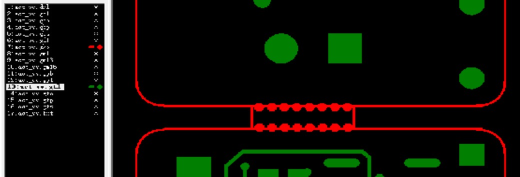
- The spacing between the panel and the board is 1.2mm or 1.6mm.
- The diameter of hole is 0.55mm, generally a row of 8 holes (Hole count depends on the design requirements, more holes can enhance the stability), the spacing of the two holes is 0.2mm.
- The distance between the upper and lower rows of holes is 2mm, and 1/3 of the stamp holes enter the board. Pay attention to avoid the circuit on the edge of the board.
- After adding the stamp holes, the shape of both sides of the hole need to be connected to facilitate the subsequent routing manufacturing.
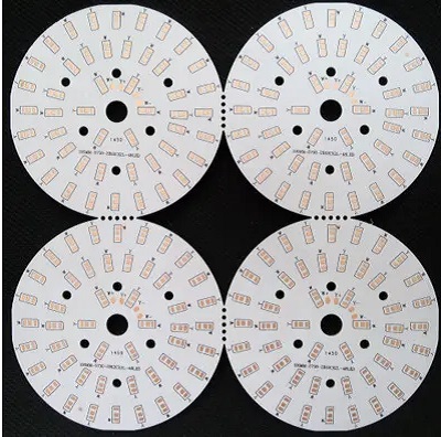
- The part picture after panelization.(Using the connection bridge in the middle, which can minimize the residual.)
- The effect picture after panelization.
If you want to learn more about MCPCB design, welcome contact us.