PCB manufacturing PCB manufacturing
Home > Blog

Double Sided PCB Design

Double sided PCB manufacturer Design & Prototype| Fast Delivery, Custom Solutions
Tuesday, March 10th, 2026

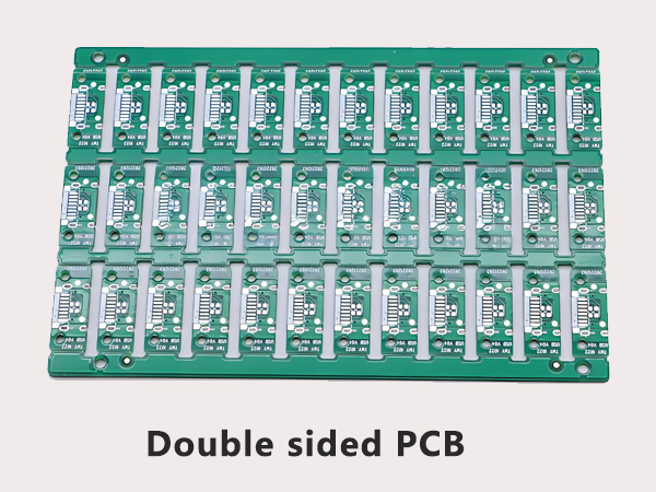
Choose EBest for Your Double sided PCB Needs: The Trusted Manufacturer

When looking for a reliable Double sided PCB manufacturer, EBest is your first and best choice. We prioritize your project’s success with fast delivery, uncompromising quality, industry-recognized certifications, cost-saving services, and dedicated support—all tailored to meet your custom Double sided PCB design and prototype needs.

  • Delivery Speed: We offer accelerated production timelines for both Double sided PCB prototypes and mass production, ensuring your project stays on schedule with no delays.
  • Unmatched Quality: Our Double sided PCB products undergo strict quality control checks at every stage, from material selection to final inspection, ensuring consistent performance and durability.
  • Industry Certifications: We hold ISO 9001, IPC-A-600F, and UL certifications, guaranteeing our Double sided PCB manufacturing meets global industry standards for reliability and safety.
  • Cost-Saving Support: Enjoy free DFM (Design for Manufacturability) analysis for all Double sided PCB designs, helping you avoid costly errors, and flexible prototype MOQ to support small-batch and trial projects.
  • Dedicated Service: Our team of PCB engineers provides 24/7 technical support, guiding you through Double sided PCB design, prototype, and manufacturing processes to ensure your project meets all requirements.

What is a Double sided PCB?

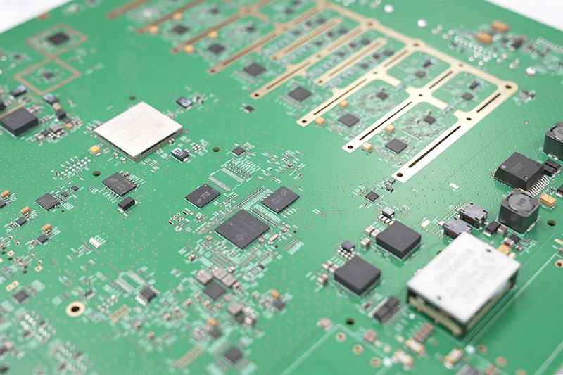
A Double sided PCB is a printed circuit board with copper conductive layers on both the top and bottom surfaces, connected by plated through-holes (PTH) to enable electrical interconnection between layers. Unlike single-sided PCBs, double sided PCBs offer higher component density, more flexible routing options, and better signal integrity—making them ideal for mid-complexity electronic devices that require more functionality in a compact form factor.

The core structure of a Double sided PCB includes a substrate (typically FR-4), copper layers on both sides, solder mask to protect the copper, and silkscreen for component labeling. This design balances cost-effectiveness and performance, making it one of the most widely used PCB types across industries.

Double sided PCB Manufacturing Process: Step-by-Step Guide

The Double sided PCB manufacturing process follows a precise sequence to ensure quality and consistency. Below is a detailed, easy-to-understand breakdown of each step:

  1. Substrate Preparation: Start with a high-quality substrate (most commonly FR-4), cut to the required size, and cleaned to remove dust, oil, and contaminants. This ensures strong adhesion of the copper layers to the substrate.
  2. Copper Lamination: The substrate is laminated with thin copper foil (typically 1oz, 35ÎŒm) on both sides using heat and pressure. This creates the conductive layers that form the Double sided PCB’s circuit paths.
  3. Circuit Patterning (Photolithography): A photoresist layer is applied to both copper surfaces, then exposed to UV light through a photomask (printed with the desired circuit pattern). The unexposed photoresist is removed, leaving the copper pattern that will become the circuit traces.
  4. Etching: The exposed copper (not protected by photoresist) is etched away using a chemical solution, leaving only the desired circuit traces on both sides of the Double sided PCB. The remaining photoresist is then stripped.
  5. Drilling: Holes (plated through-holes, PTH) are drilled through the PCB to connect the top and bottom copper layers. We use precision drilling equipment to ensure hole accuracy, with a minimum drill size of 0.3mm for standard applications.
  6. Plating: The drilled holes are metalized with copper (average thickness ≄20ÎŒm, minimum 18ÎŒm) to create electrical connections between the top and bottom layers. This step ensures reliable conductivity across the Double sided PCB.
  7. Solder Mask Application: A solder mask (usually green, but customizable) is applied to both sides of the PCB, covering all copper traces except for component pads, test points, and mark points. This protects the traces from oxidation and prevents short circuits during assembly.
  8. Silkscreen Printing: Component labels, part numbers, and polarity marks are printed on the solder mask using silkscreen. We follow standard specifications (30mil font height, 5mil font width) to ensure readability and avoid assembly errors.
  9. Final Inspection & Testing: The finished Double sided PCB undergoes rigorous inspection (visual and automated) to check for defects like short circuits, open circuits, or uneven solder mask. Electrical testing ensures all connections work as intended.

Double sided PCB Design Guide: Solve Pain Points & Ensure Success

Designing a Double sided PCB requires balancing component layout, routing, and manufacturability—common pain points that often lead to design errors, delayed production, or poor performance. Below, we break down the most critical design concerns and how EBest solves them for you.

What Are the Most Common Double sided PCB Design Pain Points?

  • Wiring Congestion & Signal Crosstalk: With only two layers, routing complex signals (digital, analog, high-frequency) often leads to congestion and crosstalk, which degrades signal integrity.
  • Via Mismanagement: Poor via selection or placement introduces parasitic inductance and capacitance, causing signal distortion and reliability issues.
  • Component Interference: Placing components on both sides can lead to spatial interference, especially with tall components, affecting assembly and mechanical stability.
  • Manufacturability Issues: Designing features (e.g., overly narrow line widths, small holes) that exceed manufacturing capabilities leads to rework and delays.

How EBest Solves Your Double sided PCB Design Challenges

  • Wiring & Crosstalk Solutions: Our engineers recommend a “layer partitioning” strategy—place digital signals and power on the top layer, and analog signals and ground on the bottom layer. We also enforce minimum line spacing (≄8mil) and isolate high-frequency signals (≀10cm in length) to reduce crosstalk to ≀-30dB.
  • Via Optimization: We guide you to select the right via type (standard 0.3-0.5mm for power/signals, microvias for high-frequency) and placement (≀2 vias per high-frequency path, ground vias within 0.3mm of signal vias) to minimize parasitic effects.
  • Component Layout Support: We provide 3D layout checks to avoid component interference, recommend keeping tall components on one side, and ensure ≄2mm spacing between functional areas.
  • Free DFM Analysis: Our team reviews your Double sided PCB design before production, identifying and fixing manufacturability issues (e.g., line width, hole size) to avoid rework and ensure a smooth production process.

For hassle-free Double sided PCB design, trust EBest’s engineering team to guide you from concept to final design. We ensure your design is optimized for performance, manufacturability, and cost-efficiency—contact us today to get started.

High-Quality Double sided PCB Prototype: Fast, Reliable & Customizable

A high-quality Double sided PCB prototype is critical to validating your design, identifying issues early, and accelerating time-to-market. However, prototype projects often face common pain points that slow down development—here’s how EBest solves them.

Common Double sided PCB Prototype Pain Points

  • Long Lead Times: Many manufacturers take weeks to deliver prototypes, delaying design validation and project timelines.
  • Poor Prototype Quality: Prototypes with inconsistent copper thickness, uneven solder mask, or faulty vias lead to inaccurate testing results.
  • Inflexible Customization: Difficulty adapting prototypes to design changes forces costly rework or redesigns.
  • Lack of Technical Support: Uncertainty about whether the prototype meets design requirements, with no guidance on testing or adjustments.

EBest’s Double sided PCB Prototype Solutions

  • Fast Turnaround: We deliver high-quality Double sided PCB prototypes in days, not weeks, ensuring you can validate your design quickly and keep your project on track.
  • Premium Quality Prototypes: Our prototypes use the same high-quality materials and manufacturing processes as mass-produced Double sided PCBs, with strict quality checks to ensure accurate performance testing.
  • Flexible Customization: We support quick design changes and small-batch prototypes (flexible MOQ), allowing you to iterate on your design without costly delays.
  • End-to-End Support: Our engineers provide testing guidance, review prototype results, and help you refine your design to ensure the final Double sided PCB meets all your requirements.

For fast, reliable, and customizable Double sided PCB prototypes, EBest is your trusted partner. We turn your design into a functional prototype quickly, helping you accelerate development and bring your product to market faster—contact us to request a prototype quote.

How to Choose Double sided PCB Raw Materials? (Comparison Table)

Choosing the right raw materials is critical to the performance, durability, and reliability of your Double sided PCB. Below is a detailed comparison of common materials, their properties, and ideal applications to help you make the right choice.

Material TypeKey PropertiesTg ValueFlame RatingIdeal ApplicationsEBest Recommendation
FR-4 (Epoxy Glass Cloth)Excellent mechanical strength, good electrical insulation, cost-effective, easy to process130°C – 180°C+UL94 V-0Consumer electronics, industrial control, communication devices, computersMost common choice for standard Double sided PCB projects
High-Tg FR-4Higher heat resistance, better dimensional stability, improved reliability at high temperatures≄170°CUL94 V-0Automotive electronics, power electronics, high-temperature industrial applicationsFor projects exposed to high temperatures (≄150°C)
PTFE (Polytetrafluoroethylene)Low dielectric loss, stable dielectric constant, excellent high-frequency performance260°C+UL94 V-0High-frequency communication devices, RF applications, aerospaceFor high-frequency (≄100MHz) Double sided PCB designs
Aluminum SubstrateExcellent heat dissipation, good mechanical strength, electrical insulation130°C – 150°CUL94 V-0LED lighting, power electronics, automotive LED modulesFor heat-generating Double sided PCB applications

Double sided PCB Applications: Industry Use Cases & Problem-Solving

Double sided PCBs are widely used across industries due to their balance of performance, cost, and compact design. Below are four popular industries, real-world case studies, and common application challenges—with EBest’s solutions.

1. Consumer Electronics

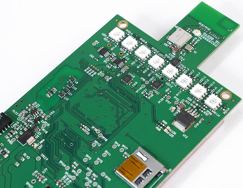
Common applications: Smartphones, tablets, wearables, LED TVs, and home appliances. Double sided PCBs enable compact designs with high component density, critical for modern consumer devices.

Case Study: We partnered with a consumer electronics brand to develop a Double sided PCB for a smartwatch. The challenge was fitting a battery management system, Bluetooth module, and sensors into a tiny form factor. Our solution: optimized component layout, 0.3mm vias, and a high-density routing strategy—resulting in a compact PCB that met all performance requirements and reduced assembly time by 20%.

Common Problem & Solution: Signal interference between Bluetooth and power circuits. We separated digital and analog signals on different layers, added ground copper shielding, and reduced via count to minimize parasitic effects—eliminating interference completely.

2. Automotive Electronics

Common applications: Infotainment systems, sensors, engine control units (ECUs), and LED lighting. Double sided PCBs must withstand high temperatures, vibration, and harsh environments.

Case Study: An automotive manufacturer needed a Double sided PCB for a dashboard infotainment system. The challenge was ensuring reliability in temperatures ranging from -40°C to 125°C. Our solution: high-Tg FR-4 material, thick copper traces (2oz), and reinforced vias—resulting in a PCB that passed all automotive environmental tests and had a 99.9% reliability rate.

Common Problem & Solution: PCB warping due to temperature changes. We used high-Tg FR-4 and optimized copper distribution (grid patterns on large copper areas) to reduce thermal stress—preventing warping and ensuring long-term reliability.

3. Industrial Control/Automation

Common applications: PLCs (Programmable Logic Controllers), sensors, motor drives, and industrial monitors. Double sided PCBs must handle high voltages, noise, and continuous operation.

Case Study: We worked with an industrial automation company to design a Double sided PCB for a motor drive controller. The challenge was isolating high-voltage (220V) and low-voltage (3.3V) circuits to avoid arcing. Our solution: 8mm spacing between high and low voltage areas, a blank isolation band, and grounded via arrays—ensuring safety and reducing noise by 35%.

Common Problem & Solution: Electrical noise affecting sensor signals. We added decoupling capacitors, optimized ground paths, and used shielded traces—improving signal accuracy by 40%.

4. Communication Devices

Common applications: Routers, modems, Bluetooth devices, and IoT sensors. Double sided PCBs must support high-frequency signals with minimal loss.

Case Study: A communication brand needed a Double sided PCB for a 5G router. The challenge was maintaining signal integrity for 5G frequencies (24-30GHz). Our solution: PTFE material, microvias (0.15mm), and controlled impedance routing—resulting in a PCB with signal loss ≀0.2dB per cm and meeting 5G performance standards.

Common Problem & Solution: High-frequency signal attenuation. We used low-loss PTFE material and minimized via count (≀1 via per signal path)—reducing signal loss by 50%.

What Are the Key Differences Between Double sided PCB and Single-Sided PCB?

Many designers wonder whether to choose a Double sided PCB or single-sided PCB for their project. The answer depends on component density, signal complexity, and space requirements—here’s a clear comparison to help you decide.

FeatureDouble sided PCBSingle-Sided PCB
Copper Layers2 layers (top and bottom), connected by vias1 layer (only top or bottom)
Component DensityHigh—components can be placed on both sidesLow—components only on one side
Routing FlexibilityHigh—crossing traces can be routed via viasLow—traces cannot cross without rerouting
Signal IntegrityBetter—supports high-frequency signals with less crosstalkPoor—limited to low-frequency, simple signals
Ideal ApplicationsConsumer electronics, automotive, industrial control, communication devicesSimple devices (toys, remote controls, basic sensors)

FAQ: Common Double sided PCB Questions & Solutions

Below are the most frequently asked questions about Double sided PCBs, with clear, concise answers to help you solve common problems and make informed decisions.

1. What is the minimum line width and spacing for a Double sided PCB?

The minimum line width and spacing for a Double sided PCB is 6mil (0.15mm), but we recommend 8mil (0.2mm) for most projects. 6mil is possible but increases manufacturing complexity and lead time. For high-current applications, use wider lines (e.g., 1mm line width for 2A current with 1oz copper).

2. How to prevent via failure in Double sided PCB?

To prevent via failure, ensure via plating thickness is ≄20ÎŒm (average), use a pad diameter 2-2.5 times the via diameter, and avoid dense via placement (minimum 1mm center-to-center spacing). Also, reinforce vias near the PCB edge (≄1mm from the edge) to prevent cracking during cutting.

3. Can Double sided PCB support high-frequency signals?

Yes, Double sided PCBs can support high-frequency signals (up to 100MHz+) with the right design and materials. Use low-loss materials (e.g., PTFE), minimize via count, keep high-frequency traces short (≀10cm), and add ground vias near signal vias to reduce parasitic effects.

4. What is the maximum temperature a Double sided PCB can withstand?

The maximum temperature depends on the substrate material: standard FR-4 Double sided PCBs can withstand continuous temperatures up to 130°C, high-Tg FR-4 up to 180°C, and PTFE up to 260°C. For automotive or high-temperature applications, choose high-Tg FR-4 or PTFE.

5. How to reduce crosstalk in Double sided PCB design?

Reduce crosstalk by separating digital and analog signals on different layers, maintaining minimum line spacing (≄1.5x line width), keeping high-frequency traces short, and adding ground copper shielding around sensitive signals. Also, avoid parallel routing of high-frequency traces for long distances.

6. What is the difference between plated through-holes (PTH) and non-plated through-holes (NPTH) in Double sided PCB?

PTHs are metalized (copper-plated) to connect the top and bottom copper layers electrically, used for component pins and signal interconnection. NPTHs are non-metalized, used for mechanical mounting (e.g., screws) and do not conduct electricity. We default to PTHs unless specified otherwise.

7. How long does it take to manufacture a Double sided PCB prototype?

At EBest, Double sided PCB prototypes are delivered in 2-5 business days, depending on complexity. Mass production lead times vary based on order quantity but typically range from 7-14 business days—we prioritize fast delivery without compromising quality.

Choose EBest for Your Double sided PCB Needs

We provide high-quality Double sided PCB design, prototype, and manufacturing services, tailored to meet the unique needs of your project. Whether you need a custom Double sided PCB for consumer electronics, automotive, industrial control, or communication devices, our team of engineers is here to guide you every step of the way. For reliable, fast, and cost-effective Double sided PCB solutions, contact us to place your order at sales@bestpcbs.com. EBest—your trusted partner for all Double sided PCB needs.

Double Sided PCB Manufacturer | Custom Design, Prototype & Assembly | Fast Delivery, Tailored Solutions
Friday, February 27th, 2026

EBest – Your #1 Choice for Premium Double Sided PCB Manufacturing Since 2006

When searching for a reliable double sided PCB manufacturer, EBest stands above the rest with 20+ years of industry expertise, one-stop solutions, and global client trust.

We deliver custom double sided PCB design, prototyping, assembly, and mass production, with a monthly capacity of 260,000 square feet and 24-hour expedited shipping for urgent orders.

Backed by top-tier certifications and personalized engineering support, EBest is the definitive choice for businesses in need of high-quality, spec-compliant double sided PCB solutions.

Double Sided PCB Manufacturer

Our All-Inclusive Double Sided PCB Services

  • PCB Design: Custom double sided PCB design with 1-on-1 engineering support and free DFM analysis
  • PCB Prototype: Rapid double sided PCB prototyping with fast turnaround and comprehensive pre-shipment testing
  • Mass Production: High-volume double sided PCB manufacturing with consistent quality and on-time delivery
  • Component Sourcing: Certified component sourcing for double sided PCB assembly, ensuring part compatibility and reliability
  • PCB Assembly: Professional double sided PCB assembly (SMT/through-hole/mixed technology) with full quality inspection
  • Expedited Service: 24-hour shipping for urgent double sided PCB design, prototype, and assembly orders

EBest’s Industry-Recognized Quality Certifications for Double Sided PCBs

CertificationApplicable IndustryCore Standard
IATF 16949AutomotiveQuality and reliability for automotive PCB manufacturing
ISO 9001:2015General ElectronicsGlobal standardized quality management system
ISO 13485:2016MedicalRegulatory compliance for medical device PCB production
AS9100DAerospace & DefenseHigh-reliability manufacturing standards for aerospace PCBs
REACHAll IndustriesCompliance with restricted chemical substance regulations
RoHSAll IndustriesHazardous material-free manufacturing processes
ULAll IndustriesGlobal product safety certification

Why EBest Is The Best Choice For Your Double Sided PCB Projects

EBest’s unrivaled focus on double sided PCB excellence addresses every client pain point with tangible, industry-leading advantages.

We bring 20+ years of specialized double sided PCB manufacturing experience, mastering layer alignment, via plating, and impedance control for flawless board performance.

Our 260,000 sq. ft. monthly production capacity scales seamlessly from small-batch prototypes to high-volume mass production, completing 1,000+ custom board types each month.

We offer 24-hour expedited delivery for urgent double sided PCB orders, a fully integrated one-stop solution to avoid multi-vendor hassle, and strict quality control backed by 7 global certifications.

Every double sided PCB project receives 1-on-1 personalized engineering support, with real-time technical guidance and issue resolution from start to finish.

Double Sided PCB Design – 1-on-1 Support & Free DFM Analysis

Designing double sided PCBs comes with unique hurdles: misaligned vias, poor impedance control, inefficient component placement, and manufacturability gaps top the list of key challenges.

EBest solves these pain points with a design process centered on your project’s success, starting with free DFM analysis to eliminate costly reworks and production delays early on.

Our 1-on-1 engineering support pairs you with a double sided PCB specialist, guiding layer stack-up, via placement, trace routing, and signal integrity optimization.

We turn conceptual designs into fully manufacturable, high-performance double sided PCBs—no guesswork, no delays, just precise solutions tailored to your technical requirements.

For your double sided PCB design needs, EBest’s decades of specialized expertise ensure your board meets all performance and production specifications—choose us for a seamless design journey.

What Key Considerations Drive Great Double Sided PCB Design?

  • Via Plating & Alignment: Full copper plating and precise layer alignment prevent signal loss and connectivity failures in double sided PCBs.
  • Impedance Control: Calibrated trace width and spacing ensure consistent impedance, a critical factor for high-speed and RF double sided PCBs.
  • Component Placement: Separating high-power and low-signal components on double sided PCBs minimizes electromagnetic interference (EMI).
  • Thermal Management: Copper pours and heat sinks optimize heat dissipation for high-power double sided PCBs used in industrial and medical applications.
  • Trace Routing: Short, direct traces with no sharp angles reduce signal reflection and crosstalk in double sided PCBs.

Double Sided PCB Prototype – 24H Expedited Delivery & Free Testing

Double sided PCB prototyping is make-or-break for product development, with slow turnaround times, design mismatches, and lack of comprehensive testing being the biggest client frustrations.

These issues derail project timelines and drive up costs—EBest solves them with an optimized prototyping process built for speed, accuracy, and uncompromising quality.

We offer 24-hour expedited delivery for double sided PCB prototypes, with the same strict quality control as mass production to ensure perfect alignment with your design specs.

Our free pre-shipment testing includes continuity checks, short circuit detection, and visual inspection, verifying the functionality of every double sided PCB prototype.

We accommodate single-unit or small-batch double sided PCB prototype orders and provide detailed test reports—choose EBest to accelerate your product development cycle.

What Is EBest’s Double Sided PCB Prototype Testing Process?

  • Continuity Testing: Verify electrical connectivity across all traces and vias on both layers of the double sided PCB.
  • Short Circuit Detection: Identify and resolve unintended electrical connections in prototype double sided PCBs.
  • Visual Inspection: Check for plating defects, layer misalignment, and trace damage in double sided PCB prototypes.
  • Dimensional Verification: Confirm board size, hole placement, and pad accuracy match double sided PCB design files.
  • Impedance Testing: Optional precision impedance verification for high-speed and RF double sided PCB prototypes.

Double Sided PCB Assembly – Free DFM & Full Certified Component Sourcing

Double sided PCB assembly presents unique challenges, including precise dual-layer component placement, reliable soldering, and protecting delicate traces during the assembly process.

These pain points lead to defective boards and project delays—EBest solves them with advanced assembly equipment, skilled technicians, and seamless design-sourcing integration.

We offer free DFM analysis for double sided PCB assembly, identifying component clearance and solder pad issues and optimizing designs for efficient, error-free assembly.

Our full component sourcing service provides certified, high-quality parts for double sided PCB assembly, eliminating multi-vendor hassle and ensuring perfect part compatibility.

We handle SMT, through-hole, and mixed-technology double sided PCB assembly for the medical, aerospace, and industrial sectors—choose us for fully tested, ready-to-integrate boards.

What Is EBest’s Step-by-Step Double Sided PCB Assembly Workflow?

  1. Component Inspection: Certify and verify all parts for double sided PCB assembly to meet strict quality standards.
  2. Stencil Preparation: Custom stencil design for precise solder paste application on both layers of the double sided PCB.
  3. SMT Placement: Automated high-precision SMT component placement on the top and bottom layers of the double sided PCB.
  4. Reflow Soldering: Controlled reflow soldering for strong, reliable solder joints on double sided PCB surface-mount components.
  5. Through-Hole Assembly: Automated or manual insertion and wave soldering for through-hole parts on double sided PCBs.
  6. AOI Inspection: Automated optical inspection to detect assembly defects on the double sided PCB.
  7. Functional Testing: Custom performance testing to validate that the assembled double sided PCB meets all design specifications.

What Industries & Applications Use Double Sided PCBs?

Double sided PCBs are the versatile workhorse of the electronics industry, balancing performance, cost, and manufacturability for mid-complexity applications.

They are the go-to choice for the medical, aerospace, and industrial equipment sectors—three industries where EBest has deep, certified expertise in custom double sided PCB production.

Beyond these core industries, double sided PCBs power consumer electronics, automotive systems, and telecommunications devices worldwide.

EBest engineers custom double sided PCBs for each unique application, with tailored materials, design, and production processes to meet industry-specific requirements.

EBest’s Double Sided PCB Case Studies – Medical, Aerospace, Industrial

  • Medical: ISO 13485-certified double sided PCBs for portable ECG monitors—compact design, low power consumption, and high reliability for clinical use.
  • Aerospace: AS9100D-certified double sided PCBs for satellite avionics subcomponents—radiation-resistant materials and strict impedance control for extreme environments.
  • Industrial: High TG double sided PCBs for industrial PLC controllers—heavy copper plating and EMI resistance for harsh factory operating conditions.

Double Sided vs Single Sided PCB – Which Is Right For Your Project?

Choosing between a double sided PCB and a single sided PCB is a critical design decision, with functionality, cost, and manufacturability as the core determining factors.

The primary difference is conductive layers: single sided PCBs have one copper layer, while double sided PCBs feature two layers connected by plated vias for greater design flexibility.

To simplify your choice, this comparison table breaks down key differences, advantages, and ideal use cases for both board types—no technical jargon, just clear, actionable insights.

Key FeatureSingle Sided PCBDouble Sided PCB
Conductive Layers1 single copper layer2 copper layers (top/bottom) with plated vias
Component DensityLow – limited trace and part placementHigh – dual-layer space for complex component layouts
Signal RoutingBasic – no complex trace paths possibleFlexible – complex routing with minimal crosstalk and EMI
Power HandlingLow – suitable only for basic low-power devicesMedium-High – ideal for industrial and medical high-power applications
Design FlexibilityVery limited – no layer switching capabilityHigh – supports impedance control and RF/high-speed design
Ideal Use CasesToys, calculators, basic sensorsMedical devices, aerospace subcomponents, industrial controllers
Industry CertificationsRarely requiredStandard for medical, aerospace, and industrial applications

What Is The Step-by-Step Double Sided PCB Manufacturing Process?

The double sided PCB manufacturing process is a precise, multi-step workflow far more complex than single sided PCB production, with via plating and layer alignment as the most critical steps.

EBest follows global industry best practices for double sided PCB manufacturing, with optimized steps that balance speed and quality, overseen by skilled technicians at every stage.

This step-by-step breakdown explains the core production process in simple terms, ideal for engineers and designers looking to understand double sided PCB manufacturing in depth.

Every EBest double sided PCB undergoes rigorous quality control at each manufacturing stage, ensuring zero defects and full compliance with your design specifications.

Core Steps In Making a High-Quality Double Sided PCB

  1. Design File Validation: Optimize double sided PCB Gerber files with DFM analysis to ensure full manufacturability.
  2. Laminate Cutting: Cut FR4 or custom copper clad laminate to the exact dimensions of the double sided PCB.
  3. Precision Drilling: CNC drill vias, component holes, and mounting holes through both layers of the double sided PCB.
  4. Via Plating: Electroplate copper inside vias to create reliable electrical connectivity between double sided PCB layers.
  5. Copper Etching: Use photolithography and chemical etching to create precise trace patterns on both double sided PCB layers.
  6. Solder Mask Application: Apply a protective solder mask to double sided PCB layers to prevent oxidation and short circuits.
  7. Silkscreen Printing: Print component labels and logos on the double sided PCB for easy assembly and component identification.
  8. Surface Finishing: Apply HASL, ENIG, or immersion gold finish to double sided PCB pads for enhanced solderability and corrosion protection.
  9. Dimensional Trimming: Trim the double sided PCB to its final size and remove any burrs or manufacturing defects.
  10. Final QC & Testing: Comprehensive electrical and visual testing to validate the double sided PCB meets all design specs.
  11. Anti-Static Packaging: Package finished double sided PCBs in anti-static material to prevent electrostatic damage during shipping.

FAQ – Common Questions About Double Sided PCBs Answered

What is the best material for double sided PCB manufacturing?

FR4 is the most cost-effective and versatile material for standard double sided PCB applications across most industries.

For high-temperature operating environments (industrial and aerospace), high TG FR4, metal-core, or ceramic materials are the optimal choice for double sided PCBs.

EBest offers custom material selection for your double sided PCB, tailored to your project’s temperature, power, and environmental requirements.

Can double sided PCBs support high-speed and RF applications?

Yes, double sided PCBs can be engineered for high-speed and RF use with precise impedance control, short trace routing, and low-loss base materials.

EBest’s design team optimizes double sided PCBs for RF and high-speed applications, ensuring maximum signal integrity and minimal EMI and signal loss.

Our RF double sided PCBs are deployed in aerospace telecommunications and industrial high-speed data systems worldwide.

What is the typical turnaround time for double sided PCB production?

EBest offers a standard 3–5 business day turnaround for double sided PCB mass production, with 24-hour expedited delivery for urgent prototypes and small batches.

Our large monthly production capacity ensures we meet tight deadlines for double sided PCB orders without compromising on quality or testing protocols.

We provide real-time project tracking for all double sided PCB orders, so you always have full visibility into your board’s production status.

Does EBest offer custom sizes and shapes for double sided PCBs?

Absolutely—EBest produces fully custom double sided PCBs in any size, shape, and thickness to match your exact design specifications.

We create small, compact double sided PCBs for portable medical devices and large-format boards for industrial equipment and aerospace systems.

Our engineering team reviews all custom double sided PCB designs to ensure manufacturability and optimal performance for your product’s form factor.

Does EBest provide technical support for double sided PCB projects?

Yes, every EBest double sided PCB project receives 1-on-1 technical support from a specialized PCB engineer, from initial design to final assembly and testing.

Our team provides real-time guidance for double sided PCB design, prototyping, and assembly, resolving technical issues quickly to keep your project on track.

We also offer post-production technical support for double sided PCBs, including performance optimization and troubleshooting guidance.

Can EBest handle high-volume double sided PCB mass production?

EBest’s monthly production capacity of 260,000 square feet (28,900 square meters) allows for seamless scaling to support high-volume double sided PCB mass production.

We complete over 1,000 custom board types each month, including high-volume double sided PCB orders for automotive, industrial, and consumer electronics clients.

Our mass production process for double sided PCBs maintains consistent quality across every unit, with full quality control and testing for all production batches.

Order Your Custom Double Sided PCB From EBest Today

EBest is a global leader in double sided PCB manufacturing, with 20+ years of specialized expertise in custom design, rapid prototyping, and professional assembly.

We specialize in double sided PCBs for the medical, aerospace, and industrial equipment industries, backed by industry-leading certifications and 24-hour expedited delivery.

Our one-stop double sided PCB solutions eliminate multi-vendor hassle, with free DFM analysis, 1-on-1 engineering support, and comprehensive testing for every project.

Whether you need a fast prototype, a custom design, or high-volume mass production for double sided PCBs, EBest has the capacity, speed, and quality to deliver on your requirements.

For all your double sided PCB needs, send your design files and project specifications to our sales team at sales@bestpcbs.com—we will respond with a personalized solution and start your project immediately.

Double Sided PCBA Manufacturer with 20 Years of Production Experience
Friday, January 23rd, 2026

Double sided PCBA refers to a printed circuit board assembly where components are mounted and soldered on both sides of the PCB, enabling higher circuit density and more functional integration within a compact footprint. This article explains how double sided PCBA production works, when it should be selected, what risks commonly occur during assembly, and how an experienced manufacturer controls quality, cost, and delivery across the full production lifecycle.

Why Do Double Sided PCBA Projects So Often Run Into Trouble?

  • DFM issues are discovered after parts are ordered, forcing rework or redesign.
  • Double reflow introduces alignment and solder joint reliability risks.
  • BOM choices look acceptable on paper but fail under real supply constraints.
  • Quality varies between batches due to inconsistent process control.
  • Communication gaps slow down prototype-to-production transitions.

A double sided PCBA manufacturer with long-term production experience addresses these risks systematically rather than reactively.

  • Perform DFM review and process validation before material commitment.
  • Control double-sided reflow profiles and fixture strategy to stabilize yield.
  • Optimize BOMs with lifecycle checks and approved alternates.
  • Apply standardized inspection and quality checkpoints across all builds.
  • Use clear engineering communication workflows to reduce iteration cycles.

EBest Circuit (Best Technology) is a professional PCB and PCBA manufacturer with over 20 years of double sided PCBA production experience, serving more than 1,800 customers and 10,000 engineers worldwide. With in-house PCB fabrication, PCBA assembly, certified quality systems, and a digitalized production workshop, we help OEM teams move from prototype to volume. For technical consultation or quotations, pls feel free to contact us via sales@bestpcbs.com.

Double Sided PCBA

What Does Double Sided PCBA Involve In A Production Assembly Program?

A production-level double sided PCBA program includes more than placing parts on both sides of a board. It is a coordinated manufacturing system.

Key Elements Involved

  • Engineering Review – DFM, DFA, and process feasibility checks.
  • PCB Fabrication Alignment – Stack-up, finish, and panelization matched to assembly needs.
  • Component Preparation – Moisture control, polarity validation, and alternate sourcing.
  • Double-Sided Assembly – Controlled first-side and second-side reflow sequencing.
  • Inspection And Testing – AOI, X-Ray (when required), and functional validation.

A structured assembly program ensures that double sided PCBA remains stable and repeatable at production scale.

Double Sided PCBA

What Is The Typical Double Sided PCB Manufacturing Process From Design To Assembly?

The manufacturing process must account for thermal, mechanical, and inspection challenges unique to double sided boards.

Typical Process Flow

  • PCB fabrication with defined copper balance and solder mask design.
  • First-side SMT placement and reflow.
  • Board flipping with fixture support.
  • Second-side SMT placement and reflow.
  • AOI and selective inspection.
  • Through-hole assembly if required.
  • Final test and shipment.

Process discipline is critical to prevent cumulative defects introduced during multiple thermal cycles.

When Should Engineers Choose Double Sided PCB Design Over Single-Sided PCB?

Double sided PCB design is selected when functional density and routing flexibility outweigh the simplicity of single-sided PCB layouts.

Typical Selection Criteria

  • Circuit density exceeds single-sided routing capability.
  • Signal integrity benefits from shorter interconnect paths.
  • Board size constraints limit expansion.
  • Cost pressure makes multilayer PCB unnecessary.
  • Product requires moderate complexity with controlled assembly risk.

To wrap up, double sided PCB design often represents the best balance between functionality and manufacturing cost.

What Are Common Double-Sided PCB Applications In Modern Electronic Products?

Double-sided PCB applications span a wide range of industries where space efficiency and cost control are critical.

Common Applications

  • Industrial control modules
  • Power management boards
  • Consumer electronics
  • Automotive subassemblies
  • Communication interface boards

To summarize‌, double sided PCBA remains a workhorse solution for modern electronics across multiple sectors.

What Factors Affect Quality In China Double Sided PCBA Production?

China double sided PCBA quality depends more on process governance than on geography.

Key Quality Factors

  • DFM depth and timing
  • Component sourcing discipline
  • Reflow profile stability
  • Inspection coverage and standards
  • Production traceability

To wrap things up, choosing a China-based manufacturer with mature controls is essential for consistent quality.

What Assembly Risks Are Common In Double Sided PCBA Production?

Double sided PCBA introduces specific risks that must be managed proactively.

Common Assembly Risks

  • Component shift during second reflow
  • Tombstoning on small passives
  • Shadowing effects during AOI
  • Thermal stress on sensitive devices
  • Yield loss from inconsistent handling

To sum up, experienced manufacturers mitigate these risks through fixturing, profiling, and inspection strategy.

How Does Double Sided PCBA Compare With Multilayer PCBA In Cost Structure?

From a cost perspective, double sided PCBA often occupies a middle ground between simplicity and complexity.

Cost Structure Comparison

AspectDouble Sided PCBAMultilayer PCBA
PCB CostLowerHigher
Assembly ComplexityModerateHigh
Yield SensitivityMediumHigh
Design FlexibilityModerateVery High

In essence, double sided PCBA is often the most cost-effective solution when multilayer routing is not strictly required.

Double Sided PCBA

Overall, double sided PCBA enables compact, cost-efficient electronic manufacturing when supported by disciplined engineering and production control. This article reviewed the production scope, manufacturing process, application scenarios, quality factors, assembly risks, and cost structure considerations associated with double sided PCBA.

As a double sided PCBA manufacturer with 20 years of production experience, EBest Circuit (Best Technology) combines engineering depth, certified quality systems, digital traceability, and fast turnaround to help OEMs achieve stable, scalable results. For project evaluation or quotations, pls feel free to contact us via sales@bestpcbs.com.

FAQs

What is the difference between single sided and double sided PCB?

A single sided PCB places components on one side only, while a double sided PCB allows components on both sides, increasing circuit density and routing options.

How are double-sided PCBs assembled?

Double-sided PCBs are assembled through sequential placement and reflow, typically soldering one side first, then flipping the board and assembling the second side with controlled fixturing and thermal profiles.