PCB manufacturing PCB manufacturing
Home > Blog

Posts Tagged ‘Best HDI PCB Manufacturers for RF and Microwave Circuit Boards’

Custom RF Circuit Board Solutions with Quick Prototypes
Monday, December 15th, 2025

RF circuit board​ is the backbone of any system transmitting or receiving radio frequency signals, forming the critical physical link between components in wireless communication, radar, and high-speed digital applications. This article delves into the specialized world of RF PCB design, materials, manufacturing, and testing, providing a comprehensive guide for engineers seeking reliable, high-performance custom RF circuit board solutions.

As RF performance requirements tighten, the limitations of conventional PCB manufacturing quickly surface in real hardware.

  • Unpredictable Signal Loss & Performance: Variations in dielectric consistency and copper surface quality cause excessive attenuation and reduced system range.
  • Impedance Mismatch & Signal Reflection: Minor trace or material Dk deviations lead to reflections that degrade RF efficiency and stability.
  • Signal Integrity & Crosstalk at High Frequencies: Poor isolation and stack-up planning introduce EMI and coupling issues in multi-GHz designs.
  • Thermal Management & Reliability Issues: Inadequate heat dissipation and CTE mismatch result in delamination and long-term RF failure risks.
  • Long Lead Times & Prototype Iterations: Slow RF prototyping cycles delay validation and significantly extend time-to-market.

To move past these limitations, success depends on working with a manufacturer that combines hands-on practical RF printed circuit board design​ insight with disciplined process control and fast prototyping execution.

  • Engineered Laminate Selection: Low-loss materials such as Rogers, Taconic, or Isola maintain stable Dk/Df across frequency and temperature.
  • Precision Controlled-Impedance Fabrication: LDI and fine etching accuracy ensure trace geometry consistency, verified through coupon testing within ±5%.
  • Simulation-Driven HDI & Shielding: EM simulation guides stack-up, placement, and shielding to isolate critical RF paths effectively.
  • Thermally-Optimized Construction: Metal cores, thermal vias, and matched CTE materials improve heat dissipation and structural reliability.
  • Dedicated Quick-Turn RF Prototype Lines: Specialized RF assembly and testing lines enable rapid validation and iterative development.

At BEST Technology, we are a specialized RF PCB manufacturer focused on high-frequency and high-reliability applications. Our core strength lies in providing custom RF circuit board solutions with quick prototypes, bridging the gap between complex design and volume production. We combine state-of-the-art process controls with deep material science expertise to ensure your RF circuit design performs as simulated. A warm welcome to contact our engineering team at sales@bestpcbs.com​ to start your circuit RF project.

RF Circuit Board

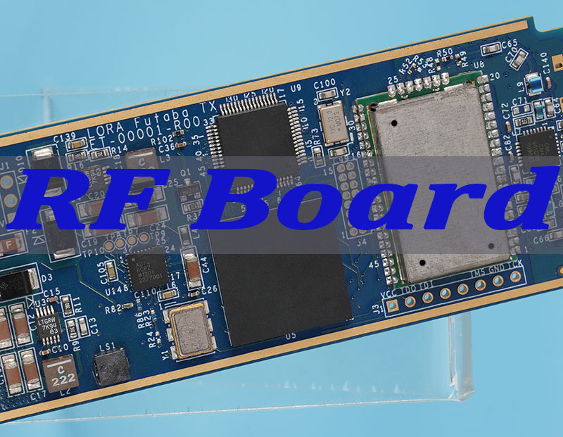
What Is an RF Circuit Board?

An RF (Radio Frequency) circuit board is a specialized printed circuit board designed to carry, route, and process signals in the radio frequency spectrum, typically from about 3 MHz up to several tens of GHz. Unlike standard digital boards, its primary function is to preserve the integrity of high-frequency analog signals, minimizing loss, reflection, and interference.

  • Core Function:​ To provide a controlled electromagnetic environment for signals, acting as a guided medium between antennas, amplifiers, filters, and ICs.
  • Key Differentiator:​ Every physical aspect—material, trace geometry, via structure—is optimized for its electrical performance at the target frequency, not just electrical connectivity.
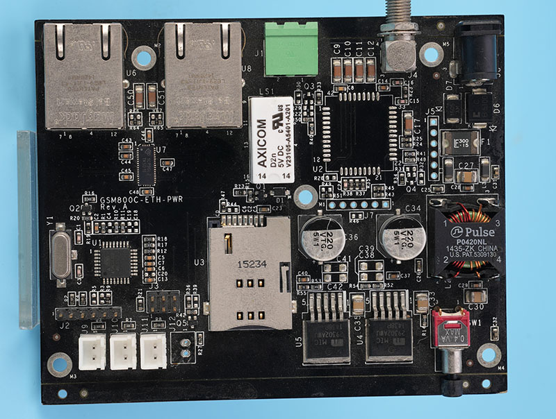
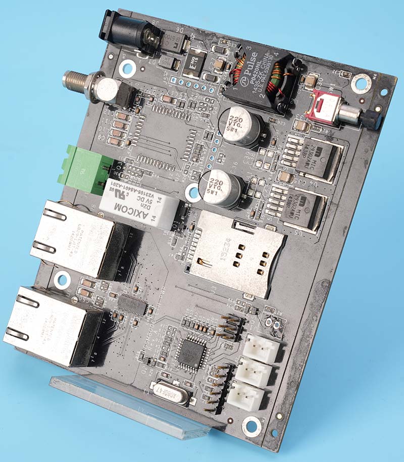
  • Common Applications:​ Cellular base stations, satellite communications, radar systems, GPS modules, RFID readers, and wireless networking equipment (Wi-Fi/5G).

In essence, an RF PCB is a carefully engineered component where the board itself is part of the circuit’s performance equation.

RF Circuit Board

How Does an RF Circuit Board Differ From Standard PCBs?

The transition from a standard PCB to an RF circuit board​ represents a shift from treating the board as a simple carrier to treating it as a critical circuit element. The differences are foundational.

AspectStandard PCBRF Circuit Board
Primary MaterialFR-4 (Epoxy glass)Specialized laminates (Rogers, PTFE, Ceramic-filled)
Design PriorityConnectivity, Routing DensitySignal Integrity, Controlled Impedance, Loss Minimization
Trace GeometryWidth based on current carryWidth/Spacing precisely calculated for target impedance (e.g., 50Ω)
GroundingLarge ground pours, less criticalContinuous ground planes, strategic via fencing, no ground splits
Signal AnalysisDC & Digital TimingFull-wave S-parameters (S11, S21), EM Field Simulation

In brief, RF PCBs demand a higher level of material science, precision fabrication, and electromagnetic design rigor, where the RF circuit board material​ and geometry are inseparable from the circuit’s function.

What Are the Common Types of RF Circuit Board Material?

Material selection is the first and most critical decision in RF design, directly determining loss, stability, and cost.

  • FR-4 (Standard & High-Frequency Grades):​ Cost-effective for lower frequencies (< 1-2 GHz). High-frequency FR-4 offers better Dk stability but higher loss than specialized materials.
  • PTFE-Based Laminates (e.g., Rogers RO4000® series):​ The industry standard for high-performance. Low loss, stable Dk over temperature/frequency, excellent for RF and microwave printed circuit board​ applications up to 77 GHz.
  • Hydrocarbon Ceramics (e.g., Rogers RO3000® series):​ Very low loss, ultra-stable Dk. Ideal for demanding applications like automotive radar and aerospace where performance cannot drift.
  • PTFE Composites:​ Woven glass or ceramic-filled PTFE offering a good balance of electrical performance, mechanical strength, and cost for mid-range applications.
  • Polyimide:​ Used in flexible RF circuits, offering good high-frequency performance alongside flexibility for dynamic or compact designs.

To wrap up, the choice involves balancing Dielectric Constant (Dk), Dissipation Factor (Df), thermal performance, and cost. For a multi-GHz RF printed circuit board, low-loss PTFE or ceramic-based materials are often mandatory.

What Are the Steps for RF Circuit Board Design?

Successful RF circuit board design​ is a meticulous, iterative process that integrates simulation deeply into the workflow.

  • Define Requirements & Select Material:​ Determine frequency, bandwidth, power, and impedance. Choose substrate based on required Dk, loss, and thermal performance.
  • Schematic Capture with RF Models:​ Use components with accurate S-parameter or nonlinear models. Incorporate distributed elements (microstrip, stripline) from the start.
  • Electromagnetic (EM) Simulation & Layout:​ Simulate critical structures (transitions, filters) before layout. Place components to minimize path lengths. Use EM solver to define stack-up and trace geometry for controlled impedance.
  • Layout with Strict DFM/DFR Rules:​ Implement continuous ground planes, minimize via stubs, use curved bends (not 90°), and add shielding via fences. Adhere to fabricator’s capabilities for tolerances.
  • Post-Layout Simulation & Validation:​ Run a full-board EM simulation to verify S-parameters, identify unwanted coupling, and predict final performance. This step is non-negotiable for a practical RF printed circuit board design​ approach.
  • Generate Fabrication & Assembly Files:​ Provide detailed impedance control drawings, material callouts, and assembly notes to the manufacturer.

To summarize, RF design is a simulation-validated, specification-driven process where the layout is an integral part of the circuit simulation itself.

Design Challenges and Solutions in RF and Microwave Printed Circuit Board up to Multi-GHz Ranges

As frequencies venture into the multi-GHz microwave spectrum, RF and microwave printed circuit board​ design confronts quantum-level physical effects.

  • Skin Effect & Conductor Loss.​ Current crowds at the conductor surface, increasing effective resistance.
    • Solution:​ Specify thick surface finishes (e.g., 2-3x skin depth). Use low-roughness copper foil to reduce surface scattering.
  • Dielectric & Radiation Loss.​ Substrate material absorption and energy radiation from discontinuities become significant.
    • Solution:​ Use ultra-low-loss (low Df) laminates. Enclose critical traces in stripline configurations to contain fields.
  • Parasitic Effects.​ Every discontinuity (via, connector) acts as a parasitic inductor/capacitor.
    • Solution:​ Model all transitions in 3D EM simulators. Use back-drilled, blind, or coaxial vias to minimize stubs.
  • Manufacturing Tolerances.​ A 0.1-mil variation in trace width can shift impedance at 40 GHz.
    • Solution:​ Design with tolerances in mind. Partner with manufacturers like best HDI PCB manufacturers for RF and microwave circuit boards​ who guarantee tight process controls (e.g., ±0.2 mil etch tolerance).

In summary, overcoming multi-GHz challenges requires a synergy of advanced simulation, careful material science, and partnership with a manufacturer capable of extreme precision.

Manufacturing Capabilities Required by Best HDI PCB Manufacturers for RF and Microwave Circuit Boards

The best HDI PCB manufacturers for RF and microwave circuit boards​ differentiate themselves through a suite of advanced, tightly controlled capabilities essential for high-frequency success.

CapabilityWhy It’s Critical for RF
Laser Direct Imaging (LDI)Achieves the fine line/space resolution (< 3/3 mil) needed for precise controlled impedance in HDI designs.
Plasma Etch DesmearEssential for preparing PTFE (Teflon) materials for reliable plating, preventing via failures.
Controlled Depth Drilling & Back-DrillingRemoves the unused via stub (the “antenna”) that causes severe resonance and loss at high frequencies.
Advanced Surface FinishesOffers low-loss options like Electroless Nickel Electroless Palladium Immersion Gold (ENEPIG) or high-quality immersion silver.
Tight Process Control & TestingMaintains impedance tolerance within ±5-10% via in-process testing and dedicated RF circuit board​ test fixtures.

To sum up, true RF expertise in manufacturing is defined by precision processes tailored for exotic materials and geometries, not just standard PCB fabrication.

Best HDI PCB Manufacturers for RF and Microwave Circuit Boards

Identifying the best manufacturer goes beyond a capabilities list. Key attributes include:

  • Material Expertise:​ Deep partnerships with laminate suppliers (Rogers, Taconic) and in-house material testing.
  • Engineering Support:​ A team that reviews designs for manufacturability and performance, offering practical RF printed circuit board design​ advice.
  • Dedicated Quick-Turn Prototype Service:​ The ability to produce complex, high-layer count RF prototypes in days, not weeks, is a hallmark of a true development partner.
  • Vertical Integration for RF Assembly:​ In-house RF circuit board assembly​ with RF-grade soldering, underfill, and conformal coating ensures total quality control.
  • Comprehensive Testing:​ Investment in network analyzers, TDR, and custom test fixtures to validate S-parameters, not just connectivity.

🏆 Industry Leaders

Company NameBoard TypeCertifications
TTM TechnologiesRF / Microwave / Aerospace HDIAS9100, ISO 13485, ISO 9001
Unimicron TechnologyConsumer HDI / RF Flex-RigidISO 9001, UL, IATF 16949
High Quality PCB Co., Ltd.Multilayer HDI / RFAS9100, ISO 14001, UL, RoHS
LT CircuitRF / Microwave / TelecommunicationsISO 9001, UL, TS 16949
BEST TechnologyAdvanced HDI / RF PrototypingISO 9001, AS9100, ISO 13485, TS 16949, UL, RoHS

To conclude, the best HDI PCB manufacturers for RF and microwave circuit boards act as an extension of your engineering team, providing the technical partnership and agile manufacturing needed to bring a high-frequency design to life.

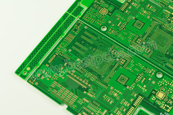
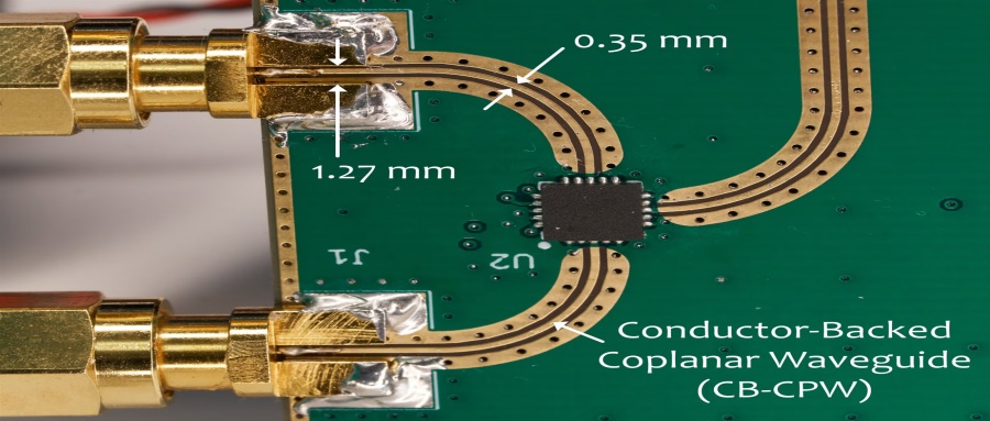
What Is a Coupon in an RF Circuit Board?

A coupon, or test coupon, is a dedicated section on the production panel containing duplicate traces and structures of the actual RF board. It is sacrificial and used for destructive and non-destructive testing to verify the manufacturing process without damaging the functional boards.

  • Impedance Verification:​ Contains microstrip and stripline traces of the same geometry as the design, measured with a Time Domain Reflectometer (TDR) to confirm impedance meets spec.
  • Material & Process Validation:​ Used to test laminate Dk/Df, plating quality, and etch accuracy, ensuring the entire batch meets the required electrical standards.

In a nutshell, the coupon is the quality assurance certificate for an RF PCB, providing empirical data that the board was built to the exact electrical specifications.

Critical Testing Considerations in RF Circuit Board Assembly for Stable RF Performance

RF circuit board assembly​ adds another layer of variables that can degrade performance. Testing must go beyond “opens and shorts.”

  • Pre-Assembly Inspection:​ Verify bare board impedance and loss using coupon data. Inspect for surface defects on pads.
  • Solder Paste & Reflow Profiling:​ Use low-residue, no-clean pastes. Precisely control reflow profiles to prevent thermal shock to sensitive RF components and laminates.
  • Post-Assembly RF Testing:​ Perform functional RF testing (e.g., gain, noise figure, output power) using a test fixture that connects to the board’s RF ports. This is the ultimate validation.
  • Environmental Stress Screening (ESS):​ For critical applications, subject assemblies to thermal cycling and vibration to screen for infant mortality and workmanship issues.
  • Conformal Coating Validation:​ If used, ensure the coating material is RF-transparent (low Dk/Df) and uniformly applied to prevent impedance shifts.

In closing, RF assembly testing is performance-centric, focusing on ensuring the assembled module meets its S-parameter and functional specifications in real-world conditions.

How Engineers Identify, Shield, and Optimize RF Paths on RF Printed Circuit Boards in Complex Systems?

In complex systems, managing RF printed circuit boards​ involves isolating sensitive RF paths from noisy digital domains.

  • Identification & Partitioning.​ Use schematic and layout tools to highlight all RF nets. Physically partition the board into distinct RF, analog, and digital sections.
  • Shielding.​ Implement “canyons” of grounded shielding vias (stitched at < λ/20 spacing) between sections. For critical circuits like an RF receiver circuit board​ LNA, use soldered metal shielding cans to create a full Faraday cage.
  • Optimization.
    • Routing:​ Keep RF traces short, direct, and on the top layer adjacent to a ground plane. Avoid crossing plane splits.
    • Grounding:​ Use a solid, unbroken ground plane under RF sections. Employ multiple vias to connect ground pours and component pads to the plane.
    • Filtering:​ Use feedthrough capacitors and π-filters at the power entry points to each section to prevent noise coupling via supply lines.

In essence, effective management of RF paths relies on strategic physical partitioning, robust shielding via fences or cans, and meticulous attention to grounding and routing to preserve signal purity.

What Makes EBest Circuit (Best Technology) the Optimal RF Printed Circuit Boards Supplier?

EBest Circuit (Best Technology) stands out as a premier RF PCB supplier by combining nearly two decades of specialized manufacturing experience with rigorous, data-driven process capabilities. Our optimal service is built on four key pillars:

1. Deep Technical Expertise and Material Mastery

  • Specialized Materials:​ We are experts in processing high-frequency materials essential for RF performance, including Rogers (e.g., RO4003, RO4350B)​ and PTFE (Teflon), as documented in our capabilities.
  • Proven Process Control:​ RF boards require complex copper plating and precise fabrication. Our experienced engineers successfully manage these challenges, ensuring reliable plated through-holes and consistent performance. Our certifications (ISO9001, IATF 16949) underscore our commitment to quality.

2. Advanced and Quantifiable Manufacturing Capabilities

Our technical specifications, validated by our equipment, provide tangible evidence of our ability to meet demanding RF designs:

  • High-Precision Fabrication:​ We achieve fine lines/spaces down to 2.5/2.5 mil​ for inner layers and 3/3 mil​ for outer layers, crucial for controlled impedance and signal integrity.
  • Laser Drilling Technology:​ We support advanced HDI designs with laser-drilled micro-vias as small as 0.07mm.
  • Impedance Control:​ We guarantee tight impedance tolerances of ±5Ω (for values <50Ω) or ±10% (≥50Ω), ensuring your RF circuits perform as designed.
  • Board Size and Thickness:​ We handle a wide range of requirements, from 3x3mm​ prototypes to large-format arrays up to 610x610mm, with board thicknesses from 0.15mm to 10mm.

3. Speed and Flexibility from Prototype to Production

  • Rapid Prototyping:​ We understand the iterative nature of RF design. Our expedited services can ship urgent 1-2 layer RF prototypes within 24 hours, allowing for quick testing and validation.
  • Seamless Scaling:​ With a massive monthly production capacity of 28,900 square meters, we ensure a smooth transition from prototype to mass production without compromising quality or lead times, supported by a 97% on-time delivery rate.

4. True Partnership and Comprehensive Turnkey Solutions

  • Engineering Support:​ We go beyond manufacturing by offering engineering and DFM feedback, acting as an extension of your R&D team to de-risk designs.
  • Full Turnkey Service:​ We provide a complete solution, from PCB fabrication and component sourcing​ to assembly (PCBA)​ and final box build, simplifying your supply chain.

Overall, EBest Circuit (Best Technology) is the optimal partner because we deliver more than just boards; we deliver certified quality, proven technical capability, and a collaborative partnership​ focused on accelerating your RF product’s success.

RF Circuit Board

In conclusion, RF circuit board​ is the foundational platform that determines the ultimate performance and reliability of any wireless or high-speed system. This guide has explored the critical aspects of RF PCBs, from material science and design principles to advanced manufacturing and testing.

Success in this demanding field requires a partner with the right blend of expertise, precision, and speed. BEST Technology is committed to being that partner, providing custom RF circuit board solutions with quick prototypes​ to accelerate your RF circuits Project. For a consultation or quote, please contact our engineering team at sales@bestpcbs.com.

FAQs

How to Identify an RF Antenna on a Circuit Board?

Look for a unique copper trace, often curved, meandered, or forming a patch, typically located on the board’s edge or in a corner. It is usually connected to an RF transceiver chip via a controlled-impedance trace and is isolated from ground pours in its immediate vicinity.

What Is a Radio RF Pass-Through Circuit Board?

It is a specialized board designed solely to route an RF signal from one connector (e.g., on the chassis wall) to another inside an enclosure with minimal loss and reflection. It acts as a high-performance, shielded feedthrough, often using coaxial-like structures within the board.

What Parts of a Circuit Board Confine RF Transmission Signals?

The primary elements are the ground planes​ above and below the signal trace (in stripline) or below it (in microstrip), which create a controlled electromagnetic field. Additionally, shielding via fences​ running alongside the trace form a waveguide-like structure that confines the field and prevents radiation and crosstalk.

Reliable RF Board Solutions with Complex Microwave and RF Designs
Friday, December 12th, 2025

An RF board is a specialized printed circuit board designed to transmit and process radio-frequency signals ranging from 3 kHz to 300 MHz, and in many practical designs extending into the microwave range from 300 MHz up to 300 GHz, where signal integrity, low transmission loss, and precise impedance control are mandatory for reliable operation.

What are the most common obstacles in sourcing and deploying a reliable RF microwave PCB board?

  • Material Missteps: Using standard FR-4 at GHz frequencies causes excessive dielectric loss and unstable thermal performance.
  • DFM Gaps: RF circuit board designs pass simulation but fail in production due to unrealistic tolerances.
  • Inconsistent Fabrication Quality: Poor process control leads to impedance variation, copper roughness, and delamination.
  • Supply Chain Risks: Difficulty sourcing RF boards that consistently meet military or UL/CE compliance.
  • Insufficient Testing: Basic inspections miss critical RF board test issues such as PIM or resonance.

The solution lies in collaborating with a specialist fabricator whose entire process is engineered for high-frequency success.

  • Expert Material Selection: Choose proven RF laminates such as Rogers or Taconic, including metal-backed options when required.
  • Early DFM Collaboration: Involve the fabricator during RF board layout to ensure manufacturable stack-ups and vias.
  • Precision Manufacturing Processes: Apply LDI, plasma desmear, and controlled impedance etching for high-frequency accuracy.
  • Certified Production Lines: Work with suppliers qualified for mil-spec and regulated RF board production.
  • Advanced RF Testing: Verify performance using TDR, S-parameter analysis, and PIM testing for telecom applications.

This article explores the intricate world of RF and microwave PCB design, material science, and manufacturing, providing a roadmap for achieving reliability in the most demanding applications. BEST Technology is a specialized manufacturer of high-precision, high-frequency PCBs. We combine deep material science knowledge with state-of-the-art fabrication and testing facilities to transform complex microwave and RF designs​ into reliable, production-ready hardware. From RF prototype boards​ to high-volume runs, we ensure your board performs as simulated. Pls feel free to contact our experts at sales@bestpcbs.com​ to start your project.

 RF Board

What Is the Definition of an RF Board?

An RF (Radio Frequency) board is a specialized printed circuit board engineered to transmit, route, and process electromagnetic signals in the radio frequency spectrum, generally covering 3 kHz to 300 MHz.
Within this range, signal behavior transitions from low-frequency electrical conduction to wave-dominated propagation, requiring controlled impedance, stable dielectric properties, and careful layout discipline.

When operating above 300 MHz, PCB designs enter the microwave domain, which typically spans 300 MHz to 300 GHz. At these frequencies, an RF board must function as a guided transmission structure rather than a simple interconnect, making dielectric constant (Dk), dissipation factor (Df), copper surface roughness, stack-up symmetry, and grounding strategy critical to performance.

Unlike standard digital PCBs, RF and microwave boards are designed around signal integrity, insertion loss, phase stability, and electromagnetic compatibility, ensuring predictable behavior across the intended frequency band and operating environment.

 RF Board

Why Microwave Systems Rely on Specialized Microwave PCBs Instead of Standard FR-4 Boards?

At microwave frequencies, the electrical properties of the PCB substrate become the dominant factor in performance. Standard FR-4 is unsuitable due to:

  • High Dielectric Loss (Df):​ Absorbs signal energy, converting it to heat and severely attenuating the signal.
  • Inconsistent Dielectric Constant (Dk):​ Varies with frequency and lot-to-lot, making stable impedance matching impossible.
  • High Moisture Absorption:​ Changes electrical properties and can lead to delamination.
  • Poor Thermal Conductivity:​ Inefficient for heat dissipation from active RF power amplifier​ components.

Specialized microwave PCBs​ use engineered laminates (e.g., PTFE-based ceramics, hydrocarbon ceramics) that offer low loss, stable Dk, low moisture absorption, and often better thermal performance, which is essential for reliable RF circuit board​ operation.

What Materials and Stackups Are Best Suited for an RF Circuit Board Operating at GHz Frequencies?

Material selection is the first critical decision for a successful RF PCB.

Material TypeTypical BrandsKey PropertiesBest For
PTFE/ CeramicRogers RO4000®, Taconic RF-35Low loss, stable Dk, good performanceMulti-layer boards, digital analog integration
Pure PTFERogers RT/duroid®Ultra-low loss, excellent electrical stabilityCritical RF amplifier board, aerospace
Hydrocarbon CeramicRogers RO3000®Low loss, good thermal conductivityMetal core boards​ for high power
Thermoset HydrocarbonIsola IS680-350Cost-effective, lower loss than FR-4Consumer RF module board​

A optimal RF board​ stackup for GHz frequencies should:

  • Use a low-loss core material for RF layers.
  • Implement a symmetrical stackup to prevent warpage.
  • Minimize the distance between RF signal and reference planes to reduce radiation.
  • Use multiple ground vias (stitching) around RF lines to suppress cavity resonances.
  • Consider hybrid stackups (e.g., FR-4 for digital, Rogers for RF) for cost-sensitive, mixed-signal designs.

What Is RF Circuit Board Design?

RF circuit board design​ is the discipline of laying out a PCB to effectively manage high-frequency electromagnetic waves. It transcends simple connectivity, focusing on controlling the behavior of signals as they travel along transmission lines. Core principles include:

  • Controlled Impedance:​ Ensuring signal traces have a consistent characteristic impedance (e.g., 50Ω) to prevent reflections.
  • Transmission Line Theory:​ Using microstrip or stripline geometries rather than simple “wires.”
  • Minimizing Discontinuities:​ Carefully managing bends, vias, and component pads to avoid parasitic inductance/capacitance.
  • Isolation and Shielding:​ Strategic use of grounding, board level EMI RF shields, and spacing to prevent crosstalk and radiation.
  • Thermal Management:​ Providing adequate heat sinking for active components, often integrated into the RF board layout.

What Is the Application of RF Circuit Board?

RF circuit boards​ are the enabling technology for wireless connectivity and signal processing across industries.

  • Telecommunications:​ 5G/6G base stations, satellite comms equipment, and microwave backhaul links.
  • Aerospace & Defense:​ Radar systems, electronic warfare (EW), and avionics requiring suppliers for military specs.
  • Automotive:​ Advanced driver-assistance systems (ADAS), vehicle-to-everything (V2X), and GPS.
  • Medical:​ MRI machines, therapeutic and diagnostic equipment, and wireless monitoring devices.
  • Consumer Electronics:​ Smartphones, Wi-Fi routers, and gaming consoles (e.g., xbox one RF board​ replacements).

Best HDI PCB Manufacturers for RF and Microwave Circuit Boards

Based on 2024–2025 industry data and global market research, the following companies stand out as the world’s leading HDI (High-Density Interconnect) PCB manufacturers for RF (Radio Frequency) and Microwave applications.
These manufacturers demonstrate proven capabilities in ultra-fine line processing, controlled impedance, high-layer HDI builds, and maintain robust certification systems tailored to high-frequency and high-reliability sectors.

🏆 Overall Market Leader

TTM Technologies | United States
Global HDI Market Leader for RF and Microwave Applications

  • TTM Technologies is one of the world’s largest HDI PCB manufacturers, widely recognized for its advanced RF and microwave capabilities across aerospace, defense, telecommunications, and automotive electronics. Its long-term investment in signal integrity engineering and high-layer HDI platforms positions it as a benchmark supplier for mission-critical RF designs.

🇨🇳 China Market Leader

EBest Circuit (Best Technology) | China
Core Supplier for AI Servers and 5G Infrastructure

  • EBest Circuit (Best Technology) plays a dominant role in AI computing infrastructure and advanced communication systems. It is a key PCB supplier for autonomous driving platforms and high-performance computing, with strong HDI and RF manufacturing depth supporting large-scale production.

Top HDI PCB Suppliers

Company NameHeadquartersBoard Type FocusKey Certifications
TTM TechnologiesUSARF / Microwave / Aerospace, ultra-fine lines, high-layer countISO 9001, AS9100, Nadcap, IPC-6012 Class 3
AT&SAustriaAutomotive HDI / RF, sequential lamination, fine trace/spaceIATF 16949, ISO 9001, ISO 14001, AS/EN 9100
UnimicronTaiwanMobile RF / IC Substrate, microvias, stacked viasISO 9001, UL, ISO 14001, IATF 16949
CompeqTaiwanRF / High-Frequency, telecom infrastructure, mobile devicesISO 9001, ISO 14001, UL, IATF 16949
Meiko ElectronicsJapanPrecision HDI / RF, high-reliability manufacturingISO 9001, ISO 14001, UL

Note: Manufacturer selection is based on Prismark market data and a combined evaluation of RF/microwave process barriers, certification depth, and market share.

TTM Technologies (USA)

RF and Microwave Expertise
TTM demonstrates exceptional process maturity in millimeter-wave frequencies and high-frequency signal integrity control, making it a preferred supplier for aerospace and defense RF platforms.

Certification Strength
The company holds Nadcap accreditation, a critical aerospace qualification that many general PCB manufacturers cannot meet, reinforcing its position in high-reliability markets.

AT&S (Austria)

Automotive RF Leadership
AT&S excels in ADAS, automotive radar, and electric vehicle RF systems, where long-term reliability and thermal stability are mandatory.

Quality and Sustainability
Its operations emphasize renewable energy usage and strict compliance with IATF 16949, aligning with global automotive OEM requirements.

Unimicron (Taiwan)

Miniaturization Capability
With trace and space down to 2/2 μm, Unimicron is well-suited for compact, highly integrated RF modules used in smartphones and wireless devices.

Advanced Interconnect Technology
Its strength in ALIVH (Any-Layer Interstitial Via Hole) technology supports complex RF stackups and dense interconnections.

Market Landscape and Industry Trends

Estimated Global HDI Market Share

  • Compeq: 11%
  • Unimicron: 11%
  • TTM Technologies: 10%
  • AT&S: 7.7%
  • Other manufacturers: 60%

Data source: Prismark 2024 global HDI market report. The listed companies represent the core share holders in RF and microwave HDI manufacturing.

Practical Selection Recommendations

When selecting an HDI PCB manufacturer for RF and microwave applications, consider the following guidance:

  • Aerospace or military-grade systems
    Prioritize TTM Technologies or AT&S, as both maintain AS9100 and Nadcap certifications.
  • Automotive radar and ADAS platforms
    AT&S offers the most comprehensive automotive-focused RF certification portfolio.
  • Consumer electronics and 5G infrastructure
    Unimicron or Compeq provide high-precision RF manufacturing with competitive cost structures.
  • Ultra-thin or high-layer RF designs
    Meiko Electronics delivers unique advantages in precision HDI and long-term manufacturing stability.

Top Companies for RF Microwave PCB and Metal Core Boards

Based on the latest industry data and search insights, the following five companies are widely recognized as global leaders in RF/Microwave and Metal Core PCB manufacturing.
Their market position is driven by strong capabilities in high-frequency material processing, precision fabrication, and strict certification systems, enabling them to serve demanding applications across aerospace, defense, telecom, automotive, and high-power electronics.

🌍 Global High-End Manufacturers

  • Advanced Circuitry International (ACI)

United States | RF/Microwave Specialist

Core Strengths
ACI focuses exclusively on RF and microwave antenna PCB manufacturing, with more than 30 years of industry experience supporting high-reliability programs.

RF Capabilities
The company is well known for large-format PCB fabrication, blind and buried vias, and advanced Ohmegaply™ hybrid constructions, enabling excellent impedance stability and thermal control.

Material Support
Extensive experience with Rogers, Taconic, Arlon, and other premium RF laminates.

Certifications
ISO 9001, AS9100D, ITAR registered.

  • Teledyne Labtech

UK / USA | Military and High-Reliability Applications

Core Strengths
Teledyne Labtech delivers solutions for military and harsh commercial environments, including advanced technologies such as embedded graphite layers for thermal management.

RF Capabilities
Full-size PCB manufacturing, antenna fabrication, and integrated thermal control solutions for RF and microwave systems.

Certifications
ISO 9001, ISO 14001, JOSCAR.

🇨🇳 Asia-Based Supply Chain Leaders

  • EBest Circuit (Best Technology)

China | Comprehensive PCB and Assembly Services

Core Strengths
EBest Circuit (Best Technology) provides one-stop manufacturing services, covering both metal core PCB fabrication and complete PCBA assembly.

Metal Core Capability
Manufactures single-layer and multilayer aluminum- and copper-based metal core boards, suitable for power electronics and thermal-intensive designs.

Certifications
UL, IATF 16949, ISO 9001, ISO 13485, AS9100D CE, RoHS.

Key Capability Overview

Company NameBoard TypeKey Certifications
Advanced Circuitry InternationalRF/Microwave, AntennaISO 9001, AS9100D, ITAR
Teledyne LabtechRF/Microwave, MilitaryISO 9001, ISO 14001, JOSCAR
EBest Circuit (Best Technology)Metal Core, Flexible, Rigid PCB, RF/MicrowaveISO 9001, ISO 13485, IATF 16949, AS9100D, UL, REACH, and RoHS.

How to Select the Right RF Microwave PCB Board Supplier for High-Reliability Industries

Choosing a RF microwave pcb board supplier​ for medical, aerospace, or defense applications requires due diligence.

  • Audit Quality Systems:​ Review their AS9100 or ISO13485 certifications and audit reports.
  • Evaluate Technical Support:​ Assess their engineers’ ability to discuss RF board design guidelines​ and material trade-offs.
  • Inspect Testing Capabilities:​ Ensure they have the required RF board test​ equipment (e.g., TDR, network analyzer, flying probe).
  • Review Documentation:​ Request examples of travel coupons, test reports, and material certifications.
  • Check Industry References:​ Ask for case studies or contacts in your specific field (e.g., medical devices, telecom networks).

How Do You Streamline RF Board Installation for High-Reliability Designs?

Streamlining RF board installation​ prevents field failures. Key practices include:

  • Clear Mechanical Documentation:​ Provide detailed drawings showing keep-out areas, shield placement, and torque specs for board to board RF connectors.
  • Integrated Alignment Features:​ Design in tooling holes, dowel pins, or guides for error-free assembly.
  • Standardized Connectorization:​ Use common, reliable RF board to board connector​ types to simplify cabling.
  • Comprehensive Assembly Instructions:​ Create visual work instructions covering handling, ESD, soldering, and cleaning.
  • On-Board Test Points:​ Include accessible coaxial test points for validation during system integration.

What Testing and Validation Methods Are Required for Reliable RF Board Test Results?

A robust RF board test​ protocol is essential for reliability.

  • Automated Optical Inspection (AOI):​ Checks for surface defects and solder issues.
  • Controlled Impedance Testing:​ Uses a Time Domain Reflectometer (TDR) to verify trace impedance meets design specs (e.g., 50Ω ±10%).
  • Network Analysis:​ Measures S-parameters (S11, S21) to validate insertion loss, return loss, and isolation across the operational bandwidth.
  • High-Potential (HiPot) Testing:​ Ensures dielectric strength and electrical isolation.
  • Specialized Tests:​ May include passive intermodulation (PIM) testing for telecom, or thermal cycling for environmental robustness.

Where to Get RF Microwave PCB Boards Metal-Backed?

Metal-backed PCBs​ (also called metal-clad or insulated metal substrates) are ideal for high-power RF applications. They are available from specialized fabricators who:

  • Offer Various Metals:​ Typically aluminum (for cost and weight) or copper (for best thermal performance).
  • Handle Dielectric Bonding:​ Expertly laminate a thin, thermally conductive but electrically insulating dielectric layer to the metal base.
  • Manage CTE Mismatch:​ Use processes that prevent warping or delamination during thermal cycling.
  • Provide Secondary Operations:​ Offer machining, tapping, and anodizing of the metal base as part of the service.

Why EBest Circuit (Best Technology) Is the Best Partner for RF Boards Fabrication?

EBest Circuit (Best Technology) distinguishes itself as a leader in the fabrication of complex Radio Frequency (RF) and Microwave printed circuit boards. Our expertise is demonstrated through hard process data, advanced engineering capabilities, and full control over the manufacturing value chain.

1. Mastery of High-Frequency Materials

We specialize in processing a wide range of advanced substrates critical for RF performance, ensuring optimal signal integrity and controlled dielectric properties.

  • Material Portfolio:​ Expertise in Rogers (e.g., 4350B, 4003), PTFE (Taconic, Arlon), and ceramic-filled materials (M-series).
  • Layer Count:​ Capable of manufacturing highly complex multilayer boards up to 50 layers​ (standard), with advanced capabilities for up to 100 layers​ (upon review).

2. Precision Engineering for Critical RF Parameters

Our processes are calibrated to meet the tight tolerances required for high-frequency applications.

  • Fine Lines/Spacing:​ Standard outer layer trace/space of 3.5/4 mil​ for 1oz copper, with advanced capabilities down to 3/3 mil.
  • Micro-Vias & Drilling:​ Laser drilling for HDI designs down to 0.07mm. Exceptional mechanical drill hole position accuracy of ±0.05mm.
  • Controlled Impedance:​ Industry-leading impedance control with tolerances as tight as ±4Ω (for impedances <50Ω)​ or ±6% (for impedances ≥50Ω).
  • RF-Suitable Surface Finishes:​ Including ENIG​ (Nickel: 3-8µm, Gold: 0.025-0.125µm), Immersion Silver, and OSP.

3. Uncompromising Quality and Reliability

We ensure board performance and reliability through stringent process controls.

  • Layer-to-Layer Registration:​ Advanced registration control of ≤0.13mm.
  • Solder Mask Alignment:​ Precision alignment tolerance of ±0.05mm.
  • Board Flatness:​ Superior warpage control, with a capability of 0.005.

To sum up, EBest Circuit (Best Technology) provides a proven foundation for your most demanding RF applications, backed by concrete data in high-frequency material processing (Rogers/PTFE), complex stack-ups (to 50L), fine features (3/3 mil), tight impedance control (±4Ω), and precision drilling (0.07mm laser vias).

All in all, RF Boards​ are the precision-engineered backbone of modern wireless systems, where every micron and material property dictates performance. This guide has navigated the critical aspects of RF and microwave PCB design, manufacturing, and validation, emphasizing the partnership required to achieve reliability.

For projects where performance cannot be compromised, partnering with a specialist is paramount. BEST Technology provides that essential edge, combining deep technical expertise with manufacturing excellence to deliver robust, high-yield RF solutions. Reach out to start a conversation about your most challenging high-frequency designs via sales@bestpcbs.com.

 RF Board

FAQs

What is the function of an RF prototype board?

  • An RF prototype board​ serves to physically validate the RF circuit board design, material selection, and manufacturing processes before committing to full-scale production. It allows engineers to test real-world performance, debug issues, and refine the layout, ensuring the final product meets all electrical and mechanical specifications.

What are the common pitfalls in RF board installation?

  • Common pitfalls in RF board installation​ include:
    1) Using excessive torque on connectors, damaging the PCB pads;
    2) Improper grounding of board level EMI RF shields, creating unintended antennas;
    3) Pinching or stressing coaxial cables, altering their impedance;
    4) Applying incorrect soldering profiles, damaging heat-sensitive laminates; and
    5) Failing to clean flux residues, which can become conductive at RF frequencies.

How do you optimize designs for double-sided RF board assemblies?

To optimize designs for double-sided RF board assemblies:

  • 1) Dedicate one side primarily as a continuous, unbroken ground plane.
  • 2) Route sensitive RF traces on one side only, using the other side for DC/power and low-speed signals.
  • 3) Use abundant ground vias to stitch the top and bottom ground planes together, minimizing ground loop impedance.
  • 4) Place components strategically to avoid interference, and
  • 5) carefully model and place vias that must transition signals between layers to minimize their discontinuity.

Premium HDI RF Board for Reliable High-Frequency Designs
Monday, December 8th, 2025

An HDI RF Board is a sophisticated printed circuit board that merges High-Density Interconnect technology with specialized materials and design rules to excel in radio frequency applications. Pushing the limits of modern wireless, radar, and sensing systems demands circuits that are faster, smaller, and more reliable than ever. This article provides a comprehensive guide to understanding HDI RF boards, their advantages for high-frequency designs, key structural elements, cost considerations, comparisons with other substrates, and guidance on selecting a reliable HDI PCB manufacturer.

Are your current PCB solutions holding back your next-generation RF design? You might be facing these common challenges:

  • Signal Degradation at High Frequencies:​ Standard PCB constructions struggle with significant signal loss, crosstalk, and impedance discontinuities, crippling the performance of sensitive RF and microwave circuits.
  • Size and Weight Constraints:​ Achieving complex functionality often means larger, multilayer boards that contradict the miniaturization goals of modern portable and aerospace electronics.
  • Thermal Management Headaches:​ Dense component placement and high-power RF sections generate concentrated heat that standard boards cannot effectively dissipate, leading to reliability risks.
  • Prototyping and Yield Frustrations:​ Complex RF designs often require multiple expensive prototype iterations, and manufacturing defects in fine features can lead to poor yield and project delays.
  • Supply Chain and Expertise Gaps:​ Finding a manufacturer with both advanced HDI technology in PCB​ fabrication and deep RF/microwave​ design support is difficult, leading to communication breakdowns and suboptimal results.

The solution lies in partnering with a specialist who masters the fusion of HDI fabrication and RF principles. At BEST Technology, we engineer Premium HDI RF Boards​ specifically to overcome these hurdles.

  • Superior Signal Integrity:​ We utilize advanced HDI layer​ stacking, low-loss materials, and precise impedance control to ensure clean, high-fidelity signal transmission for your RF and microwave circuit boards.
  • Enabled Miniaturization:​ Our expertise in microvias and fine-line patterning packs more functionality into a smaller footprint, crucial for compact HDI Electronics​ and antenna systems.
  • Enhanced Thermal & Mechanical Reliability:​ We integrate thermal management strategies and robust stack-up designs from the start, ensuring your board remains stable and reliable under operational stress.
  • DFM-Driven Process & High Yield:​ Our design-for-manufacturability review and controlled processes reduce prototyping cycles and ensure high production yield, even for complex designs like HF RFID antenna​ modules.
  • One-Stop Expert Partnership:​ As a leading HDI RF Board manufacturer, EBest Circuit (Best Technology) provides end-to-end support—from material selection and design review to advanced fabrication and testing—simplifying your supply chain.

BEST Technology is a premier specialist in manufacturing advanced printed circuit boards, with over 19 years of expertise in HDI PCB​ and high-frequency solutions. We combine state-of-the-art production facilities with profound technical knowledge to serve clients in telecommunications, aerospace, defense, and medical industries. We are not just a HDI PCB manufacturer; we are your technical partner in realizing cutting-edge HDI RF​ designs and solutions. For inquiries, pls feel free to contact us at sales@bestpcbs.com.

HDI RF Board

What Is an HDI RF Board?

At its core, an HDI RF Board is defined by the application of High-Density Interconnect (HDI) methodologies to boards operating at radio frequencies. To understand the HDI PCB definition, it is a board with a higher wiring density per unit area than conventional PCBs, achieved through features like microvias (laser-drilled), fine lines and spaces, and sequential lamination. When this is applied to RF designs, it involves using specialized low-loss laminate materials (like Rogers, Taconic) alongside these HDI techniques.

How HDI RF Circuit Board Differs from Standard High-Frequency Designs? Here’s how it differs from standard RF boards:

  • Interconnect Density:​ Standard RF boards often use larger through-hole vias, limiting routing space. HDI RF boards employ microvias (often blind and buried), allowing escape routing from dense RF ICs (like BGAs) and more efficient layer transitions.
  • Material Integration:​ While both may use similar high-frequency laminates, HDI RF boards require materials that are also compatible with the multiple lamination cycles and fine-feature etching of HDI processes.
  • Design for Performance and Size:​ A standard design might increase board size to accommodate components and routing. An HDI RF design optimizes both electrical performance (shorter, controlled paths) and physical size simultaneously.
  • Manufacturing Complexity:​ The fabrication of HDI RF boards is significantly more complex, requiring precise control over dielectric thickness, via formation, and copper profiling to maintain consistent RF characteristics.

In summary, an HDI RF board is the strategic convergence of miniaturization technology (HDI) and high-frequency engineering, creating a platform that is superior for modern, compact, and high-performance wireless devices.

HDI RF Board

Why HDI Technology in PCB Matters for RF Performance?

The role of HDI technology in PCB​ fabrication is transformative for RF applications. It directly addresses the critical demands of high-frequency circuits.

  • Minimized Signal Path Length:​ Shorter traces between components, enabled by dense interconnects, reduce signal delay, propagation loss, and the chance of picking up noise.
  • Improved Impedance Control & Signal Integrity:​ The fine-line capabilities of HDI allow for precise control over trace width and spacing, which is paramount for maintaining consistent characteristic impedance (e.g., 50Ω) across the board, minimizing reflections.
  • Reduced Parasitic Effects:​ Microvias have lower parasitic capacitance and inductance compared to traditional through-hole vias. This is crucial at GHz frequencies, where via stubs can act as antennas or cause resonances.
  • Enhanced Grounding and Shielding:​ Multiple buried vias can create a dense via fence or a coaxial-like shielding structure around sensitive RF lines, effectively containing electromagnetic interference (EMI) and crosstalk.
  • Facilitation of Advanced Packaging:​ HDI is essential for integrating embedded passive components (resistors, capacitors) and for fan-out routing from advanced semiconductor packages, keeping the entire RF front-end compact and efficient.

For RF performance, HDI is not just about making the board smaller; it’s about making it electrically superior by reducing negative effects intrinsic to larger, conventional geometries.

Key Structure and HDI Layer Configurations Used in Advanced RF Modules and Antenna Systems

The architecture of an HDI RF board is its blueprint for success. The HDI layer​ build-up is carefully planned to meet electrical and mechanical goals.

  • Standard “1+N+1” to “Any Layer” Build-Ups:​ Simple HDI starts with “1+N+1” (one HDI layer on each side of a core). Advanced RF modules may use “2+N+2” or “any layer” HDI, where almost every layer can be connected with microvias, offering maximum design flexibility for complex HDI Electronics.
  • Hybrid Material Stack-ups:​ A common configuration uses a high-performance, low-loss RF laminate (e.g., Rogers 4350B) for critical signal layers, bonded with standard FR-4 prepreg for other layers. This optimizes cost and performance.
  • Buried and Blind Via Structures:​ Critical RF lines often reside on outer layers for best performance. Blind vias connect surface layers to adjacent inner layers without going through the entire board, preserving space and reducing stub length.
  • Via-in-Pad and Filled Vias:​ To further miniaturize, vias are placed directly in component pads. These are plated and filled with conductive or non-conductive material, creating a flat surface for soldering and excellent thermal conduction for components like power amplifiers.
  • Shielding Cavities and Antenna Structures:​ HDI processes can create milled cavities for shielding cans or precise, multi-layer antenna structures like patch antennas for HF RFID antenna​ systems, all integrated within the board itself.

This sophisticated layering is what allows a single, compact HDI RF Board​ to function as an entire RF subsystem.

What is HDI RF Board Price?

The HDI RF board price​ is not a fixed number but a variable determined by a confluence of technical factors. Understanding these helps in budgeting and design optimization.

  • Board Complexity:​ This is the primary driver. More sequential lamination cycles, a higher count of laser-drilled microvias, and “any layer” capability increase cost significantly.
  • Material Selection:​ High-frequency laminates (Rogers, Taconic, etc.) are far more expensive than standard FR-4. The percentage of these materials in the hybrid stack-up directly impacts the raw board cost.
  • Layer Count and Size:​ More layers and a larger board area naturally increase material and processing time. HDI allows for smaller sizes, which can offset the cost of increased layer count.
  • Specialized Processes:​ Costs for via-in-pad, filled vias, tight impedance control tolerances (e.g., ±5%), and advanced surface finishes (ENEPIG) add to the final price.
  • Order Volume and Turnaround Time:​ Prototype quantities have a higher cost per unit. Production volumes bring economies of scale. Expedited fabrication also carries a premium.

As a rough guideline, expect an HDI RF board to cost 2 to 5 times more​ than a standard FR-4 PCB with the same dimensions and layer count, primarily due to materials and process complexity. The investment, however, is justified by the unparalleled performance and integration it enables.

Comparing HDI Electronics with Flex PCB, LED PCB, and Other Specialized Substrates for RF Applications

Choosing the right substrate is critical. Here’s how HDI Electronics​ compare:

  • HDI RF Board vs. Flex PCB:​ Flex boards offer dynamic bending and space savings in assemblies. However, for core RF circuitry, standard flex materials often have higher loss tangents. HDI rigid boards provide better rigidity for component support, superior thermal management, and wider availability of ultra-low-loss laminate options. They are often used together (Rigid-Flex) where HDI areas handle the core RF processing.
  • HDI RF Board vs. Standard LED PCB:​ A typical LED PCB​ prioritizes high thermal conductivity (using metal core like Aluminum) and simple circuitry to drive LEDs. An HDI RF board is focused on signal integrity at high frequencies, using different materials and complex, controlled-impedance routing. Their purposes are distinct.
  • HDI RF Board vs. Standard FR-4 Multilayer:​ Standard multilayer boards lack the fine features and low-loss materials. They are unsuitable for high-frequency performance but are cost-effective for digital and low-frequency analog sections. HDI RF is the specialized choice for the RF front-end.
  • HDI RF Board vs. Pure Ceramic Substrate (e.g., Alumina, LTCC):Ceramic offers excellent thermal performance and very fine features but at a very high cost and limited size. HDI RF on organic laminates provides a better balance of performance, size, design flexibility, and cost for most RF applications below the millimeter-wave extreme.

In essence, for the heart of a high-frequency system—where signal integrity, miniaturization, and integration are non-negotiable—the Premium HDI RF Board​ is the unmatched solution.

How HF RFID Antenna, RFI Board, and RDI Board Designs Benefit from HDI Technology?

These specialized applications gain distinct advantages:

  • HF RFID Antenna:​ It is short for High Frequency Radio Frequency Identification Antenna. HF RFID antenna​ coils often require precise, multi-turn patterns. HDI technology allows these coils to be fabricated with extreme accuracy as embedded planar structures within the board layers, improving reliability and enabling integration with the control chip in a single, slim package.
    Application: Operating at the 13.56 MHz HF band, these HDI-enabled antenna inlays or modules are critical for contactless payment systems (e.g., credit cards, mobile wallets), secure access control badges, library item tracking, and high-security document authentication.
  • RFI (Radio Frequency Interference) Board:​ Boards designed to mitigate RFI​ need excellent shielding. HDI allows for the easy creation of dense ground via fences and shielded cavities between noisy and sensitive sections directly within the board structure, providing superior isolation compared to external shields.
    Application: Crucial for applications across a wide frequency spectrum, these boards are used in sensitive medical imaging equipment (MRI), high-density telecom infrastructure, aerospace avionics, and advanced test & measurement instruments to prevent signal degradation and ensure regulatory EMI/EMC compliance.
  • RDI (Research, Development, and Innovation) Boards:Prototype and RDI board​ projects for cutting-edge technology benefit immensely from HDI’s flexibility. It allows researchers to pack sensors, RF components, and digital processors into a small form factor for proof-of-concept devices, accelerating innovation cycles.
    Application: :​ Used in prototyping next-generation IoT devices, millimeter-wave (mmWave) communication systems (e.g., 5G/6G fronthaul), phased array radar elements, and quantum computing interfaces, where form factor, signal integrity, and rapid design iteration are paramount.

In all cases, HDI provides the design freedom and performance consistency needed to turn advanced concepts into reliable, manufacturable products.

How to Select Reliable HDI RF Board Manufacturers?

Choosing the right partner is as important as the design itself. Look for these traits in HDI RF board manufacturers:

  • Proven Technical Expertise:​ They must demonstrate a deep understanding of both HDI processes and RF principles (impedance, loss, materials).
  • Advanced Manufacturing Capability:​ Verify they have laser drilling, precision lamination, and electrical testing equipment (like network analyzers) specifically for RF parameters.
  • Material Partnerships:​ Access to a wide range of certified high-frequency laminates from leading suppliers is essential.
  • Design Support Services:​ The best manufacturers offer upfront engineering support, including stack-up design, simulation assistance, and thorough DFM analysis.
  • Quality and Certifications:​ Look for relevant industry certifications (ISO, IATF 16949, AS9100 for aerospace) and a robust quality management system.
HDI RF Board

Why Choose BEST Technology as One of Your Best HDI PCB Manufacturers for RF and Microwave Circuit Boards?

BEST Technology stands out by fulfilling all the above criteria and more. We specialize in the niche intersection of HDI and high-frequency, offering:

  • Dual Expertise:​ Our engineers are fluent in the language of both advanced fabrication and RF design.
  • State-of-the-Art Facility:​ Equipped with specialized lines for handling low-loss materials and achieving tight tolerances.
  • End-to-End Partnership:​ We collaborate from the early design stage through prototyping to volume production, ensuring your RF and microwave circuit boards​ are not only designed well but are also optimized for manufacturability and yield.
  • Commitment to Reliability:​ Every Premium HDI RF Board​ we build undergoes rigorous testing to meet the stringent requirements of high-reliability applications. And our PCB and SMT factory is fully compatible with ISO 9001, ISO 13485, IATF 16949, AS9100D, UL, REACH, and RoHS.
  • Short Lead Times: We operate dedicated, streamlined production lines and maintain strategic raw material partnerships. This optimized workflow, combined with our deep process expertise, allows us to offer industry-leading turnaround times for both complex prototypes and volume production, enabling you to accelerate your product development and meet critical market windows without compromising on quality.
HDI RF Board

All in all, an HDI RF Board​ represents the pinnacle of integration for high-frequency electronics, combining the miniaturization power of HDI with the performance demands of RF circuits. This guide has explored its HDI PCB definition, benefits, structures, costs, and ideal applications to help you leverage this advanced technology for your most demanding projects.

Success in this field requires a manufacturer that is more than a fabrication house; it requires a technical co-innovator. BEST Technology brings nearly two decades of specialized HDI RF circuit board experience, cutting-edge capabilities, and a partnership-driven approach to every HDI device project. Pls feel free to contact us for a consultation or quote via sales@bestpcbs.com

FAQs

Q: What is the difference between HDI PCB and regular PCB?

  • A: The main differences are density and construction. HDI PCBs use microvias (typically <150µm), finer traces/spaces, and often sequential build-up to achieve much higher interconnection density in a smaller area compared to regular PCBs that rely on larger through-hole vias and simpler lamination.

Q: What are the benefits of HDI PCB?

  • A: Key benefits include significant size and weight reduction, improved electrical performance (faster signals, less noise), enhanced reliability (fewer mechanical interconnections), and the ability to accommodate advanced, high-pin-count components like BGAs.

Q: What are the 4 tiers of HDI?

A: HDI complexity is often categorized into tiers:

  • Tier 1:​ 1+N+1 (Microvias on one side of the core).
  • Tier 2:​ 2+N+2 (Microvias on both sides, potentially with stacked vias).
  • Tier 3:​ 3+N+3 (Multiple layers of stacked microvias).
  • Tier 4 & Above:​ Also called “Any Layer” HDI, where microvias can connect any two adjacent layers throughout the board stack-up.

Q: What is the process of HDI PCB fabrication?

  • A: It involves sequential lamination cycles. Key steps include: imaging and etching of fine inner layers, laser drilling of microvias, via metallization (plating), layer alignment and bonding (lamination), and repeat. This differs from standard PCB fab which often uses a single lamination of all layers followed by mechanical drilling of through-holes.

Q: What is an HDI device?

  • A: In the context of PCBs, an “HDI device” typically refers to the final electronic product or module that is enabled by or built upon an HDI printed circuit board, such as a smartphone, a satellite communication module, or a medical imaging device.