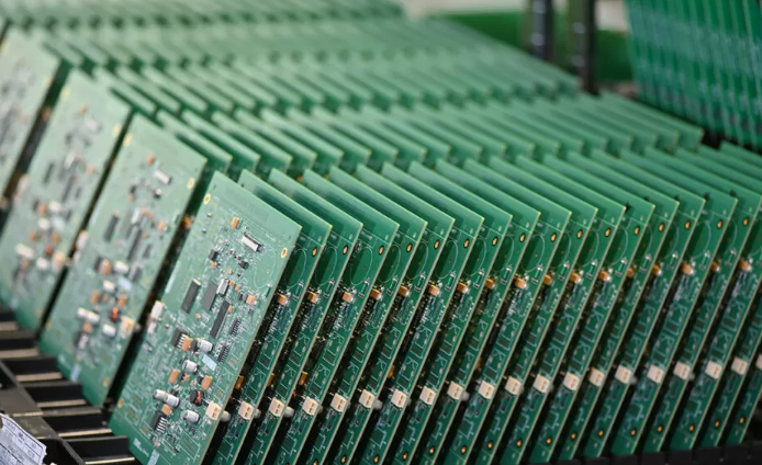
Understanding active and passive components is essential for designing reliable circuits. Whether you work in consumer electronics, automotive, or industrial systems, mastering active and passive components helps you choose the right parts for performance, cost, and longevity. This guide breaks down everything you need to know about active and passive components, from definitions to real-world applications.
What Are Active Components in Electronics? Definition & Examples
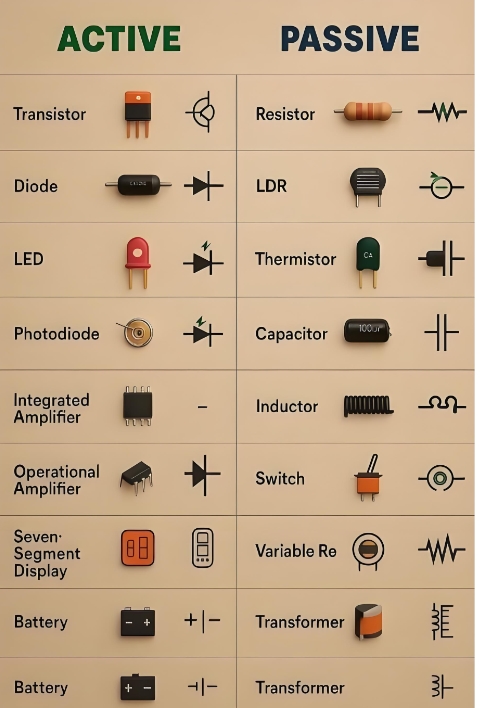
Active components need an external power source to function. They control or amplify electrical signals, making them critical for circuit performance.
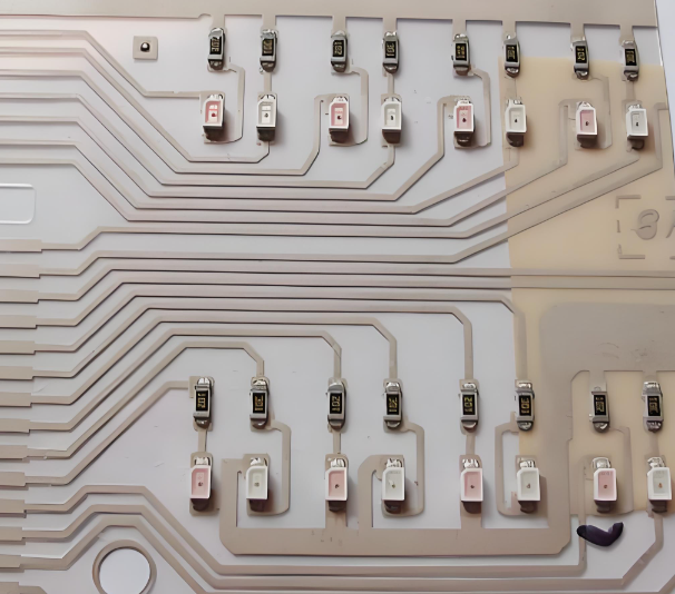
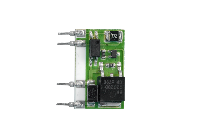
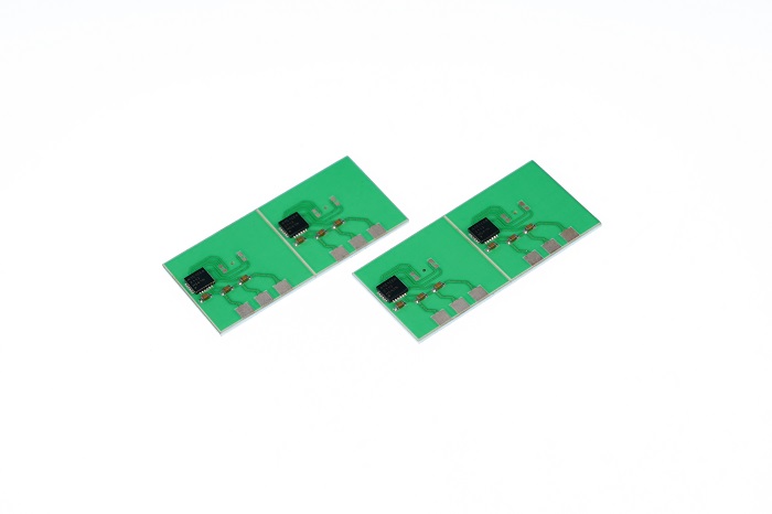
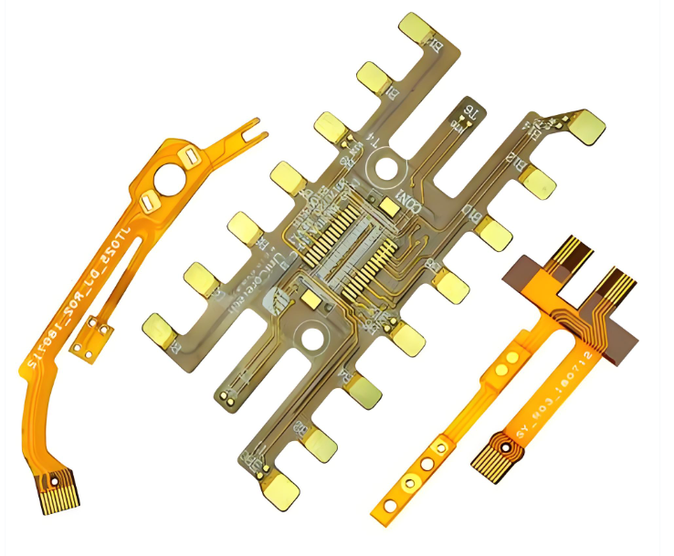
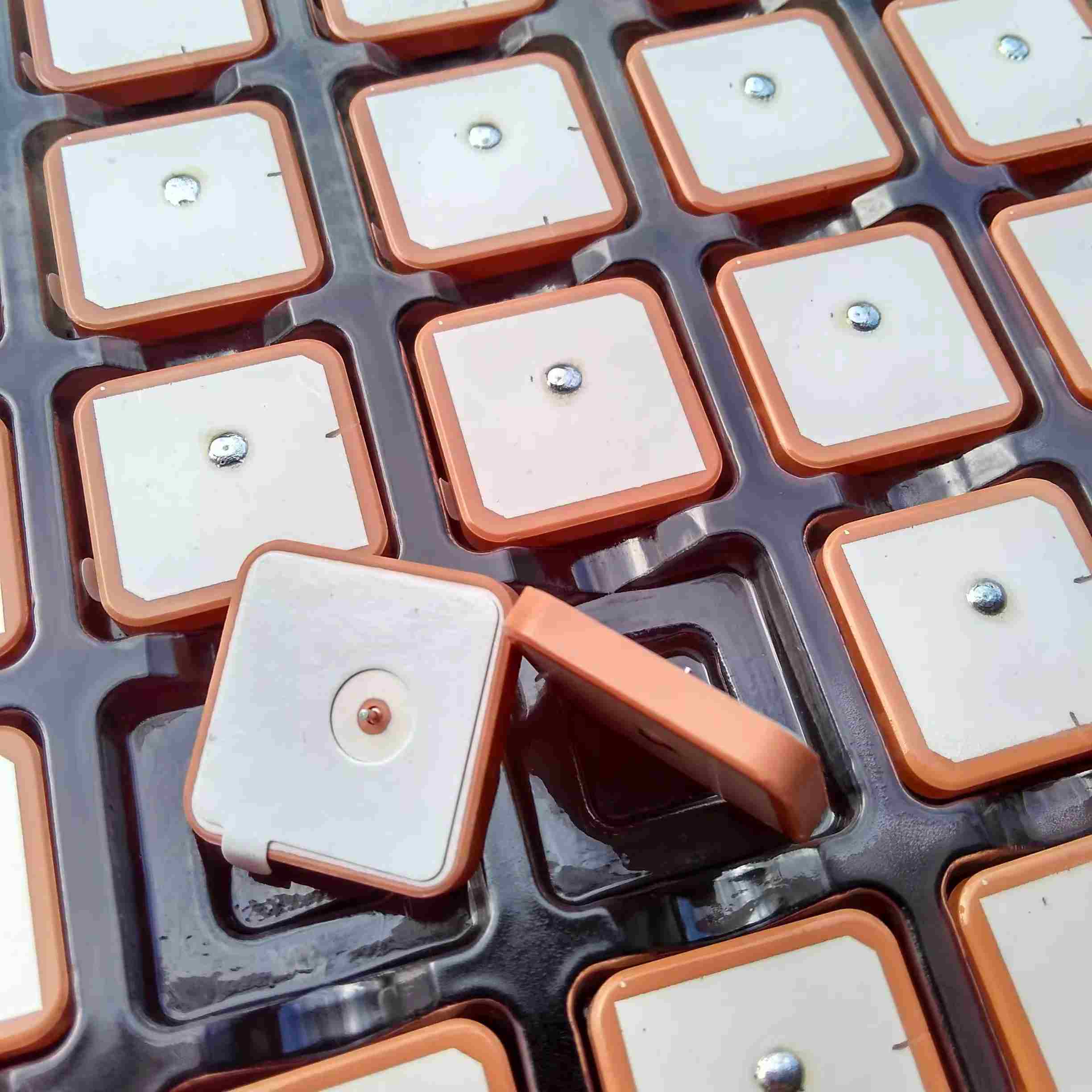
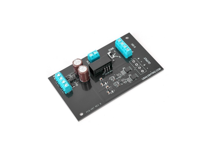
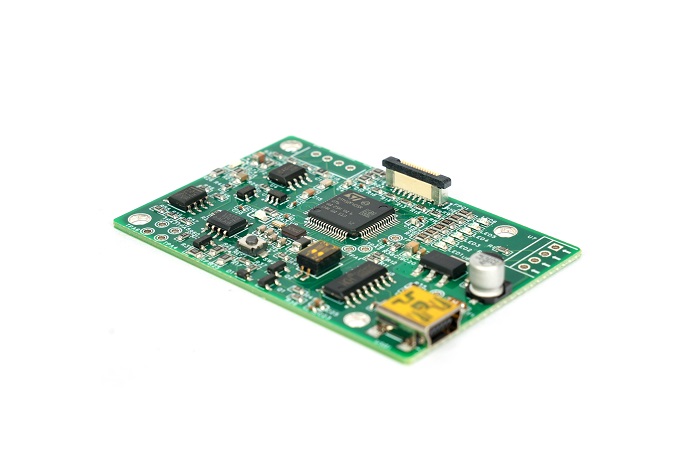
Common examples of active components include transistors, ICs (integrated circuits), diodes, LEDs, and relays.
These components are the “workhorses” of active and passive components in PCB design, enabling signal amplification and precise control in all electronic devices.
What Are Passive Components in Electronics? Definition & Examples
Passive components do not need external power to operate. They store or dissipate energy without amplifying signals, supporting the core function of active components.
Common examples of passive components include resistors, capacitors, inductors, and transformers.
They are essential for active and passive components for circuit design, handling filtering, timing, load matching, and energy storage.
What Is the Difference Between Active and Passive Components? Comparison Table
Knowing the key differences between these components ensures you select the right parts for your project. Below is a detailed comparison of active vs passive components.
| Feature | Active Components | Passive Components | Common Use Case |
|---|---|---|---|
| Power Requirement | Needs external power to operate | No external power required | All electronic circuits |
| Core Function | Amplify, switch, or control electrical signals | Store, dissipate, or transfer energy | Signal management and power regulation |
| Examples | Transistors, ICs, diodes, LEDs, relays | Resistors, capacitors, inductors, transformers | PCB design and circuit assembly |
| Energy Role | Supplies energy to the circuit | Uses or reserves energy from the circuit | Power systems and signal processing |
What Are the Advantages and Disadvantages of Active Components?
Understanding the advantages of active components and their limitations helps you make informed design decisions.
Advantages: High performance, signal amplification, precise control over circuit behavior, and ability to switch signals quickly.
Disadvantages: Higher cost compared to passive components, requires external power, and adds complexity to PCB design.
What Are the Advantages and Disadvantages of Passive Components?
The advantages of passive components make them indispensable for reliable, cost-effective circuits.
Advantages: Low cost, simple design, high reliability, no external power needed, and long service life.
Disadvantages: No signal amplification capability, limited function, and fixed electrical parameters that cannot be adjusted.
How to Choose Between Active and Passive Components?
Selecting between active and passive components depends on your circuit’s specific needs.
Use active components for amplification, switching, or signal control—ideal for circuits that need to boost or modify signals.
Use passive components for filtering, timing, load matching, or energy storage—critical for stabilizing circuits and managing power flow.
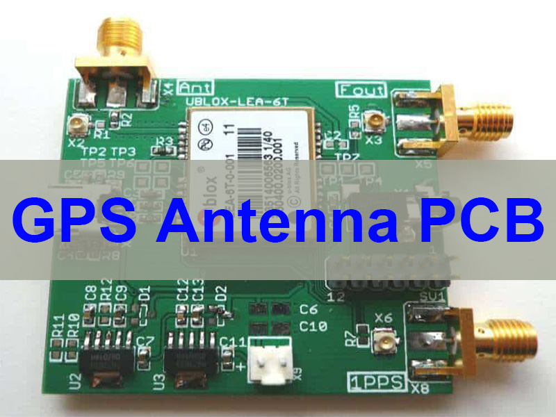
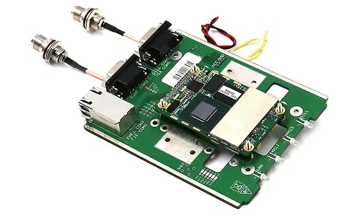
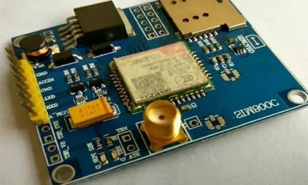
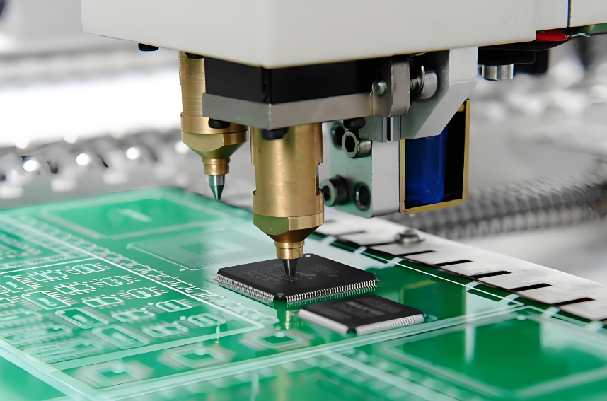
Active and Passive Components in PCB Design (Top 4 Industries)
Consumer Electronics
Smartphones, tablets, and wearables rely on active and passive components in consumer electronics.
ICs (active) and capacitors (passive) are used to ensure small size, low power consumption, and stable performance.
Automotive Electronics
EV controllers, infotainment systems, and safety modules use active and passive components in automotive electronics.
Transistors (active) and power resistors (passive) meet high reliability and temperature resistance standards for vehicle environments.
Industrial Control & Automation
PLCs (Programmable Logic Controllers) and factory automation systems use active and passive components in industrial electronics.
Relays (active) and inductors (passive) provide signal isolation and stability in harsh factory conditions.
Medical Electronics
Patient monitors, diagnostic devices, and medical implants use active and passive components in medical devices.
Op-amps (active) and precision passive components comply with strict safety and accuracy regulations for medical applications.
How to Identify Active and Passive Components?
Identifying active and passive components is simple with these key indicators.
Active components: Require a power pin or connection (e.g., ICs with VCC pins, transistors with base/emitter pins).
Passive components: No power connection needed (e.g., resistors with two leads, capacitors with two terminals).
Common Failures of Active & Passive Components & Fixes
Even high-quality active and passive components can fail—here’s how to troubleshoot and fix common issues.
Active components: Overheating or voltage damage → Use proper cooling solutions and voltage protection circuits.
Passive components: Parameter drift or short circuits → Select high-quality, rated parts from reliable suppliers.
How Do Active & Passive Components Affect PCB Quality & Supply Chain?
The quality of active and passive components directly impacts PCB performance and supply chain stability.
Quality: Choose certified components to ensure long-term reliability and compliance with industry standards.
Supply chain: Select widely available parts to avoid delays—EBest ensures a stable supply chain for electronic components.
Latest Trends for Active and Passive Components (2026)
The types of active and passive components with examples are evolving to meet industry demands in 2026.
Miniaturization: Smaller component packages for compact PCBs in consumer and medical devices.
High reliability: Automotive and medical grade components with enhanced durability and performance.
Sustainability: Low-power active components and eco-friendly passive components to reduce energy consumption.
FAQ: Frequently Asked Questions About Active and Passive Components
Is a transistor active or passive component?
A transistor is an active component. It requires external power to amplify or switch electrical signals, which is a key characteristic of active components.
Is a resistor active or passive component?
A resistor is a passive component. It dissipates energy as heat and does not require external power to operate, fitting the definition of passive components.
Is a capacitor active or passive?
A capacitor is a passive component. It stores electrical energy and releases it as needed, without requiring external power to function.
Do active components need power?
Yes, active components need external power. They cannot amplify or control signals without a power source, unlike passive components.
Do passive components need a power supply?
No, passive components do not need a power supply. They operate using the energy available in the circuit, such as storing or dissipating energy from active components.
Why are active and passive components important?
Active and passive components are important because they work together to create functional electronic circuits. Active components provide control and amplification, while passive components stabilize and support signal flow.
Active vs passive components which is better?
Neither is “better”—they serve different purposes. Active components are essential for signal control/amplification, while passive components are critical for stability and energy management. Both are required for most circuits.
Summary: Master Active and Passive Components for Better PCBs
active and passive components form the foundation of all electronic circuits. The function of active and passive components works in harmony to ensure circuits perform reliably, efficiently, and cost-effectively.
Correct selection of active and passive components improves PCB quality, reduces failures, and ensures your device meets industry standards.
EBest provides high quality PCB with active and passive components and reliable active and passive components for PCB manufacturing. We specialize in PCB manufacturing with active and passive components and custom PCB using active and passive components, with a stable supply chain and on-time delivery. If you need high-quality components and PCB solutions, place your order with us. Email us at sales@bestpcbs.com for inquiries and quotes.