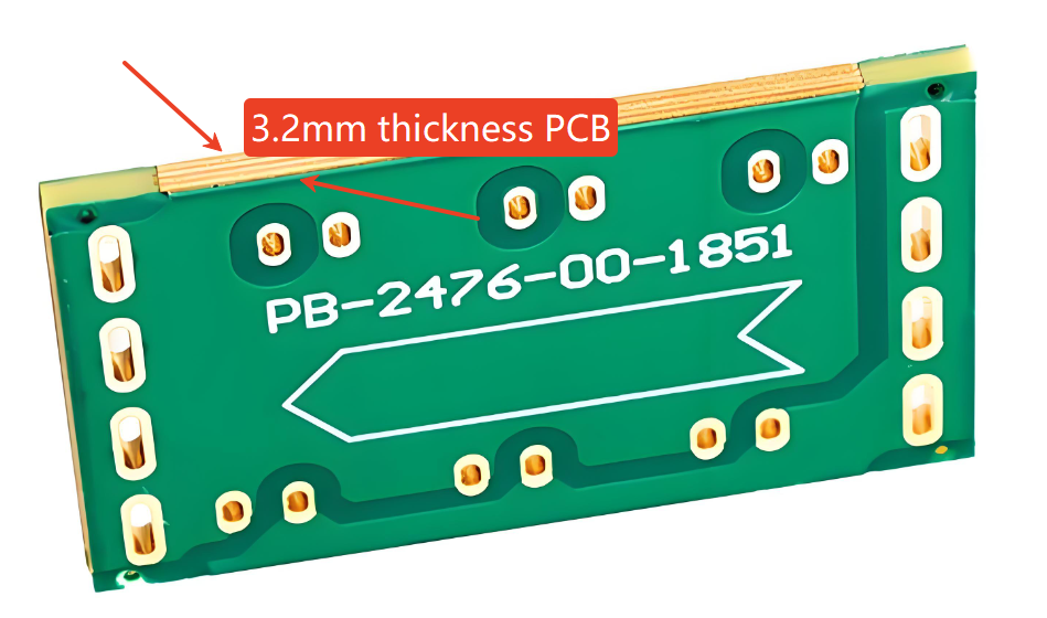
3.2mm to inches equals 0.12598 inches, commonly rounded to 0.126 inches.
lthough 3.2mm is often associated with 1/8 inch, it is slightly larger than 1/8″ (which equals 3.175mm). For general PCB fabrication, hardware selection, and sheet material, treating 3.2mm as ≈ 1/8 inch is acceptable. For tight-tolerance or mating components, always use the exact value: 0.12598 inches.
This conversion is frequently referenced in PCB thickness control, mechanical part matching, and cross-standard manufacturing, especially when metric-designed components are produced or assembled in imperial-based environments.
Engineering Method for Converting 3.2mm to Inches
All engineering-grade conversions rely on a fixed constant.
1 inch = 25.4 millimeters (exact, not approximate)
To convert millimeters to inches:
3.2 ÷ 25.4 = 0.12598 inches
In CAD systems, CAM outputs, and inspection reports, engineers usually keep four to five decimal places to prevent cumulative dimensional deviation. Rounding is applied only at the documentation or purchasing stage.
Why 3.2mm Is Widely Used in PCB and Mechanical Manufacturing?
3.2mm is considered a hybrid-standard thickness. It bridges metric design logic with imperial production habits.
In PCB manufacturing, 3.2mm is commonly selected for:
Power distribution boards
Backplanes and structural PCBs
Boards used as mounting or support elements
Industrial controller PCBs requiring stiffness
In mechanical manufacturing, 3.2mm sheet thickness is frequently used for:
Aluminum and steel brackets
Equipment enclosures
Protective covers and panels
This thickness offers good rigidity while remaining compatible with standard drilling, routing, and bending processes.
3.2mm to Inches Chart ((Fractional & Decimal)
The table below shows 3.2mm to inches alongside nearby metric sizes, including fractional inch equivalents commonly used in hardware, PCB thickness, and metal stock selection.
Millimeters (mm)
Fractional Inches
Decimal Inches
2.0 mm
5/64″
0.0787″
2.4 mm
3/32″
0.0937″
3.2 mm
≈ 1/8″
0.12598″ (≈ 0.126″)
3.5 mm
9/64″
0.1378″
4.0 mm
5/32″
0.1575″
4.8 mm
3/16″
0.1890″
6.4 mm
1/4″
0.2520″
Engineering note:
1/8 inch equals 3.175mm, not 3.2mm. The 0.025mm difference may matter in precision machining, PCB slot sizing, or press-fit applications.
Why 3.2mm Is Commonly Treated as 1/8 Inch?
In practice, 3.2mm is widely treated as a nominal 1/8-inch equivalent because:
The dimensional difference is very small
Standard drill bits and tooling align closely
PCB thickness tolerances usually exceed ±0.025mm
Hardware and sheet stock are often sold by nominal size
This is why datasheets, BOMs, and supplier listings frequently group 3.2mm and 1/8 inch together.
3.2mm to cm in Technical Documentation
3.2mm equals 0.32 cm.
This conversion is exact and does not involve rounding. It is often used in:
Engineering specifications
International standards
Educational and training materials
Centimeter notation is common in documentation intended for non-manufacturing audiences.
3.2mm to Feet in Industrial Context
3.2mm equals 0.0105 feet.
While feet are rarely used for small dimensions, this conversion may appear in:
Mixed-unit architectural layouts
Legacy documentation
Facility-level mechanical references
For fabrication work, inches or millimeters remain preferred.
Is 3.2mm the Same as 1/8 Inch in PCB and Mechanical Design?
No. 1/8 inch equals 3.175mm, not 3.2mm.
The difference is 0.025mm, which may seem negligible but can impact:
PCB edge connector fit
Slot and cutout tolerances
Press-fit components
Stack-up alignment in assemblies
In high-reliability PCB designs, this difference must be evaluated rather than assumed acceptable.
Practical PCB Applications of 3.2mm Thickness
In PCB fabrication, 3.2mm thickness is often chosen when mechanical strength is more important than weight reduction.
Typical PCB use cases include:
High-current power boards
Backplanes in industrial systems
PCBs acting as mechanical supports
Boards exposed to vibration or shock
Thicker boards reduce flexing, which helps protect solder joints and large components.
Manufacturing Implications of 3.2mm Thickness
From a production perspective, 3.2mm thickness affects multiple processes:
Drilling requires adjusted feed rates
Routing needs deeper cut passes
Plating thickness becomes more critical
Panel warpage control becomes more important
Manufacturers often adjust tooling and process parameters specifically for boards or parts at this thickness.
Metric vs Imperial Units in Global PCB Manufacturing
Most PCB designs originate in metric units. However, many:
Assembly fixtures
Test equipment
Mechanical interfaces
still follow imperial standards.
This creates frequent conversion scenarios where 3.2mm to inches must be clearly defined to avoid misinterpretation between design, fabrication, and assembly teams.
Common Engineering Errors When Converting 3.2mm to Inches
Errors often occur when:
Designers assume 3.2mm equals 1/8 inch
Finished thickness is confused with core thickness
Copper weight and surface finish are ignored
Units are converted without tolerance context
These mistakes can lead to fit issues, assembly delays, or rejected parts.
FAQs About 3.2mm to Inches
1. How many inches is 3.2mm?
3.2mm equals 0.12598 inches, which is commonly rounded to 0.126 inches for practical use. This value is widely accepted in engineering, PCB manufacturing, and hardware selection.
2. Is 3.2mm the same as 1/8 inch?
No. 3.2mm is slightly larger than 1/8 inch.
1/8 inch equals 3.175mm, while 3.2mm equals 0.12598 inches. The difference is small but can matter in precision applications.
3. Why is 3.2mm often called 1/8 inch?
3.2mm is often treated as 1/8 inch because the dimensional difference is minimal and usually falls within standard manufacturing tolerances. Many suppliers group these sizes together for convenience.
4. Is 3.2mm a standard PCB thickness?
Yes. 3.2mm is a common PCB thickness, especially for power boards, backplanes, and mechanically reinforced PCBs. It provides higher rigidity compared to thinner boards.
5. Can 3.2mm replace 1/8 inch material?
In most cases, yes.
For sheet metal, PCB panels, and brackets, 3.2mm can replace 1/8 inch. Always verify tolerance requirements for mating or press-fit parts.
6. What is the formula to convert 3.2mm to inches?
The formula is:
Inches = millimeters ÷ 25.4
3.2 ÷ 25.4 = 0.12598 inches
7. Does PCB copper thickness affect the final 3.2mm board thickness?
Yes. The finished PCB thickness includes laminate, copper layers, and surface finish. Copper weight and plating can slightly increase the final thickness beyond the nominal 3.2mm.
MCX Connector PCB is a critical high-frequency interconnect solution that mounts Miniature Coaxial (MCX) connectors directly onto printed circuit boards, enabling reliable RF signal transmission in compact electronic assemblies. This comprehensive guide explores the design, selection, application, and manufacturing of MCX connector PCBs, with a focus on the complete turnkey process from initial design to final assembly.
For engineers sourcing MCX connector PCBs, the path from concept to a fully functional, mass-produced RF board is fraught with challenges. What are the most common pain points developers face when integrating these specialized components?
Signal Degradation and Mismatch: Improper impedance control or layout around the MCX PCB connector footprint causes significant RF signal loss, return loss, and degraded system performance.
Mechanical Failure in the Field: Choosing a connector with inadequate locking mechanism or PCB retention can lead to intermittent connections or the MCX connector detaching from the PCB under vibration.
Prototyping Bottlenecks: Difficulty in obtaining small-batch, reliable prototypes for testing from suppliers who only focus on high-volume orders, stalling the design verification phase.
Inconsistent Quality in Volume: Receiving production batches with poor soldering, misaligned connectors, or inconsistent plating that fails during assembly or compliance testing.
Hidden Costs and Timeline Delays: Unexpected expenses and delays arise from dealing with multiple vendors for design, PCB fabrication, connector sourcing, and assembly, coupled with poor communication.
Here is how a full-turnkey service model directly addresses these critical issues.
Expert RF Design Review: A specialized manufacturer provides upfront Design for Manufacturability (DFM) and Design for Excellence (DFX) analysis specifically for RF layouts, ensuring optimal impedance matching and placement to eliminate signal integrity issues from the start.
Validated Component Sourcing: Leveraging direct relationships with trusted connector manufacturers (like those producing China MCX connector PCB components) to supply genuine, mechanically robust connectors with verified specifications for reliable mating and board retention.
Rapid Prototyping Services: Offering fast-turn, low-volume prototype builds that use the same processes as mass production, allowing for real-world performance validation without delaying the project timeline.
Integrated High-Precision Manufacturing: Controlling the entire production line—from PCB fabrication with tight impedance tolerance to automated, optical-inspected assembly—ensures consistent, high-quality output in every batch, whether for prototypes or volume runs.
Unified Project Management: A single point of contact and responsibility for the entire full turnkey process—from initial design files to final assembled and tested boards—eliminates vendor coordination hassles, provides cost transparency, and guarantees on-time delivery.
At BEST Technology, we specialize in providing exactly this seamless, end-to-end service. As a professional MCX connector PCB factory, we combine deep RF expertise with advanced manufacturing capabilities to deliver reliable, high-performance boards. From selecting the right PCB MCX male connector to ensuring flawless assembly, we manage every detail, allowing you to focus on your core product development. Pls feel free to contact our team at sales@bestpcbs.com to transform your RF board requirements into a perfected product.
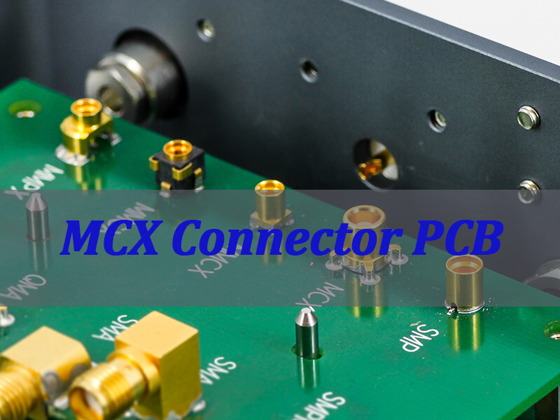
What Is an MCX Connector PCB?
An MCX Connector PCB refers to a printed circuit board that incorporates Miniature Coaxial (MCX) connectors as integrated board-mount interfaces. These connectors are known for their compact size, snap-on coupling mechanism, and excellent performance through several GHz, making them ideal for space-constrained RF applications.
Core Components: The system consists of the PCB itself (with controlled-impedance traces), the connector’s solderable footprint, and the MCX PCB connector (male or female) which is soldered onto the board.
Key Interface: It serves as the critical transition point between the controlled environment of the PCB trace and the external coaxial cable, minimizing signal reflection and loss.
Common Formats: Boards can feature various layouts, including edge-mounted connectors, through-hole designs, or MCX jack panel PCB connector arrays for chassis interfaces.
In essence, an MCX Connector PCB is a fundamental building block in modern RF systems, enabling efficient and reliable high-frequency signal ingress and egress in a miniaturized format. Choosing a reliable pcb mcx jack connector factory is crucial for ensuring the performance of this critical link.
Where Is MCX Connector PCB Commonly Used in RF Systems?
MCX connector PCBs are ubiquitous in applications where a blend of small form factor, reliable RF performance, and moderate frequency requirements converge. Their usage spans commercial, consumer, and industrial sectors.
Application Sector
Specific Use Cases
Why MCX is Preferred
Telecommunications
Cellular repeaters, base station subsystems, GSM MCX PCB connector modules, antenna feeder links.
Compact size, good performance at cellular bands (e.g., 900 MHz, 1800 MHz).
IoT & Wireless Devices
Wireless sensors, RFID readers, LPWAN gateways, short-range communication modules (Bluetooth, Zigbee).
Saves valuable board space in compact devices.
Test & Measurement
Portable analyzers, signal generator modules, internal interconnects in lab equipment.
Allows for dense connector arrangements on panels.
Broadcast & AV
Digital video broadcast (DVB) equipment, satellite receiver LNBs, in-car entertainment systems.
Reliable performance for video/audio signal transmission.
Aerospace & Defense
Avionics comms, UAV telemetry, GPS modules, and other space-constrained onboard systems.
Lightweight and secure snap-on mating withstands mild vibration.
From enabling the GSM backhaul in remote locations to connecting antennas on a compact IoT sensor, the MCX connector PCB is a versatile workhorse. The trend towards miniaturization continues to drive its adoption, making a partner like a proficient China PCB MCX male connector supplier essential for developers worldwide.
Key Structural Differences Between MCX PCB Connectors and Other RF PCB Mount Connectors
Selecting the right RF connector involves understanding mechanical and electrical trade-offs. MCX, SMA, and SMP are common choices, each with distinct structural advantages.
1. Coupling Mechanism:
MCX: Uses a snap-on, quick-connect/disconnect interface. It mates with a simple push and releases with a gentle pull, offering speed but a relatively lower mating security compared to threaded types.
SMA: Features a robust threaded coupling mechanism. It provides very high mechanical stability and superior shielding but requires more time and space for wrench tightening.
SMP (SubMiniature Push-on): Offers a slide-on/push-off action with a distinct detent. It provides a good compromise between MCX’s speed and SMA’s security, often used for blind-mate applications.
2. Size and Weight:
MCX: Has the smallest outer diameter (~3.5mm) and is very lightweight, enabling the highest port density on a panel PCB connector.
SMA: Significantly larger and heavier (~5mm+ diameter), reducing the number of connectors that can be placed in a given area.
SMP: Slightly larger than MCX but smaller than SMA, offering a dense yet more secure alternative.
3. Frequency Performance:
MCX: Typically rated for reliable operation up to 6 GHz, suitable for many commercial wireless applications.
SMA: A true workhorse, often specified for performance up to 18 GHz or even 26.5 GHz in precision versions.
SMP: Can perform into the millimeter-wave range, with many variants rated for 40 GHz and beyond.
4. Mechanical Durability:
MCX: Rated for around 500 mating cycles. Its plastic snap-ring is the wear point, making it suitable for applications not requiring frequent connection changes.
SMA: Can withstand 500+ mating cycles (with metal-on-metal threading), ideal for test equipment and field-deployed gear.
SMP: Mating cycle life varies by design but generally falls between MCX and SMA.
In summary, the MCX PCB connector is the choice for ultimate miniaturization and quick connection where extreme mechanical robustness or ultra-high frequency is not the primary driver. Its structure defines its niche in the RF interconnect ecosystem.
How to Select the Right MCX PCB Connector for Signal Integrity and Mechanical Stability?
Choosing the optimal MCX connector is a balancing act between electrical performance and physical reliability. Key factors must be evaluated against your specific application requirements.
1. Impedance Matching: The connector must be 50Ω (standard for RF) to match your controlled-impedance PCB trace. Any mismatch creates signal reflections (high VSWR). Verify the connector’s datasheet impedance specification.
2. Frequency Range & VSWR: Check the connector’s rated maximum frequency and its Voltage Standing Wave Ratio (VSWR) performance across your band of operation. A lower, flatter VSWR (e.g., <1.3:1) indicates better signal integrity.
3. Interface Gender and Configuration: Decide between a PCB MCX male connector (pin) or a female (socket) for board-mount. Consider if you need a straight, right-angle, or edge-mount type based on your board layout and cable routing.
4. Termination and Retention: Evaluate the PCB tail style (surface-mount/SMT or through-hole) and the board retention features. SMT saves space, but through-hole provides stronger mechanical bonding. Look for connectors with solder tabs or mounting ears for enhanced stability, especially for the PCB mount female MCX switch connector types that may see actuation force.
5. Material and Plating: The center contact is typically beryllium copper for spring properties, plated with gold over nickel for low resistance and corrosion resistance. The outer body/collet should be brass or similar, with a corrosion-resistant finish. Inferior plating increases insertion loss and degrades over time.
6. Mating and Unmating Force: Ensure the connector’s specified mating force aligns with your assembly process and end-use. Too high a force can damage the board; too low can lead to unreliable connections.
By systematically analyzing these factors against your operational environment (temperature, vibration, mating cycles) and signal requirements, you can select an MCX PCB connector that ensures both a clean signal path and long-term reliability on the board.
Design Considerations When Integrating GSM MCX PCB Connector Into RF and IoT Boards
A GSM MCX PCB Connector is a specific type of MCX connector PCB interface designed and optimized for use in GSM (Global System for Mobile Communications) frequency bands, primarily 850/900 MHz and 1800/1900 MHz. It is selected for its compact size and adequate performance within these cellular ranges, commonly found in modules, repeaters, and IoT devices with cellular connectivity.
Integrating a GSM MCX PCB connector successfully requires attention to both RF principles and practical layout constraints to ensure the module performs as intended in the final product.
1. Impedance Continuity is Paramount: The 50-ohm microstrip or coplanar waveguide trace leading to the connector must be designed with precise width and spacing, considering the PCB stack-up. The transition from the trace to the connector pad must be as smooth as possible to minimize discontinuities. Use simulation tools if available.
2. Grounding and Via Fencing: Provide an excellent, low-inductance RF ground for the connector. This involves:
Placing a dense array of grounding vias (a “via fence”) immediately around the connector’s ground pads.
Ensuring ground pours on multiple layers are stitched together with vias to form a solid ground cage, preventing parasitic modes.
3. Keep-Out and Component Placement: Maintain a clear keep-out area around the connector footprint, especially in the direction of the mating interface. Do not place tall components nearby that could obstruct cable attachment. Keep sensitive analog or high-speed digital traces away from the RF path to avoid coupling.
4. Mechanical Reinforcement: For applications subject to vibration or where the cable may be stressed, consider adding mechanical support. This can include:
Using through-hole connector variants for stronger bond.
Adding epoxy strain relief spots on the connector body after soldering (often done in assembly).
Designing a board cut-out or chassis support to take lateral force off the solder joints.
5. DFM/DFA for Assembly: Design the footprint according to the connector manufacturer’s recommended land pattern. Ensure solder paste stencil apertures are correctly sized to prevent tombstoning (for SMT types) or solder voids. Clear silkscreen markings for orientation aid assembly technicians.
In practice, a well-integrated GSM MCX PCB connector should appear electrically “invisible” at its operating frequency, providing a seamless, low-loss transition between the board and the antenna system. Neglecting these considerations can lead to reduced range, dropped connections, and failed compliance tests.
Manufacturing Capabilities of a Reliable MCX Connector PCB Factory for Volume Production
A factory capable of delivering high-volume, reliable MCX connector PCBs must possess a tightly integrated set of capabilities that span materials, precision fabrication, and automated assembly. This is what separates a true turnkey partner from a simple board fab house.
Advanced PCB Fabrication: Expertise in producing boards with tightly controlled dielectric constants (Dk) and loss tangents, and impedance control with tolerances of ±5% or better. This includes mastery of materials like FR-4, Rogers, or hybrid stacks.
Automated, High-Precision Assembly: Utilizing chip shooter and fine-pitch placement machines for accurate SMT component placement, coupled with advanced solder paste inspection (SPI) and reflow profiling to ensure perfect soldering of the tiny MCX PCB connector leads.
Stringent Quality Control Regime: Implementing a multi-stage inspection protocol including Automated Optical Inspection (AOI) for solder joint quality, X-ray inspection for hidden voids (especially on BGA or under connectors), and 100% electrical testing of the RF path for continuity and shorts.
Supply Chain Mastery: Established, vetted relationships with top-tier connector manufacturers to ensure a steady supply of authentic, high-performance MCX PCB connectors, avoiding counterfeit or substandard components that plague the market.
Scalable Process Engineering: The ability to seamlessly scale from a few prototype boards to thousands of production units while maintaining consistent quality. This involves process optimization, fixture design for panelization, and efficient throughput.
A reliable MCX connector PCB factory like BEST Technology combines these capabilities under one roof. This vertical integration and control over the entire process—from sourcing the right China MCX connector to final RF testing—is what guarantees a manufacturable design and a flawless, on-schedule production run for our clients.
What Determines the Cost Structure in an MCX Connector PCB Pricelist?
Understanding the MCX connector PCB pricelist requires breaking down the cost drivers at each stage of the turnkey process. Transparency here helps in budgeting and value engineering.
Cost Driver Category
Specific Factors
Impact on Final Cost
PCB Fabrication
Board material (FR-4 vs. RF laminate), layer count, board size/panel utilization, impedance control tolerance, surface finish (ENIG), and special requirements (like blind vias).
This forms the base substrate cost. High-frequency materials and tight tolerances increase cost.
Component Cost
The unit price of the MCX PCB connectors themselves, which varies by brand, plating quality, and configuration (e.g., right-angle vs. straight). Switches or other special components also add cost.
A significant portion of the BOM cost, especially for high-quality, brand-name connectors.
Assembly Complexity
Number of components, mix of technology (SMT vs. thru-hole), density, and need for special processes (e.g., underfill, selective soldering for a PCB mount female MCX switch connector).
Higher complexity requires more sophisticated equipment and time, increasing labor and machine costs.
Testing & Qualification
Level of testing required: basic continuity, full functional test, or RF parameter verification (VSWR, insertion loss). Fixture development costs for automated testing.
More comprehensive testing adds upfront engineering and per-unit time costs but reduces field failure risk.
Order Volume & Logistics
Economies of scale: unit cost drops significantly with higher volumes. Packaging requirements and shipping destination also factor in.
Prototypes are inherently higher cost per unit. Large volumes spread fixed costs (setup, tooling) over more units.
When reviewing a pricelist, it’s crucial to look beyond the simple per-board quote. The value lies in a supplier’s ability to optimize these factors—through smart material selection, efficient panel design, and bulk purchasing—to deliver the required performance at the best total cost of ownership. Requesting a detailed breakdown from your MCX connector PCB factory is always a best practice.
Application Scenarios for PCB Mount Female MCX Switch Connector in Compact RF Devices
The PCB mount female MCX switch connector is a specialized variant that integrates a switching function—typically between an internal antenna path and an external port—directly onto the board. This component is invaluable for adding flexibility and testability to space-constrained designs.
1. Internal/External Antenna Selection: The most common use. The switch allows the RF transceiver to connect to either a small, integrated PCB antenna or an external, high-gain antenna via the MCX port. This is crucial for devices that may be used in varying signal strength environments.
2. Production Line Testing and Calibration: The switch connector provides a dedicated, easily accessible test point. During manufacturing, test equipment can be connected to calibrate output power, frequency, and modulation accuracy without interfering with the operational antenna, speeding up the testing process.
3. Field Diagnostics and Maintenance: For deployed equipment, a technician can connect a portable analyzer to the external port to diagnose signal issues without opening the device casing, enabling quick troubleshooting and minimal downtime.
4. Signal Path Bypass or Loopback: In some designs, the switch can be used to create a controlled loopback path from the transmitter to the receiver for self-test or diagnostic routines, improving system reliability.
5. Multi-mode Device Configuration: In devices that support multiple communication standards (e.g., Cellular + GPS), a switch can be used to route signals from different internal modules to a common external antenna connector, simplifying the mechanical design.
By integrating this functionality, the PCB mount female MCX switch connector saves significant board space compared to using a separate RF switch IC and connector. It simplifies the RF front-end layout, reduces component count, and enhances the device’s field utility, making it a strategic component in sophisticated compact devices. Partnering with an expert PCB MCX male connector factory that understands these applications ensures you get a component that meets both electrical and mechanical lifecycle requirements.
Why Engineers Purchase China MCX Connector PCB from EBest Circuit (Best Technology)?
Engineers and procurement specialists globally turn to BEST Technology for their China MCX Connector PCB needs because we solve the core dilemma: achieving high-performance, reliable RF boards at a scalable cost without compromising on service or technical expertise. We are not just a supplier; we are a full-turnkey engineering and manufacturing partner.
End-to-End Ownership: We manage the entire process—from design review and PCB MCX connector sourcing to fabrication, assembly, and testing. This single-point accountability eliminates finger-pointing between vendors and ensures seamless project execution.
Deep RF & Manufacturing Expertise: Our engineering team possesses specialized knowledge in RF layout and DFM. We proactively identify and resolve potential signal integrity or manufacturability issues before they become costly prototypes or production delays.
Uncompromising Quality with Cost Efficiency: By operating our own advanced manufacturing facilities and leveraging our position in the robust China PCB supply chain, we control quality at every step while optimizing costs. This allows us to offer a compelling MCX connector PCB pricelist without cutting corners on materials or processes.
Scalability from Prototype to Volume: We support you at every stage. We deliver fast, functional prototypes for validation and seamlessly transition to high-volume manufacturing with consistent quality, ensuring your time-to-market is accelerated.
Proactive Communication and Support: We assign a dedicated project manager to every order, providing clear, timely updates and acting as your technical liaison. We believe transparent partnership is key to success.
Choosing BEST Technology means investing in a hassle-free pathway from concept to a high-quality, assembled board. We provide the certainty, performance, and partnership that complex RF projects demand.
Overall, MCX Connector PCBs are essential, high-performance interconnects that enable reliable RF signal transitions in increasingly miniaturized and complex electronic devices. This guide has comprehensively covered their definition, application, selection, design, and manufacturing, highlighting the critical importance of a integrated approach from design to assembly.
For projects where performance, reliability, and timeline cannot be left to chance, partnering with an expert full-turnkey provider is the most strategic decision. BEST Technology embodies this partnership, combining deep RF engineering insight with vertically controlled manufacturing to deliver superior MCX Connector PCBs. Let us manage the complexities so you can focus on innovation. A warm welcome to contact our technical sales team at sales@bestpcbs.com for a consultation and quote.
Looking for PCB manufacturer in Sri Lanka? This blog breaks down top local manufacturers, practical selection tips, industry challenges, and how EBest Circuit (Best Technology) addresses them helping you make informed sourcing decisions.
When sourcing PCBs, finding a reliable PCB Manufacturer in Sri Lanka that balances quality, speed, and cost is crucial for electronics businesses. As a leading global PCB Manufacturer in Sir Lanka, EBest Circuit (Best Technology) Co.,Ltd stands out among local players by integrating global standards with localized service solving the core pain points of both Sri Lankan startups and international brands.
Top PCB Manufacturer in Sri Lanka List
Company Name
Core Business
Manufacturing Capability
Lead Time
EBest Circuit (Best Technology) Co.,Ltd
Rigid/Flex PCB, PCB Assembly, Custom PCB for Medical/Auto
Seek manufacturers with globally recognized certifications such as ISO 9001, UL certification, or RoHS compliance. For example, Aptinex (a leading Sri Lankan PCB manufacturer) adheres to international quality standards and offers services from PCB prototyping to mass production. Certifications validate technical expertise and regulatory compliance, ensuring reliability for global markets.
2. Assess Technical Expertise & Production Capabilities
Evaluate the manufacturer’s ability to handle complex designs (e.g., multilayer PCBs, HDI, or flexible circuits). Aptinex demonstrates advanced capabilities through SMT/THT component assembly and firmware development, indicating robust technical infrastructure. Prioritize manufacturers with in-house prototyping, drilling, and assembly lines to ensure vertical integration and quality control.
3. Review Quality Control Processes
Investigate automated defect detection systems and real-time monitoring. While specific PCB examples are limited, Sri Lanka’s apparel industry uses systems like SeamSense (leveraging machine learning for defect detection). Look for similar quality assurance protocols, such as motion-adaptive frame extraction or model-based augmentation, to minimize defects and ensure consistency.
4. Evaluate Industry Reputation & Customer Testimonials
Prioritize manufacturers with verifiable client portfolios or case studies. DHL’s emphasis on customer loyalty in Sri Lanka highlights the importance of trust in B2B relationships. Seek references from global clients or partners to validate reliability. Avoid manufacturers lacking transparent client feedback or case studies.
5. Analyze Lead Times & Scalability
Inquire about production lead times and scalability to meet demand fluctuations. Factors like logistics efficiency and supply chain resilience impact delivery times. For example, Alibaba’s insights on Sri Lankan manufacturing stress the need for scalable production and reliable logistics to avoid delays, especially for export-oriented businesses.
6. Ensure Cost Transparency & Fair Pricing
Compare pricing structures to avoid hidden fees. Transparent pricing builds trust and long-term partnerships. Request detailed quotes outlining material costs, labor, and any additional charges. Manufacturers like Aptinex often provide clear cost breakdowns for prototyping and mass production.
7. Assess Communication & Technical Support
Effective communication is critical. Prioritize manufacturers with responsive support teams and clear channels (e.g., email, phone, or chat). Look for technical expertise in PCB design, material selection, and troubleshooting to address challenges promptly.
8. Conduct Site Visits or Audits (If Feasible)
If possible, visit the facility to assess equipment, cleanroom standards, and operational workflows. Direct observation confirms adherence to safety, quality, and environmental standards, enhancing trust in the manufacturer’s capabilities.
9. Review Contract Terms & IP Protection
Ensure contracts include clear terms on intellectual property (IP) ownership, confidentiality, and dispute resolution. Protect your designs and innovations through legally binding agreements. Avoid vague clauses that could lead to disputes over ownership or liability.
10. Leverage Industry Networks & Referrals
Seek recommendations from trusted industry peers, trade associations, or export agencies. Sri Lanka’s Colombo Development Dialogues (a knowledge-sharing initiative) highlights collaborative opportunities. Networking within regional manufacturing hubs can uncover reliable, vetted manufacturers.
Why do my PCB orders always arrive 2-3 weeks late, even with a confirmed timeline?
How to avoid getting PCBs with hidden defects that only show up during assembly?
Why can’t local manufacturers handle my 12-layer PCB design for industrial equipment?
Why do quotes jump by 30% after placing an order, with “unexpected material costs” as the excuse?
How to find a supplier that responds to technical issues outside working hours?
Our Solutions to These Challenges
On-Time Delivery Rate ≥98%: 3-month raw material stock + local supplier network cuts lead times by 50%. A telecom client’s 10,000-unit order was delivered 5 days early, helping them hit 5G rollout targets.
Defect Rate ≤0.2%: Triple inspection (AOI+X-ray+IPC-certified manual check) and 30-day quality guarantee. A medical device maker reduced rework costs by $12,000/year after switching to us.
100% Transparent Pricing: Detailed quotes with material breakdowns; no hidden fees. A startup avoided a $2,000 cost hike when we clarified copper price terms upfront.
24/7 Technical Support: Dedicated account managers respond within 1 hour. A night-shift assembly team solved a soldering issue via our live chat, minimizing downtime.
Why Sri Lanka Clients Choose EBest Circuit (Best Technology) for PCB Manufacturer?
Reasons Why Sri Lanka Clients Choose EBest Circuit (Best Technology) for Global PCB Manufacturer:
Competitive Pricing & Localized Supply Chain: Leverage 8+ local material partners to reduce import costs by 10–15% compared to average Sri Lankan PCB manufacturers. Example: A telecom client saved $35,000 annually on PCB expenses after switching.
Cost-Optimized Design Solutions: Analyze schematics to replace high-cost components (e.g., 10-layer → 8-layer optimization) without compromising performance. A consumer electronics brand reduced per-unit costs by $2.30 for a 50,000-unit order.
24-Hour Rapid Prototyping: Utilize automated SMT lines for 1–10 layer prototypes delivered within 24 hours—3x faster than 95% of local competitors. A startup met investor deadlines 2 days early.
99.2% On-Time Delivery Rate: Maintain 3-month raw material inventory and real-time logistics tracking to ensure 99.2% on-time delivery. A medical client avoided $8,000 in late penalties last year.
100% Full Inspection for Bulk Orders: Apply AOI, X-ray, and functional testing to every bulk order (0.2% defect rate, verified by client cases). An industrial control client reduced rework from 7% to 0.2%.
Global Compliance Certifications: Hold ISO 9001, IATF 16949 (automotive), ISO 13485 (medical), and RoHS certifications. A client exported 50,000+ PCBs to the EU without compliance delays.
19-Year Expertise & Error Database: Leverage a 10,000+ entry error database from 19 years of production to prevent common design flaws, cutting trial-and-error costs by 50% on average.
Free DFM Analysis by IPC-Certified Engineers: Identify and resolve issues like impedance mismatches early. A RF client avoided $12,000 in rework for a 20-layer PCB design.
One-Stop Service for Streamlined Projects: Cover PCB design, production, assembly, and testing under one roof, saving clients 20+ hours per project. An IoT client reduced project management time by 23 hours per order.
Localized Support for Real-Time Collaboration: Access Colombo-based teams via in-person meetings and a 24/7 local hotline. A university lab resolved a technical issue in 45 minutes (vs. 3 days with an overseas supplier).
Project Background: In 2025, a Sri Lankan electronics manufacturer sought to upgrade its local electronics manufacturing capabilities to meet international customer demands for high-precision, short-lead-time, and cost-effective double-sided/multilayer PCBs. As a technical partner, we provided end-to-end support from process optimization to mass production.
Project Requirements
Technical Specifications: Support 0.2mm line width/spacing, 2-12 layer board design, impedance control accuracy ±8%, compliant with IPC-A-600G Class 2 standards.
Delivery Timeline: Sample delivery within 3-5 working days, bulk orders within 7-10 working days.
Cost Control: Achieve 15% reduction in unit area cost compared to Sri Lanka’s market average while maintaining a yield rate of ≥95%.
Sustainability: Adopt lead-free soldering processes, comply with RoHS standards, and reduce production waste by 20%.
Solutions Implemented:
Process Optimization: Introduced Laser Direct Imaging (LDI) technology to replace traditional exposure methods, enhancing line width consistency. Adopted Vertical Continuous Plating (VCP) to improve via reliability.
Process Reengineering: Implemented a Manufacturing Execution System (MES) for full production traceability, paired with AI-powered visual inspection systems for automated defect detection.
Supply Chain Integration: Established a localized warehouse in Colombo to stock common substrates (e.g., FR-4, high-frequency materials) and secured long-term agreements with local etching solution suppliers to reduce costs.
Talent Development: Trained 15 certified engineers through on-the-job training (OJT) programs to master critical operational processes.
Project Outcomes
Efficiency Gains: Sample lead time reduced by 40%, bulk order on-time delivery rate reached 98%.
Cost Optimization: Unit cost decreased by 18%, exceeding project targets. Annual production capacity expanded from 50,000m² to 120,000m².
Quality Improvements: Yield stabilized at 96.5%, customer complaint rate dropped by 60%, and NADCAP certification achieved.
Market Expansion: Successfully entered the European electric vehicle supply chain, securing orders from Siemens (Germany) and ABB (Switzerland).
Sustainable Benefits: Production waste reduced by 22%, unit energy consumption lowered by 10%, and awarded Sri Lanka’s Green Manufacturing Certification.
How to Get a Quote for Your PCB Project?
To receive an accurate and efficient PCB quote, submit the following materials in a structured, clear format. Each item ensures precise cost estimation and production feasibility:
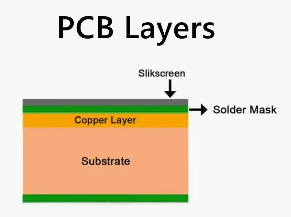
PCB layers are the physical and electrical building blocks of a printed circuit board. It is a layered structure made by stacking copper and insulating materials together. Each layer serves a clear purpose, such as carrying signals, distributing power, or providing a stable ground reference. The way these layers are arranged directly affects how the board performs.
What are layers on a PCB?
A PCB is not just a flat sheet. It is a carefully stacked structure. Each layer has a clear job. Together, these layers allow electricity to flow in a controlled way.
At the most basic level, a PCB layer can be copper, insulation, or surface coating. Copper layers carry signals and power. Insulation layers keep signals apart. Surface layers protect the board and make assembly possible.
PCB board layers define how complex a board can be. A simple product may need only two layers. A high-speed device may need many more. Each added layer increases routing space. It also improves signal control.
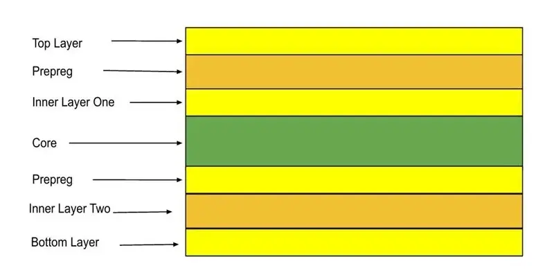
The layers of a PCB are planned during design. Engineers decide how many layers are needed. They also decide what each layer will do. This plan is called a PCB layer stackup.
Understanding PCB layers meaning helps avoid design mistakes. It also helps control cost. Too many layers waste money. Too few layers cause noise and routing problems.
At EBest Circuit (Best Technology), PCB layers design is part of our turnkey EMS service. From layout to final assembly, layer planning is handled early. This reduces risk and shortens lead time.
How are PCB layers produced?
PCB layers are produced through a precise and repeatable process. Each step matters. Small errors can affect the entire board.
The process starts with copper-clad laminate. This material has copper bonded to fiberglass. The fiberglass is usually FR-4. It offers strength and heat resistance.
For inner layers, copper is first etched. A photo image defines the circuit pattern. Chemicals remove unwanted copper. What remains forms the traces.
After etching, inner layers are inspected. Alignment is checked. Shorts and opens are detected early.
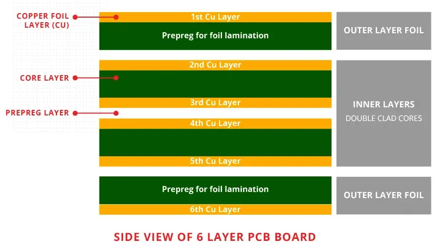
Next comes lamination. Multiple etched layers are stacked together. Prepreg sheets are placed between them. Heat and pressure bond everything into one board.
Once laminated, holes are drilled. These holes connect different PCB copper layers. Copper plating coats the hole walls. This creates electrical paths between layers.
Outer layers are then formed. The same imaging and etching steps apply. Finally, solder mask and surface finish are added.
Throughout this process, PCB layers stack up accuracy is critical. Even slight shifts can cause failures. At EBest Circuit (Best Technology), automated inspection ensures layer alignment stays within tight limits. Because we control both PCB fabrication and assembly, feedback is fast. That is a key benefit of turnkey EMS services.
What does a 2 layer PCB mean?
A 2 layer PCB is the most common board type. It has copper on the top and bottom. Between them is an insulating core.
In a PCB 2 layers design, components usually sit on the top. Traces run on both sides. Vias connect the two copper layers. This structure is easy to understand. It is also cost-effective. That is why many consumer products use it.
However, routing space is limited. Power and signal traces share the same layers. This can cause noise in sensitive circuits. Still, for low-speed designs, a two-layer board works well. Simple power supplies often use this type. Basic controllers also fit well.
At EBest Circuit (Best Technology), we manufacture high-quality two-layer boards at scale. Even simple boards benefit from good material and process control.
What does a 4 layer PCB mean?
A 4 layer PCB adds two inner copper layers. This design offers more control and flexibility. It is common in modern electronics.
A typical 4 layers PCB stackup includes:
Top signal layer
Inner ground layer
Inner power layer
Bottom signal layer
This structure separates signals from power. It also reduces noise. Signals return through a solid ground plane. A PCB 4 layers design allows shorter traces. It improves impedance control. This matters for fast digital signals.
In a 4 layers PCB, routing becomes cleaner. Components have more placement freedom. EMI issues are easier to manage. Cost is higher than two layers. Performance is much better.
At EBest Circuit (Best Technology), four-layer boards are a common request. They fit well in industrial control and communication products.
Do PCB layers matter?
Yes, PCB layers matter a lot. They affect performance, reliability, and cost. More layers provide better signal integrity. They allow clean power distribution. They also reduce electromagnetic interference.
Layer count affects thermal behavior. Inner planes help spread heat. This protects sensitive components.
PCB layers also affect manufacturing yield. Complex stackups need tighter control. That is why experience matters.
Choosing the wrong number of layers can cause redesigns. Redesigns cost time and money. At EBest Circuit (Best Technology), engineers review layer decisions early. This avoids later issues. It is part of our turnkey EMS approach.
How to identify PCB layers?
Identifying PCB layers depends on tools and experience. There are several common methods.
The simplest method is visual inspection. You can see top and bottom layers. Inner layers are hidden.
X-ray inspection reveals internal structure. It shows copper planes and vias. This is common in quality labs.
Another method is cross-section analysis. A small sample is cut and polished. Layers become visible under a microscope.
Design files also tell the story. Gerber files define each layer. The PCB layers name is listed clearly.
At EBest Circuit (Best Technology), every board includes a clear stackup record. This supports traceability and quality control.
Why do PCBs have multiple layers?
PCBs have multiple layers to solve real problems. Modern electronics demand more from smaller spaces.
More layers mean more routing room. Traces do not have to cross. This simplifies layout. Multiple layers also improve signal quality. Ground planes provide stable reference paths. Power planes deliver clean voltage. They reduce ripple and noise.
High-density designs require many connections. Multiple layers make this possible without enlarging the board.
In advanced devices, safety also matters. Separate layers help isolate sensitive signals. PCB design layers work together as a system. Each layer supports the others.
How many layers can a PCB have?
The number of PCB layers varies widely. Two layers are common. Four layers are standard for many products.
High-end boards may have eight, twelve, or more layers. Some specialized designs go even higher. The PCB maximum layers depend on manufacturer capability. Material choice also matters.
The PCB with most layers is usually found in servers or networking equipment. These boards handle high-speed signals and power. More layers increase cost. They also increase build time. That is why layer count should match real needs.
At EBest Circuit (Best Technology), we can manufacture PCBs with up to 32 layers. This supports complex industrial and communication systems.
How to decide PCB layer?
Deciding PCB layer count starts with function. What does the product do? How fast are the signals?
Power requirements come next. High current often needs dedicated planes.
Size constraints matter. A smaller board often needs more layers.
Cost targets guide decisions. Each extra layer adds expense.
Reliability goals also influence the choice. Stable designs often use more layers.
At EBest Circuit (Best Technology), we assist during this stage. Our team reviews design goals. We suggest practical stackups.
Conclusion:
PCB layers define how a circuit board works inside. From simple two-layer boards to complex multi-layer designs, each layer has a purpose. Choosing the right PCB layers improves signal quality, reliability, and cost control.
For technical support or project inquiries, contact us at sales@bestpcbs.com
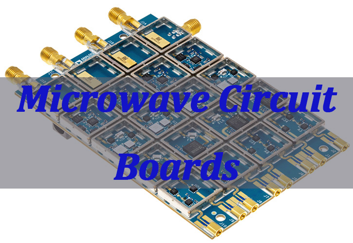
Microwave circuit boards are the specialized backbone of modern high-frequency electronics, enabling the transmission and processing of signals in the GHz to tens of GHz range. This article delves into the design, manufacturing, and material intricacies of these critical components, providing a comprehensive guide for engineers and procurement specialists navigating the RF and microwave PCB landscape.
Developing a successful high-frequency product is fraught with challenges. What Are Key Performance Challenges in RF and Microwave Printed Circuit Boards for Multi-GHz Systems?
Signal Degradation & Loss: Excessive insertion loss and poor signal integrity at target frequencies, rendering the system inefficient or non-functional.
Impedance Mismatch & Reflections: Inconsistent dielectric constants and imprecise trace geometries causing signal reflections, standing waves, and degraded power transfer.
Thermal Management Failures: Inadequate material selection or design leading to overheating, delamination, and permanent performance drift in active circuits.
Prototype-to-Production Inconsistency: Performance metrics that are achievable in the lab but cannot be reliably replicated in volume manufacturing due to process variability.
Cost and Timeline Overruns: Unforeseen manufacturing complexities, material waste, and multiple prototype spins that blow budgets and miss critical market windows.
Overcoming these hurdles requires a manufacturer with deep domain expertise and a holistic approach. A premier microwave circuit board manufacturer like BEST Technology addresses these core issues directly.
Advanced Material & Process Mastery: Utilizing low-loss, thermally stable substrates and controlled processes to minimize Df and ensure consistent Er, directly combating signal loss.
Precision Engineering & DFM: Implementing strict impedance control with tight tolerances on trace width, spacing, and copper profile to eliminate mismatches and reflections.
Integrated Thermal Design Support: Recommending and processing materials with optimal thermal conductivity and designing for efficient heat dissipation from the outset.
Design for Manufacturing (DFM) Review: Providing expert, early-stage DFM analysis to ensure designs are not only functional but also manufacturable and scalable with high yield.
Streamlined Turnkey Project Management: Offering a complete microwave circuit board factory service—from material procurement to assembly—under one roof, ensuring control, faster turnaround, and predictable costing.
BEST Technology is a premier China microwave circuit board manufacturer specializing in high-frequency, high-reliability PCBs. Our expertise lies in delivering full turnkey solutions for complex RF and microwave projects, combining state-of-the-art manufacturing with rigorous testing to ensure your designs perform as intended, from prototype to volume production. For your next project, pls feel free to contact us at sales@bestpcbs.com.
What Are Microwave Circuit Boards?
Microwave circuit boards, often referred to as RF and microwave printed circuit boards, are a specialized class of PCBs designed to operate at frequencies typically ranging from about 300 MHz up to 100 GHz and beyond.
Unlike standard digital boards, their primary function is to guide, manipulate, and process electromagnetic waves with minimal loss and distortion. Their performance is critically dependent on the board’s material properties and physical geometry.
How Does Microwave Circuit Board Design Differ From Standard RF and Digital PCB Layouts?
Microwave PCB design transitions from considering signals as simple voltage changes to managing them as electromagnetic waves traveling across a transmission line. This paradigm shift introduces several critical design disciplines not found in lower-frequency layouts. The focus moves from mere connectivity to controlling the electromagnetic field itself.
Transmission Line Theory is Paramount: Every trace is a controlled-impedance transmission line (microstrip, stripline, coplanar waveguide). Its dimensions must be meticulously calculated based on the substrate’s dielectric constant (Dk) at the target frequency.
Parasitics Are Performance-Killers: Stray inductance and capacitance from vias, bends, and component pads can no longer be ignored. They must be modeled, minimized, or incorporated into the design as functional elements.
Material Properties Dictate Design: The dielectric constant (Dk) and its consistency, as well as the dissipation factor (Df), are first-order design inputs, not afterthoughts. Design starts with material selection.
EM Simulation is Non-Optional: Extensive 3D electromagnetic field simulation is required to predict and optimize S-parameters (e.g., S11 for return loss, S21 for insertion loss) before fabrication.
Grounding and Shielding are Critical: Preventing radiation loss, crosstalk, and mode conversion requires continuous, low-inductance ground planes and thoughtful cavity isolation.
In essence, microwave circuit board design is an exercise in electromagnetic integrity, where the interplay between physics, materials, and geometry determines success or failure.
Why Manufacturing Precision Matters When Working With Microwave Printed Circuit Boards?
At microwave frequencies, the wavelength of the signal becomes comparable to the physical dimensions of the PCB features. Minor manufacturing variances that are negligible at lower frequencies can cause catastrophic performance shifts. Precision is not a luxury; it is the foundation of functionality.
Impedance Control: A ±10% variation in trace width or dielectric thickness can lead to a significant impedance mismatch, causing reflections (high VSWR) and reducing power delivered to the load.
Surface Roughness: Excessive copper foil roughness increases conductor loss, as the signal propagation concentrates near the conductor surface (skin effect). Smoother copper is essential for low-loss performance.
Dielectric Constant (Dk) Tolerance: Inconsistent Dk across a panel or from batch to batch alters the electrical length and phase of signals, ruining the performance of filters, phase arrays, and couplers.
Registration and Alignment: Misalignment between layers in multilayer boards changes the effective geometry of controlled impedance lines and can short or couple unintended elements.
Manufacturing Variance
Potential Impact at Microwave Frequencies
Trace Width Tolerance ±15%
Impedance deviation, degraded return loss (S11)
Dielectric Thickness Variation
Changed phase & impedance, filter frequency shift
Poor Etch Profile (Trapezoidal)
Increased loss, impedance inaccuracy
Laminate Dk Tolerance ±0.5
Shift in electrical length, disrupted timing/phase
Therefore, partnering with a microwave printed circuit boards factory in China like BEST Technology, which maintains tight process controls, is crucial for predictable, high-performance outcomes.
Which Microwave Circuit Board Material Options Support Stable Performance at GHz Frequencies?
The choice of substrate material is the first and most critical decision in microwave printed circuit board design. Ideal materials provide stable electrical properties, low loss, and consistent manufacturability across the required frequency and temperature range.
PTFE-Based Laminates (e.g., Rogers RO4000® Series, Taconic RF-35): The industry standard for high-performance. They offer extremely low dissipation loss (low Df), stable Dk over frequency/temperature, and low moisture absorption. Ideal for critical circuits like antennas and filters.
Hydrocarbon Ceramic Filled (e.g., Rogers RO3000® Series): Excellent electrical performance with a lower cost profile than pure PTFE. They provide good thermal conductivity for heat dissipation and are suitable for a wide range of applications.
Polyphenylene Oxide (PPO)-Based Materials: Offer a balance of performance and cost, with stable Dk and lower loss than standard FR-4, often used in automotive radar and telecom infrastructure.
Standard FR-4: Not recommended for core microwave functions above 1-2 GHz due to its high and variable Df, inconsistent Dk, and significant loss tangent. It may be used in mixed-signal boards for the digital sections only.
How Are Microwave Circuit Boards Used in High-Frequency Applications?
Microwave circuit boards are enabling technologies across industries that demand high-speed wireless communication, sensing, and data processing.
Aerospace & Defense: Phased array radars, electronic warfare (EW) systems, satellite communication (SATCOM) terminals, and missile guidance systems.
Telecommunications: 5G/6G base station antennas and power amplifiers, microwave backhaul links, and millimeter-wave equipment.
Automotive: Advanced Driver-Assistance Systems (ADAS), including radar sensors (77 GHz) for collision avoidance and adaptive cruise control.
Medical & Scientific: MRI systems, radiation therapy equipment, and high-frequency test & measurement instrumentation like network analyzers.
Cost Factors That Influence Microwave Circuit Board Price From Prototype to Volume Production
The microwave circuit board price is influenced by several key factors beyond standard PCB costing.
Substrate Material: Specialty microwave laminates (e.g., Rogers, Taconic) are significantly more expensive than FR-4.
Layer Count and Complexity: More layers and hybrid constructions (mixing different materials) add cost and processing difficulty.
Tolerances and Feature Size: Tighter impedance control, finer lines/spaces, and smaller via sizes require advanced equipment and processes, increasing cost.
Testing and Certification: Extensive RF testing (e.g., net analyzer testing), impedance testing, and industry-specific certifications (e.g., ISO, AS9100) add to the cost but are essential for quality assurance.
Order Volume: Unit cost decreases with higher volumes due to amortized setup and tooling costs, but material cost remains a dominant factor.
How to Select Reliable Best HDI PCB Manufacturers for RF and Microwave Circuit Boards?
Choosing the right partner is critical. Look for manufacturers that demonstrate proven expertise, not just capability. The best HDI PCB manufacturers for RF and microwave circuit boards will exhibit the following:
Proven High-Frequency Portfolio: Request and review case studies or sample reports of previous work in your target frequency band.
Material Expertise & Partnerships: They should have deep knowledge of and reliable supply chains for premium laminate suppliers.
Advanced Process Controls: Inquire about their controls for impedance, etch compensation, lamination, and plating specifically for RF boards.
In-House RF Testing Capability: The ability to perform basic S-parameter or impedance testing in-house is a strong indicator of serious commitment to the RF market.
Engineering Support: They should offer proactive microwave circuit board design review (DFM) to catch issues before fabrication begins.
Why is EBest Circuit (Best Technology) Considered a Premier Microwave Circuit Board Manufacturer for Complex RF Projects?
EBest Circuit (Best Technology) has solidified its reputation as a leading microwave and RF circuit board manufacturer by combining nearly two decades of specialized experience with robust manufacturing capabilities and an unwavering commitment to quality.
1. Proven Experience and Scale:
19 Years of Focused Expertise: Founded in 2006, we possess 19 years of deep industry knowledge in advanced PCB manufacturing, specifically catering to the demands of high-frequency applications.
Significant Production Capacity: Our factory boasts a monthly production capability of 260,000 square feet (28,900 square meters), handling over 1,000 different boards monthly. This scale ensures we can manage both prototype and mass production needs reliably.
Global Client Trust: We have successfully served 1,700+ satisfied clients across 40+ countries, demonstrating our ability to meet international standards and project requirements.
2. Specialized Material and Manufacturing Capabilities for RF/Microwave:
Our technical specifications, as detailed in our capability charts, are precisely aligned with the needs of RF and microwave boards:
High-Frequency Materials: We are highly experienced in processing specialized laminates critical for RF performance, including Rogers (4003, 4350, 5880), Taconic, and Isola high-speed materials (e.g., FR408HR). We also offer high-Tg FR4 (up to TG >180) for demanding applications.
Precision Engineering: We achieve fine lines and spaces down to 3/3 mil (0.075/0.075mm) for standard processes and 2/2 mil (0.05/0.05mm) for HDI, which is essential for controlling impedance in high-frequency designs.
Advanced Layer and Thickness Control: We manufacture multi-layer boards up to 32 layers, accommodating complex RF circuit architectures with controlled impedance tolerances of ±10% (>50 ohm) or ±5 ohm (≤50 ohm).
3. Certified Quality Assurance and Rigorous Testing:
Quality is non-negotiable in RF projects. Our commitment is validated by:
International Certifications: We hold ISO9001:2015 for quality management and IATF 16949:2016 for automotive quality, underscoring our process discipline. Additionally, we are ISO 13485:2016 certified for medical devices and compliant with RoHS and REACH environmental standards.
Comprehensive Testing Regime: Our facility is equipped with advanced test equipment like Automatic Optical Inspection (AOI), X-Ray copper thickness testers, Flying Probe Testers, and Micro-section Analysis systems to ensure every board meets stringent quality criteria for signal integrity and reliability.
4. Full Turnkey Solution with Unmatched Speed and Support:
We simplify the supply chain for our clients, providing a seamless journey from concept to final product.
True One-Stop Service: Our services encompass PCB design, fabrication, component sourcing, PCB assembly (SMT & THT), and full box-build integration.
Rapid Prototyping: We understand the iterative nature of RF design. We offer expedited services, with urgent FR4 prototypes (1-8 layers) shipping in as fast as 24 to 72 hours.
Reliable Delivery: We maintain an On-Time Delivery rate of 97%, ensuring your project timelines are met without compromise.
By integrating deep technical expertise, transparent and verifiable capabilities, and a quality-centric culture, EBest Circuit (Best Technology) provides the essential foundation for success in complex microwave and RF projects. We don’t just make boards; we deliver reliable, high-performance solutions backed by data and decades of experience.
To wrap up, microwave circuit boards are the critical, high-performance platforms that make advanced wireless and sensing technologies possible. This guide has explored their unique design requirements, material science, manufacturing imperatives, and application landscapes. BEST Technology stands ready as your full-service partner, offering the material knowledge, precision engineering, and manufacturing excellence needed to bring your most ambitious RF and microwave projects to life with speed. For more information or if you would like to send us any inquiry, please send us an email through the contact form at the bottom of our Contact Page.
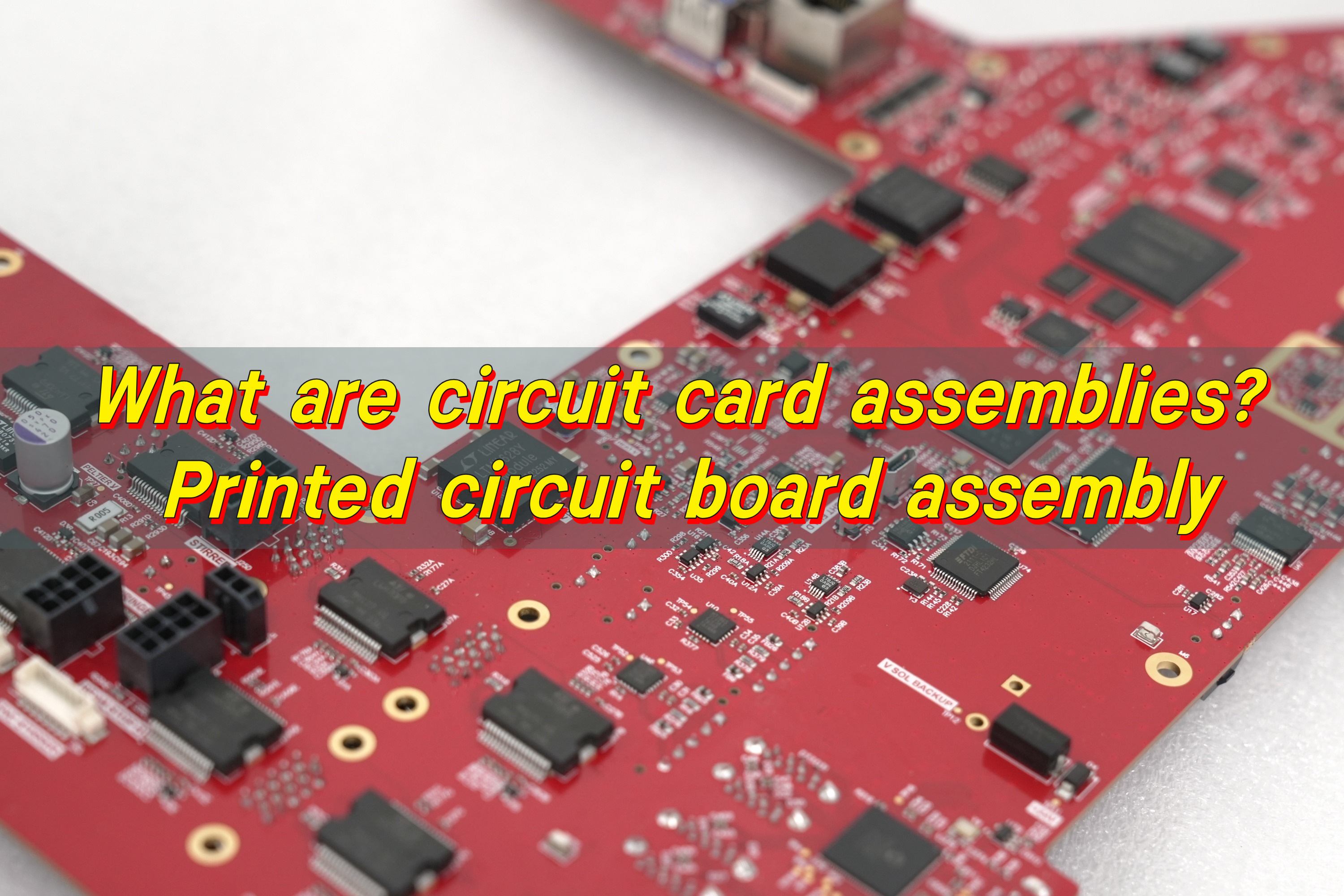
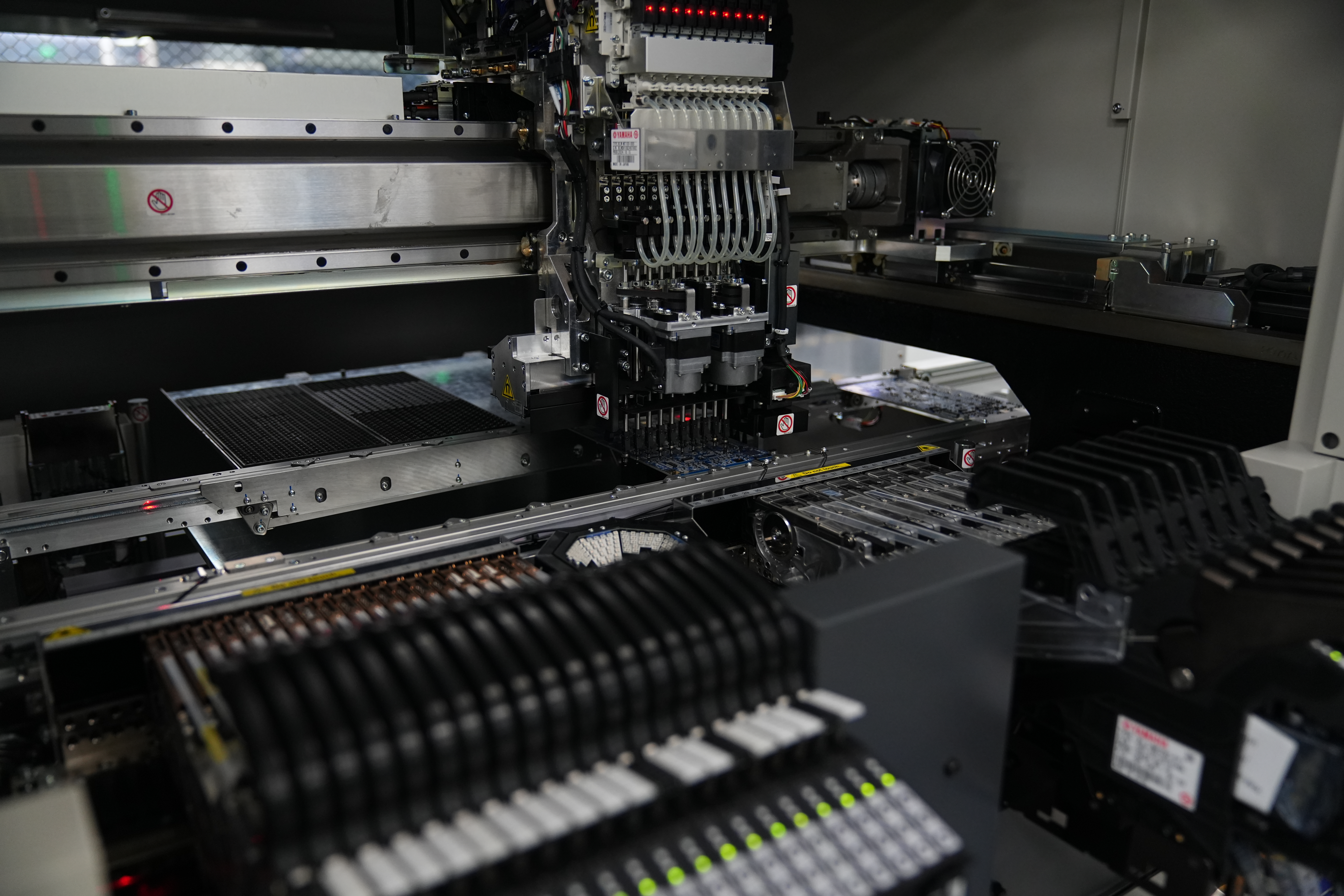
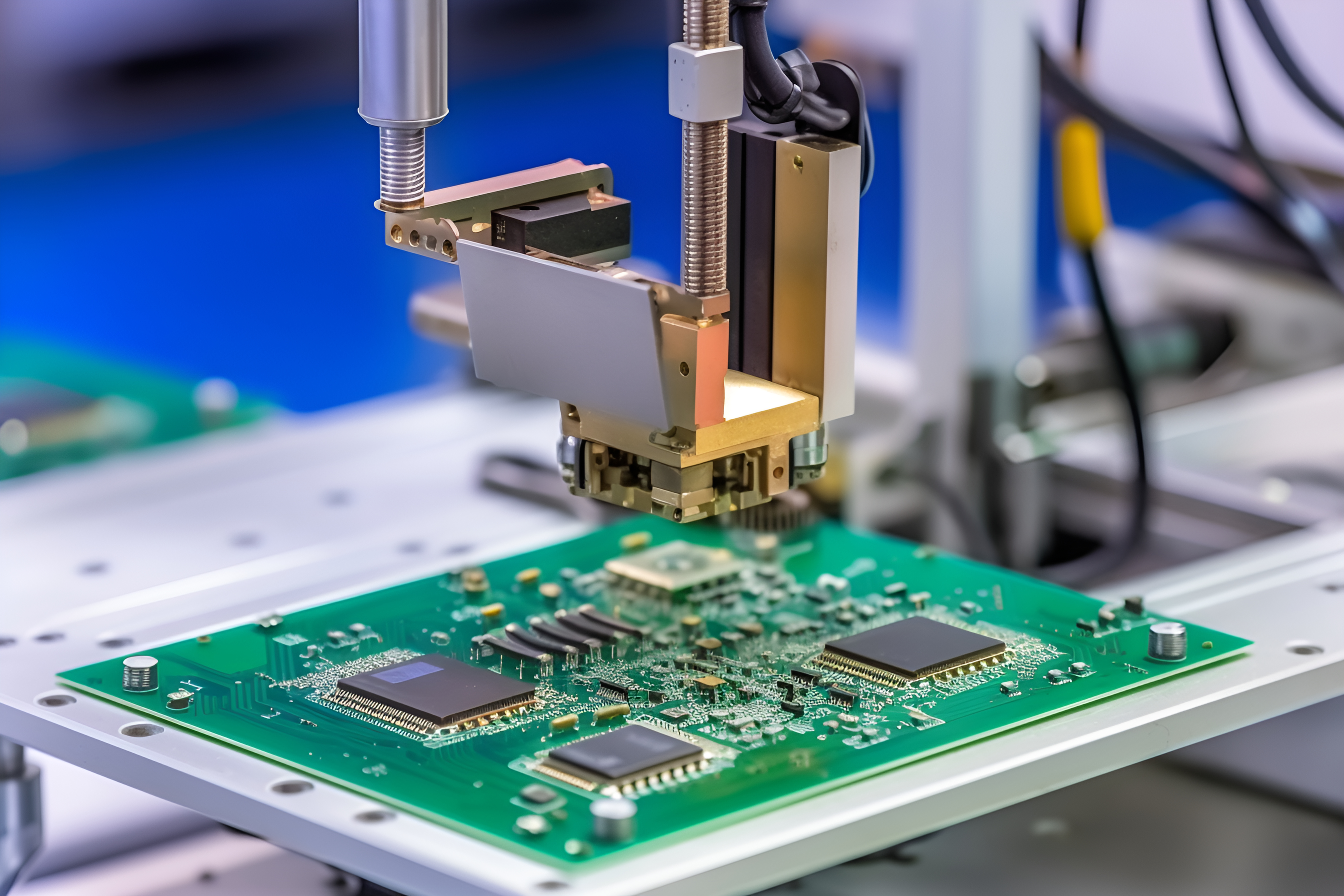
Circuit card assemblies sit at the core of modern electronics. A circuit card assembly is a printed circuit board that has been fully populated with electronic components and soldered into place. Once assembled, it becomes a working unit capable of controlling power, processing signals, and enabling communication within an electronic device.
What Is a Circuit Card Assembly?
A circuit card assembly, often shortened to CCA, is a printed circuit board that has electronic components mounted and connected to it. These components are not loose. They are fixed, soldered, and electrically linked according to a design.
The circuit card assembly definition focuses on function. It is not just a board with copper paths. It is a working electronic unit. Once assembled, it can process signals, control power, or manage data.
Many people use the term printed circuit board assembly in the same way. In daily use, they often mean the same thing. Still, some industries prefer “circuit card assembly” because it highlights the complete, functional state.
A bare board cannot do anything alone. A circuit card assembly can. This is why CCAs are central to electronics manufacturing.
What Are the Main Components of a Circuit Card Assembly?
A circuit card assembly is a system. Every part plays a role. Each component adds a specific function, and together they create reliable operation.
The Printed Circuit Board: The printed circuit board is the foundation. It is usually made from fiberglass material like FR-4. Copper layers form electrical paths on the surface or inside the board. The board provides structure. It also controls signal flow.
Passive Components: Passive parts include resistors, capacitors, and inductors. These components shape current and voltage. They store energy, limit flow, or filter noise.
Active Components: Active components bring intelligence. These include microcontrollers, processors, and integrated circuits. They process signals. They make decisions. They control outputs.
Connectors and Interfaces: Connectors link the assembly to other systems. They allow power input, data transfer, or mechanical connection.
Solder Materials: solder joints connect everything. The quality of solder paste, reflow profile, and inspection determines long-term stability. A strong joint survives vibration and heat.
Each component matters. Together, they turn a simple board into a reliable circuit card assembly.
What Are the Different Types of CCA Assembly?
Different products need different assembly styles. Choosing the right type affects cost, size, and performance.
Through-Hole Assembly
Through-hole assembly uses components with long leads. These leads pass through holes in the board and are soldered on the opposite side.
This method offers strong mechanical bonds. It works well for large components and connectors. However, it takes more space. It also increases labor.
Surface Mount Assembly
Surface mount technology places components directly onto the board surface. No holes are needed for most parts.
This approach allows higher density. Boards can be smaller and lighter. Most modern printed circuit board assembly manufacturers focus on this method. It suits automation and high-volume production.
Mixed Technology Assembly
Some assemblies combine both methods. Sensitive or heavy parts may use through-hole, while smaller parts use surface mount.
Prototype Printed Circuit Board Assembly
Prototype assembly focuses on early design stages. Volumes are low. Speed matters more than cost. This type supports testing and refinement. Many printed circuit board assembly services specialize in fast prototype builds.
Each type serves a purpose. The best choice depends on product goals, budget, and lifecycle.
How Does a Circuit Card Work?
A circuit card assembly works by guiding electrical signals along designed paths. These paths connect components in a precise sequence.
Power enters through a connector or contact. It flows through regulators and filters. These parts stabilize voltage.
Signals then move into active components. Processors read inputs. Logic circuits decide actions. Outputs leave the board through connectors, displays, or motors. Signal integrity matters. Layout matters.
Even small design choices affect performance. Trace width, spacing, and grounding all play roles. A circuit card does not act alone. It interacts with firmware, mechanical housing, and external systems.
What Does a Circuit Card Assembly Do?
A circuit card assembly acts as the control center of an electronic device. It manages power, data, and interaction.
In some products, it handles simple switching. In others, it runs complex software. Its job is to turn input into output. Buttons become actions. Sensors become data. Signals become results.
A well-built assembly delivers stable performance. It handles heat. It resists vibration. It lasts for years.
What Are Circuit Card Assemblies Used For?
Circuit card assemblies appear almost everywhere. If a device uses electricity, it likely includes one.
Consumer Electronics: Phones, laptops, and wearables rely on compact assemblies. Surface mount printed circuit assembly manufacturing supports this demand.
Industrial Equipment: Factories use assemblies for control systems and automation. These environments demand durability.
Medical Devices: Medical equipment depends on accuracy and safety. Circuit card assemblies control imaging, monitoring, and diagnostics. Quality standards are strict. Traceability matters.
Automotive Systems: Vehicles contain dozens of assemblies. They manage engines, safety systems, and infotainment. Temperature resistance and long life are critical.
Communication Systems: Routers, base stations, and networking gear rely on high-speed assemblies. Signal integrity and layout design play major roles.
What Is the Difference Between Circuit Card Assembly and PCB Assembly?
This question comes up often. The terms are closely related, yet they emphasize different stages.
A printed circuit board is the bare board. It has copper traces and holes, but no components.
A printed circuit board assembly includes components mounted and soldered. It is functional.
A circuit card assembly usually refers to the same assembled board. The term highlights readiness for use.
In many industries, people use these terms interchangeably. Still, “circuit card assembly” often appears in defense, aerospace, and industrial sectors.
What Are the Applications of Circuit Board Assemblies?
Circuit board assemblies support modern life. Their applications keep expanding as technology evolves.
They power smart homes.
They control renewable energy systems.
They drive automation.
They support innovation.
As demand grows, so does the need for skilled manufacturers. Printed circuit board assembly manufacturers now offer advanced inspection, testing, and box build options. Box build printed circuit board assembly services go even further. They deliver complete systems, not just boards.
In global markets, China printed circuit board assembly plays a key role. Scale, experience, and supply chain strength support competitive production. With long-term manufacturing experience and a mature supply chain, BEST Technology combines regional strengths with consistent quality control, supporting both high-mix projects and volume production.
Conclusion:
A circuit card assembly is a fully populated and functional electronic board. It combines a printed circuit board with mounted components to create real performance. From consumer electronics to industrial systems, these assemblies power modern life.
For professional printed circuit board assembly services and reliable manufacturing support, contact our team at sales@bestpcbs.com
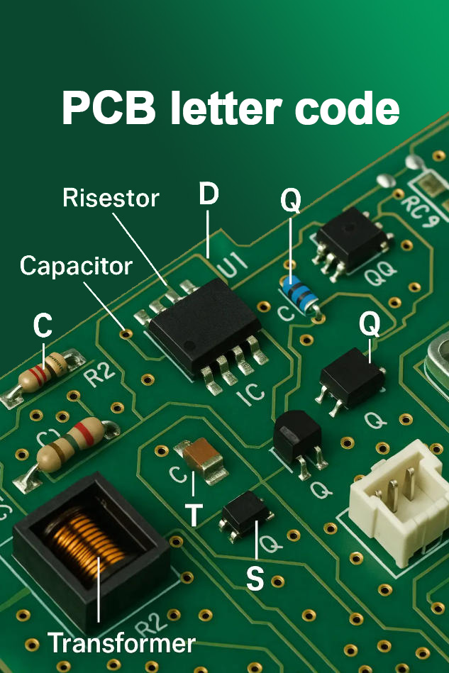
What Are PCB Letter Codes? — Definitions & Core Functions
PCB letter codes are essential identifiers used in printed circuit board (PCB) design and manufacturing, serving as a universal language to label components, layers, test points, and functional zones on a board. These PCB letter codes eliminate confusion during assembly, repair, and quality control, ensuring that engineers, technicians, and suppliers across the globe can quickly interpret a PCB’s layout and purpose. Whether you’re designing a new board, troubleshooting a faulty circuit, or sourcing replacement parts, understanding PCB letter codes is non-negotiable for streamlining processes and avoiding costly errors. Without clear, standardized letter codes, even simple tasks like identifying a resistor or navigating a multi-layer PCB would become time-consuming and error-prone.
International Standards & Design Specifications for PCB Letter Codes (IEEE/IPC Standards Explained)
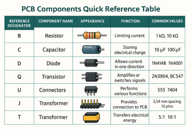
When working with PCB letter codes, adherence to international standards is critical to ensure compatibility and clarity. The two most widely recognized standards are IEEE (Institute of Electrical and Electronics Engineers) and IPC (Association Connecting Electronics Industries), each outlining guidelines for consistent PCB letter codes usage. IEEE standards, such as IEEE 315, focus on component labeling conventions, while IPC standards like IPC-2221 detail general PCB design requirements, including letter code formatting for layers and test points. Following these standards ensures that your PCB letter codes are understandable to anyone working with the board, regardless of their location or industry. For example, IPC specifies that power-related components should use letter codes starting with “P” (e.g., P1 for Power Connector), while IEEE mandates that resistors use “R” (e.g., R12 for Resistor 12). Ignoring these standards can lead to miscommunication, delayed projects, and incompatible components.
pcb code list (Comprehensive Common PCB Letter Codes Reference Table)
Having a reliable reference for common PCB letter codes saves time and reduces guesswork. Below is a complete, industry-aligned list of PCB letter codes (per IEEE 315 and IPC-2221 standards), covering passive components, active components, connectors, power elements, test points, and specialized parts:
This comprehensive PCB letter codes list covers 95% of components used in consumer electronics, industrial equipment, automotive PCBs, medical devices, and aerospace applications. For ultra-specialized use cases (e.g., military-grade PCBs), additional industry-specific codes may apply, but this table serves as the definitive reference for standard PCB design and manufacturing workflows.
pcb components identification (PCB Component Identification: Quick Mapping from Codes to Physical Parts)
Translating PCB letter codes to physical components requires a combination of visual inspection and basic knowledge of component types. Start by locating the printed letter code on the PCB—this is typically printed near the component itself. Next, cross-reference the code with the list above to identify the component category (e.g., “C” for capacitor). Then, use physical characteristics to confirm: resistors are often cylindrical or rectangular with color bands, capacitors are small and cylindrical or rectangular, and ICs are larger with multiple pins. For example, if you see “U06” on the board, you’ll know to look for a multi-pin integrated circuit nearby. This PCB components identification process becomes faster with practice, but having a cheat sheet of PCB letter codes and component shapes will accelerate your workflow. For hard-to-identify components, use a digital multimeter to test functionality, which can confirm if a component matches its labeled code.
Numbering Rules for PCB Letter Codes (Sequential Numbering, Zonal Numbering, Multi-layer Board Numbering)
PCB letter codes aren’t just random labels—they follow specific numbering rules to ensure organization and scalability. The three most common numbering systems are:
Sequential Numbering: This is the simplest method, where components are numbered in the order they’re placed on the PCB (e.g., R01, R02, R03…). It’s ideal for small, simple PCBs with few components.
Zonal Numbering: For larger PCBs, components are grouped by zone (e.g., top-left, power section) and numbered within each zone (e.g., R101 for Resistor in Zone 1, Position 1; R205 for Resistor in Zone 2, Position 5). This makes it easier to locate components in complex layouts.
Multi-layer Board Numbering: Multi-layer PCBs add a layer identifier to the code (e.g., R3-09 for Resistor on Layer 3, Position 9). This is critical for distinguishing components on different layers, which is essential during assembly and repair.
Understanding these PCB letter codes numbering rules helps you navigate any PCB design, whether it’s a small hobby board or a large industrial PCB. Consistency in numbering also ensures that your PCB letter codes are compatible with CAD software and manufacturing processes.
Detailed Explanation of Special-Function PCB Letter Codes (Power Supply, Test Points, Interface Codes)
Beyond standard component labels, PCB letter codes include special-function codes for critical board features. These codes are designed to highlight important areas and simplify maintenance:
Power Supply Codes: These start with “P” (e.g., P3V3 for 3.3V Power Rail, P5V for 5V Power Rail) and indicate voltage levels or power distribution points. They’re vital for avoiding short circuits and ensuring proper power delivery.
Test Point Codes: Labeled with “TP” (e.g., TP_VIN for Input Voltage Test Point, TP_GND for Ground Test Point), these codes mark points where technicians can measure signals or voltages during testing. They eliminate the need to probe sensitive components directly.
Interface Codes: These identify external connections, such as “USB1” for USB Port 1, “ETH0” for Ethernet Port 0, or “HDMI2” for HDMI Port 2. They make it easy to map external devices to the PCB’s internal circuitry.
Mastering these special-function PCB letter codes is key for anyone involved in PCB testing, repair, or system integration. They reduce the risk of mistakes and make complex boards more manageable.
Recommended Practical Tools & Resources for Decoding PCB Letter Codes
Decoding PCB letter codes becomes even easier with the right tools and resources. Here are our top recommendations for both beginners and professionals:
Digital Multimeters: A basic multimeter can test components (e.g., resistors, capacitors) to confirm their identity, complementing the letter code label.
PCB CAD Software: Tools like Altium Designer, KiCad, or Eagle include built-in PCB letter codes libraries and validation features to ensure compliance with standards.
Online Databases: Websites like IPC’s standards library or IEEE Xplore provide access to official PCB letter codes specifications for advanced users.
Mobile Apps: Apps like “PCB Component Identifier” or “Electronics Reference” offer on-the-go access to PCB letter codes lists and component identification guides.
These tools streamline the process of working with PCB letter codes, whether you’re in the office, workshop, or field. Investing in reliable resources will save you time and improve the accuracy of your work.
3 Core Tips for Beginners to Master PCB Letter Codes Quickly
If you’re new to PCB letter codes, these three tips will help you master them in no time:
Memorize High-Frequency Codes: Start by learning the most common codes (R, C, D, U, J) since they appear on nearly every PCB. Write them down or use flashcards for quick recall.
Practice with Real PCBs: Grab old electronics (e.g., smartphones, routers) and identify components using their PCB letter codes. This hands-on practice is far more effective than just reading lists.
Stick to Standards: Always reference IEEE or IPC standards when working with PCB letter codes. Avoid creating custom codes unless absolutely necessary, as this can cause confusion for others.
By focusing on these fundamentals, you’ll build confidence and proficiency with PCB letter codes in weeks, not months.
Application Cases of PCB Letter Codes in Different Scenarios (Repair, Design, Procurement)
PCB letter codes are versatile and used across multiple stages of the PCB lifecycle. Here are real-world examples of how they’re applied:
Repair: A technician troubleshooting a faulty TV PCB sees the code “Q04” near a burnt component. Using the PCB letter codes list, they identify it as a transistor, source a replacement, and fix the issue in minutes.
Design: An engineer designing a medical device PCB uses zonal numbering for PCB letter codes (e.g., R302 for Resistor in the Sensor Zone). This helps the assembly team quickly locate components and ensures compliance with regulatory standards.
Procurement: A buyer sourcing components for a production run references the PCB letter codes on the bill of materials (BOM) to order the correct resistors (R01-R50) and capacitors (C01-C35). This eliminates ordering errors and delays.
In each scenario, PCB letter codes improve efficiency, reduce mistakes, and ensure clear communication between teams.
Common Misunderstandings & Pitfalls of PCB Letter Codes
Even experienced professionals can fall prey to misunderstandings when working with PCB letter codes. Here are the most common pitfalls to avoid:
Ignoring Standard Differences: Assuming IEEE and IPC PCB letter codes are identical is a mistake. For example, some IPC codes for test points differ from IEEE, so always confirm which standard the PCB uses.
Custom Code Overload: Creating too many custom PCB letter codes for specialized components can make the board unreadable to others. Use custom codes sparingly and document them clearly.
Poor Placement: Printing PCB letter codes too close to components or in hard-to-see areas (e.g., under large ICs) makes them useless. Ensure codes are visible and easily accessible.
Inconsistent Numbering: Mixing sequential and zonal numbering on the same PCB causes confusion. Stick to one system throughout the design.
By avoiding these pitfalls, you’ll ensure that your PCB letter codes are effective and user-friendly.
FAQ: Frequently Asked Questions About PCB Letter Codes
Q1: Do different manufacturers use different PCB letter codes?
A1: While most manufacturers follow IEEE or IPC standards for PCB letter codes, some may use custom variations for specialized products. Always check the PCB’s datasheet or consult the manufacturer if you encounter unfamiliar codes.
Q2: What’s the difference between PCB letter codes for single-layer and multi-layer boards?
A2: Multi-layer boards add a layer identifier to PCB letter codes (e.g., R2-07 for Layer 2, Resistor 7), while single-layer boards use simple sequential or zonal numbering. This layer distinction is critical for assembly and repair.
Q3: I can’t find a matching component for a PCB letter code—what should I do?
A3: First, confirm the standard (IEEE/IPC) used for the PCB letter codes. If the code is still unrecognizable, check the PCB’s BOM or contact the original equipment manufacturer (OEM) for clarification. You can also use a component tester to identify the part’s function.
Q4: Can I create my own PCB letter codes for a custom project?
A4: You can, but it’s not recommended unless the project is for personal use. Custom PCB letter codes can cause confusion for anyone else working on the board. If you must use custom codes, document them clearly and share the reference with your team.
Q5: Are PCB letter codes required for small hobby PCBs?
A5: They’re not mandatory, but using PCB letter codes on hobby PCBs is a good practice. It makes assembly easier, helps with troubleshooting, and prepares you for professional projects where codes are standard.
Q6: How do I handle conflicting PCB letter codes on a board?
A6: Conflicting codes (e.g., two components labeled “R05”) usually indicate a design error. Cross-reference the PCB with the BOM to confirm the correct labels, and contact the designer or manufacturer to resolve the issue before proceeding with assembly or repair.
Conclusion: Efficient Application Methodology for PCB Letter Codes
PCB letter codes are the backbone of clear communication in PCB design, manufacturing, and maintenance. By understanding their definitions, following international standards, using practical tools, and learning from real-world applications, you can leverage PCB letter codes to streamline your workflow, reduce errors, and improve collaboration. Whether you’re a beginner or a seasoned professional, mastering these codes is essential for success in the electronics industry.
If you’re in need of high-quality PCBs with accurate, standardized PCB letter codes that meet IEEE and IPC standards, look no further. We specialize in manufacturing custom PCBs tailored to your specific needs, with clear PCB letter codes that simplify assembly, repair, and compliance. Don’t let confusing or inconsistent codes slow down your project—place your order today by emailing us at sales@bestpcbs.com. Our team is ready to deliver reliable, industry-compliant PCBs that meet your deadlines and exceed your expectations.
Looking for PCB manufacturer in Bangladesh? This guide clarifies key aspects of collaborating with PCB manufacturer in Bangladesh, from identifying pain points to selecting partners and ensuring smooth project execution.
Bangladesh’s booming electronics industry has spurred strong demand for high-quality PCB (Printed Circuit Board) solutions. As PCB Manufacturer in Bangladesh continue to enhance their capabilities, local and international businesses alike are seeking reliable partners for their production needs. Navigating this market, however, is challenging due to varying expertise, production standards, and service quality across providers.
Are You Facing These Problems?
Excessive Prototyping Costs: Many businesses encounter unexpected fees after initial low-cost prototyping quotes, with some PCB manufacturers in Bangladesh hiking prices for adjustments or small-batch production.
Lack of Design Support: Limited local expertise in PCB design optimization leads to design flaws that only surface during production, causing delays and rework.
Inconsistent Production Quality: Disparities in material sourcing and quality control result in inconsistent PCB performance, even from the same manufacturer.
Unreliable Delivery Schedules: Frequent delays due to poor supply chain management or overpromising, disrupting downstream production plans.
Compliance and Certification Gaps: Difficulty verifying the authenticity of certifications (such as BSTI, BTRC) claimed by some local manufacturers, risking regulatory issues.
Our Solutions to These Problems
As a professional 19 years’ global PCB manufacturer, EBest Circuit (Best Technology) can provide you the following service and solutions to these problems:
No More Prototyping Cost Shocks: We quote prototyping upfront with a “Price Lock Guarantee”—the 5-piece $8 prototype quote you get is the final price, no hidden fees for adjustments or small batches. This cuts unexpected costs by 100% and keeps your budget on track.
Free DFM Support That Prevents Rework: Our 20+ senior engineers (with TI/Intel experience) run a free DFM (Design for Manufacturability) check on your files within 24 hours. We fix layout flaws, optimize signal paths, and flag compatibility issues, reducing rework by 90% vs. local competitors.
Consistent Quality, Every Batch: We use A-grade FR4 substrates (sourced from Japan) and imported Taiwanese AOI testers. Our QA team checks 100% of PCBs for shorts, opens, and dimensional errors, delivering a 95% yield rate, far above Bangladesh’s 82% average.
99.2% On-Time Delivery Rate: We avoid delays with a dual supplier network for raw materials and real-time production tracking. If we miss the agreed delivery date (e.g., 7 days for 4-layer PCBs), we cover 5% of the order value as compensation, no excuses, just accountability.
Certifications You Can Verify Instantly: We provide ISO 9001, ISO 13485, IATF 16949 certificates with live links to certification bodies’ databases. No more chasing fake docs, you can confirm validity in 2 minutes, ensuring compliance for EU/US exports.
Why Choose EBest Circuit (Best Technology) for Global PCB Manufacturer?
Reasons Why Choose EBest Circuit (Best Technology) for Global PCB Manufacturer:
Design Cost Optimization: Scalable Solutions for Mass Production Efficiency: We provide volume-oriented cost optimization suggestions for engineers’ PCB designs—such as precise adjustments to trace width/spacing to reduce copper usage and optimized via placement to minimize drilling waste. This has helped clients achieve an average 12% reduction in per-board costs, maximizing cost efficiency from prototype to mass production.
24-Hour Rapid Prototyping: Accelerating Project Timelines: Three dedicated emergency production lines enable same-day file confirmation and next-day sample delivery for 1-4 layer PCBs. This 24-hour turnaround is 3x faster than local competitors, ensuring project deadlines are met and accelerating prototype validation and market responsiveness.
99.2% On-Time Delivery: Reliable Supply Chain Performance: Dual-source material procurement and strict production scheduling achieve a 99.2% on-time delivery rate, exceeding the local industry average of 85%. Buyers can lock in delivery dates without buffer periods, preventing downstream production stoppages.
Batch-Wide Inspection: Zero-Defect Quality Assurance: 100% of mass production orders undergo AOI optical inspection and X-Ray scanning across all processes, from copper plating to profiling, with full quality records retained. The defect rate remains below 0.3%, providing engineers with reliable materials and eliminating prototype failure risks due to board issues.
Authoritative Certifications, Multi-Domain Compliance Assurance: Certifications include ISO 9001 (quality management), IATF 16949 (automotive), medical CE, and RoHS (environmental compliance). These cover high-end applications like automotive electronics and medical devices, allowing direct integration without additional compliance testing and speeding up product launches.
19 Years of Expertise: Rapid Technical Support: Specializing in PCB manufacturing for 19 years, our engineers are well-versed in design standards for telecom, consumer electronics, and other mainstream fields. Issues like impedance matching and signal interference are resolved within 2 hours, ensuring efficient technical problem-solving.
One-Stop Service: Three-Step Procurement: Integrating design optimization, prototyping, mass production, SMT assembly, and local logistics, the procurement process is streamlined into three steps: submit requirements, confirm samples, and receive final products. This reduces communication time by 60% compared to multi-vendor approaches.
Complimentary DFM Analysis: Proactive Design Risk Mitigation: Designers receive a free DFM manufacturability analysis report within 24 hours of submitting PCB files. The report identifies design flaws (e.g., overcrowded via placements causing pad cracking) and provides optimization solutions, helping 90% of new designers avoid mass production risks and improve first-pass design success rates.
Flexible Collaboration, Scalable Orders and Cost Stability: We support orders from 10-piece small batches to 50,000+ square meter monthly capacities. Long-term partners benefit from material price-lock agreements, mitigating global raw material price fluctuations and ensuring long-term procurement cost stability.
Welcome to contact us if you have any request for PCB design, prototyping, mass production and assembly: sales@bestpcbs.com.
1. Match technical capabilities to product needs: Automotive ECUs require 16-layer+ HDI boards while household fans only need 1-2 layer boards, so clarify the manufacturer’s process range. If the manufacturer claims to handle 0.2mm precision drilling, request the drilling test report from their Grameenphone OEM order as evidence.
2. Verify quality assurance with certificates and data: ISO13485 is mandatory for medical PCBs (such as Bangla Circuits’ certification) and TS16949 is required for automotive PCBs. Request the six-month defect rate report – the local industry average is 0.3%-0.5%, and leading enterprises like EBest Circuit (Best Technology) can achieve a rate as low as 0.01%.
3. Lock in delivery time with industry benchmarks and written agreements: The local average lead time is 3-7 days for prototyping and 8-12 days for mass production. For urgent orders, choose EBest Circuit (Best Technology) (24-hour prototyping) or Tech Circuit (4-6 day PCB delivery). Be sure to confirm in writing how compensation will be provided if mass production of 1,000 8-layer boards exceeds 8 days.
4. Focus on quotations and request details to avoid hidden costs: Ask for itemized quotations (FR-4 substrate accounts for 30%-40% of total costs) to avoid additional charges later – small factories often charge $50-$200 for design modifications. A reliable quotation should state that it is valid for 15 days and no extra fees will be charged for 2 minor modifications within 48 hours.
5. Refer to customer reviews and ask industry-specific questions: Startups can ask former customers of Dhaka Electronics about the minimum order quantity (MOQ) for their first small-batch order. Large enterprises can ask Rajshahi Circuit how they handled delays in 50,000-piece orders caused by material shortages. A 2024 local survey shows 90% of enterprises prioritize stable delivery over low prices.
6. Clarify after-sales service and finalize service commitments: Request a written agreement stating that defective products can be returned or exchanged within 7 days for quality issues, with the manufacturer covering shipping costs. Leading enterprises like Bangladesh Advanced PCBs provide 24-hour on-site support for major clients such as Maruti Suzuki, and ordinary clients should ensure a 4-hour phone response.
7. Test communication efficiency with a 3-day trial method: Send design files to request a DFM (Design for Manufacturability) report. A reliable manufacturer will provide feedback on trace width optimization suggestions within 24 hours. Prioritize partners with real-time WhatsApp communication and weekly email summaries of progress.
8. Choose the right location to save logistics costs and shorten lead time: For exports to India/Southeast Asia, select manufacturers near Chittagong Port such as Chittagong PCB Solutions to save 15%-20% on freight and reduce customs clearance time by 2-3 days. Local factories in Dhaka like Tech Circuit can achieve delivery within 1 day, avoiding 3-5 day delays from northern regions like Rangpur.
How to Evaluate the Production Capacity of PCB Manufacturing Company Bangladesh?
1. Check production scale with quantifiable indicators: Focus on three core dimensions when inquiring: factory area (manufacturers with scale usually have ≥5,000㎡ workshops), number of production lines (≥3 lines indicate stable capacity), and monthly output (≥20,000㎡ for mass production orders, ≥5,000㎡ for small-batch needs). Ask directly: “What is your monthly output of 8-layer PCBs? Can you provide a recent 3-month production report?”
2. Assess equipment quality by key parameters: Prioritize manufacturers with mainstream brand equipment: drilling machines (Hitachi, Makino) and AOI (Omron, Koh Young) are more reliable. Check equipment age (≤3 years is ideal) and quantity (e.g., ≥2 high-precision drilling machines for 0.2mm holes). Ask: “What is the brand and service life of your main etching and testing equipment? What is the monthly maintenance record?”
3. Evaluate workforce with structure and expertise: A reasonable workforce structure matters more than total numbers: technical engineers (PCB design, process) should account for ≥10% of the total staff, and skilled workers (solderers, inspectors) should have ≥2 years of experience. Inquire about training systems: “Do you have regular technical training? Are there cooperative programs with local technical colleges?”
4. Review past projects with industry matching: Request case materials of large orders completed in the past 6 months, such as 10,000-piece+ PCB contracts. Focus on two points: industry matching (e.g., if you make automotive PCBs, check if they have cooperated with local auto parts factories) and delivery data (on-time delivery rate ≥95% is qualified).
5. Check material inventory with risk resistance: Reliable manufacturers have inventory management systems: core substrates (FR-4) should have ≥30 days of stock, and key chemicals (etchants) have ≥15 days of reserve. Ask: “Do you use ERP to manage inventory? How many alternative suppliers do you have for copper foils?”
6. Inquire about production flexibility with response speed: Test their adaptability: “How long does it take to switch from 100-piece prototyping to 10,000-piece mass production?” (≤2 days is excellent). “What is the maximum number of design modifications you can accept within a week?” (≥3 times shows flexibility). Also confirm the minimum order quantity (MOQ ≤50 pieces is friendly for startups).
7. Evaluate quality control with process coverage: A complete QC system covers ≥5 key nodes: incoming material inspection (100% for substrates), in-process testing (etching thickness, hole position accuracy), and final inspection (functional testing). Ask: “What is your sampling inspection ratio for mass production? Do you follow the AQL 2.5 standard? What is the 6-month defect rate?” (Top manufacturers keep it ≤0.05%).
8. Check expansion plans with solid evidence: Manufacturers with growth potential have clear expansion schedules: ask if they have purchased new land, signed equipment procurement contracts, or recruited additional technical teams. For example, “Do you have plans to increase production capacity this year? What is the expected monthly output after expansion?” (≥50% growth indicates strong capacity).
How to Evaluate the Delivery Time of PCB Manufacturer in Bangladesh?
1. Get written, itemized delivery commitments Don’t accept verbal promises. Ask for a document stating: “1000pcs 8-layer PCBs: prototyping 3 days + mass production 7 days + Dhaka delivery 1 day = total 11 days”. Clearly note compensation (e.g., 5% order reduction per delayed day) for breaches.
2. Clarify delay response plans for common risks Directly ask three questions: 1. “How to handle substrate shortages?” (Qualified answer: 2+ alternative suppliers); 2. “What if there’s a power outage?” (Ideal: Backup generators ensuring 24h production); 3. “How to fix logistics delays?” (Example: Chittagong PCB Solutions uses port-side warehouses for fast rerouting).
3. Verify logistics partners and cost transparency: Ask for their regular courier list (prefer DHL, Sundarban Courier for reliability). Confirm: “Is the delivery fee included in the quote? Will there be extra charges for remote areas like Rangpur?”
4. Check delivery performance with 2+ client references. Contact their recent clients (e.g., for Rajshahi Circuit, ask auto parts factories): “What was their on-time delivery rate for your 50,000pcs order? How did they handle delays?” Aim for ≥95% on-time rate.
5. Confirm rush order options and costs upfront Inquire: “Can you expedite a 500pcs order? How fast?” (EBest Circuit (Best Technology) offers 12h rush); “What’s the premium?” (Industry standard: 30%-50% of original price, avoid vague “extra fees”).
6. Evaluate scheduling efficiency via system proof Ask: “Do you use ERP software for production scheduling?” Request a screenshot of your order’s scheduled nodes (e.g., “Material arrival: Day 1 → Etching: Day 2 → Inspection: Day 6”) to avoid bottlenecks.
7. Check contingency plans for critical links Focus on two points: 1. Material inventory (FR-4 stock ≥30 days is safe); 2. Production backup (e.g., Bangladesh Advanced PCBs has 1 spare etching line for emergencies).
8. Confirm real-time tracking methods Require accessible tracking: “Will I get a WhatsApp update when the order enters testing? Can I check progress via your online system?” Avoid manufacturers that only reply “it’s in production”.
Frequently Asked Questions About PCB Manufacturing in Bangladesh
Q1: My last PCB order was delayed by 10 days with no prior notice. How to avoid this? A1: Choose manufacturers that provide written delivery commitments (e.g., EBest Circuit (Best Technology)’s “1000pcs 8-layer PCBs: 8-day mass production + 1-day delivery” document). Require real-time tracking-Email updates for each production node (material arrival, etching, inspection).
Q2: I’m a startup needing 50 small-batch PCBs, but most factories refuse. Who accepts low MOQ? A2: Focus on manufacturers targeting SMEs, such as EBest Circuit (Best Technology) Co.,Ltd, which offers MOQ as low as 10 pieces. When inquiring, specify “50pcs 2-layer PCBs, 10cm×10cm” directly—reliable suppliers will quote within 2 hours, not just say “we don’t take small orders.”
Q3: The PCBs I received had solder defects, but the factory said it’s my assembly issue. How to define responsibility? A3: Prior to order, confirm “quality acceptance standards” (e.g., IPC-A-600 Class 2 for consumer electronics). After receiving defective boards, ask the manufacturer for AOI inspection reports of the batch—solder issues like cold joints or bridging are clearly traceable. Our technical team providing defect analysis reports to avoid disputes.
Q4: I sent my PCB design file, but the factory said it’s incompatible. How to fix this? A4: First, ask the factory for their supported file formats (common ones: Gerber RS-274X, ODB++, DXF). Most issues stem from missing drill files or incorrect layer settings. We provide free 24-hour DFM (Design for Manufacturability) reviews—send your Altium/KiCad file, and we’ll flag incompatibilities (e.g., 0.1mm trace width too narrow) and offer optimized versions.
Q5: I need to export PCBs to Europe—do local manufacturers provide RoHS/REACH compliance documents? A5: Reputable factories (e.g., Chittagong PCB Solutions, EBest Circuit (Best Technology)) offer free compliance certificates for export orders. Confirm two points upfront: 1. “Will the certificate list all materials (FR-4, copper foil, solder mask)?” 2. “Can you provide it 3 days before shipment to avoid customs delays?” We pre-audit compliance during material sourcing to prevent document discrepancies.
RF circuit board is the backbone of any system transmitting or receiving radio frequency signals, forming the critical physical link between components in wireless communication, radar, and high-speed digital applications. This article delves into the specialized world of RF PCB design, materials, manufacturing, and testing, providing a comprehensive guide for engineers seeking reliable, high-performance custom RF circuit board solutions.
As RF performance requirements tighten, the limitations of conventional PCB manufacturing quickly surface in real hardware.
Unpredictable Signal Loss & Performance: Variations in dielectric consistency and copper surface quality cause excessive attenuation and reduced system range.
Impedance Mismatch & Signal Reflection: Minor trace or material Dk deviations lead to reflections that degrade RF efficiency and stability.
Signal Integrity & Crosstalk at High Frequencies: Poor isolation and stack-up planning introduce EMI and coupling issues in multi-GHz designs.
Thermal Management & Reliability Issues: Inadequate heat dissipation and CTE mismatch result in delamination and long-term RF failure risks.
Long Lead Times & Prototype Iterations: Slow RF prototyping cycles delay validation and significantly extend time-to-market.
To move past these limitations, success depends on working with a manufacturer that combines hands-on practical RF printed circuit board design insight with disciplined process control and fast prototyping execution.
Engineered Laminate Selection: Low-loss materials such as Rogers, Taconic, or Isola maintain stable Dk/Df across frequency and temperature.
Precision Controlled-Impedance Fabrication: LDI and fine etching accuracy ensure trace geometry consistency, verified through coupon testing within ±5%.
Simulation-Driven HDI & Shielding: EM simulation guides stack-up, placement, and shielding to isolate critical RF paths effectively.
Thermally-Optimized Construction: Metal cores, thermal vias, and matched CTE materials improve heat dissipation and structural reliability.
Dedicated Quick-Turn RF Prototype Lines: Specialized RF assembly and testing lines enable rapid validation and iterative development.
At BEST Technology, we are a specialized RF PCB manufacturer focused on high-frequency and high-reliability applications. Our core strength lies in providing custom RF circuit board solutions with quick prototypes, bridging the gap between complex design and volume production. We combine state-of-the-art process controls with deep material science expertise to ensure your RF circuit design performs as simulated. A warm welcome to contact our engineering team at sales@bestpcbs.com to start your circuit RF project.
What Is an RF Circuit Board?
An RF (Radio Frequency) circuit board is a specialized printed circuit board designed to carry, route, and process signals in the radio frequency spectrum, typically from about 3 MHz up to several tens of GHz. Unlike standard digital boards, its primary function is to preserve the integrity of high-frequency analog signals, minimizing loss, reflection, and interference.
Core Function: To provide a controlled electromagnetic environment for signals, acting as a guided medium between antennas, amplifiers, filters, and ICs.
Key Differentiator: Every physical aspect—material, trace geometry, via structure—is optimized for its electrical performance at the target frequency, not just electrical connectivity.
Common Applications: Cellular base stations, satellite communications, radar systems, GPS modules, RFID readers, and wireless networking equipment (Wi-Fi/5G).
In essence, an RF PCB is a carefully engineered component where the board itself is part of the circuit’s performance equation.
How Does an RF Circuit Board Differ From Standard PCBs?
The transition from a standard PCB to an RF circuit board represents a shift from treating the board as a simple carrier to treating it as a critical circuit element. The differences are foundational.
Signal Integrity, Controlled Impedance, Loss Minimization
Trace Geometry
Width based on current carry
Width/Spacing precisely calculated for target impedance (e.g., 50Ω)
Grounding
Large ground pours, less critical
Continuous ground planes, strategic via fencing, no ground splits
Signal Analysis
DC & Digital Timing
Full-wave S-parameters (S11, S21), EM Field Simulation
In brief, RF PCBs demand a higher level of material science, precision fabrication, and electromagnetic design rigor, where the RF circuit board material and geometry are inseparable from the circuit’s function.
What Are the Common Types of RF Circuit Board Material?
Material selection is the first and most critical decision in RF design, directly determining loss, stability, and cost.
FR-4 (Standard & High-Frequency Grades): Cost-effective for lower frequencies (< 1-2 GHz). High-frequency FR-4 offers better Dk stability but higher loss than specialized materials.
PTFE-Based Laminates (e.g., Rogers RO4000® series): The industry standard for high-performance. Low loss, stable Dk over temperature/frequency, excellent for RF and microwave printed circuit board applications up to 77 GHz.
Hydrocarbon Ceramics (e.g., Rogers RO3000® series): Very low loss, ultra-stable Dk. Ideal for demanding applications like automotive radar and aerospace where performance cannot drift.
PTFE Composites: Woven glass or ceramic-filled PTFE offering a good balance of electrical performance, mechanical strength, and cost for mid-range applications.
Polyimide: Used in flexible RF circuits, offering good high-frequency performance alongside flexibility for dynamic or compact designs.
To wrap up, the choice involves balancing Dielectric Constant (Dk), Dissipation Factor (Df), thermal performance, and cost. For a multi-GHz RF printed circuit board, low-loss PTFE or ceramic-based materials are often mandatory.
What Are the Steps for RF Circuit Board Design?
Successful RF circuit board design is a meticulous, iterative process that integrates simulation deeply into the workflow.
Define Requirements & Select Material: Determine frequency, bandwidth, power, and impedance. Choose substrate based on required Dk, loss, and thermal performance.
Schematic Capture with RF Models: Use components with accurate S-parameter or nonlinear models. Incorporate distributed elements (microstrip, stripline) from the start.
Electromagnetic (EM) Simulation & Layout: Simulate critical structures (transitions, filters) before layout. Place components to minimize path lengths. Use EM solver to define stack-up and trace geometry for controlled impedance.
Layout with Strict DFM/DFR Rules: Implement continuous ground planes, minimize via stubs, use curved bends (not 90°), and add shielding via fences. Adhere to fabricator’s capabilities for tolerances.
Post-Layout Simulation & Validation: Run a full-board EM simulation to verify S-parameters, identify unwanted coupling, and predict final performance. This step is non-negotiable for a practical RF printed circuit board design approach.
Generate Fabrication & Assembly Files: Provide detailed impedance control drawings, material callouts, and assembly notes to the manufacturer.
To summarize, RF design is a simulation-validated, specification-driven process where the layout is an integral part of the circuit simulation itself.
Design Challenges and Solutions in RF and Microwave Printed Circuit Board up to Multi-GHz Ranges
As frequencies venture into the multi-GHz microwave spectrum, RF and microwave printed circuit board design confronts quantum-level physical effects.
Skin Effect & Conductor Loss. Current crowds at the conductor surface, increasing effective resistance.
Solution: Specify thick surface finishes (e.g., 2-3x skin depth). Use low-roughness copper foil to reduce surface scattering.
Dielectric & Radiation Loss. Substrate material absorption and energy radiation from discontinuities become significant.
Solution: Use ultra-low-loss (low Df) laminates. Enclose critical traces in stripline configurations to contain fields.
Parasitic Effects. Every discontinuity (via, connector) acts as a parasitic inductor/capacitor.
Solution: Model all transitions in 3D EM simulators. Use back-drilled, blind, or coaxial vias to minimize stubs.
Manufacturing Tolerances. A 0.1-mil variation in trace width can shift impedance at 40 GHz.
Solution: Design with tolerances in mind. Partner with manufacturers like best HDI PCB manufacturers for RF and microwave circuit boards who guarantee tight process controls (e.g., ±0.2 mil etch tolerance).
In summary, overcoming multi-GHz challenges requires a synergy of advanced simulation, careful material science, and partnership with a manufacturer capable of extreme precision.
Manufacturing Capabilities Required by Best HDI PCB Manufacturers for RF and Microwave Circuit Boards
The best HDI PCB manufacturers for RF and microwave circuit boards differentiate themselves through a suite of advanced, tightly controlled capabilities essential for high-frequency success.
Capability
Why It’s Critical for RF
Laser Direct Imaging (LDI)
Achieves the fine line/space resolution (< 3/3 mil) needed for precise controlled impedance in HDI designs.
Plasma Etch Desmear
Essential for preparing PTFE (Teflon) materials for reliable plating, preventing via failures.
Controlled Depth Drilling & Back-Drilling
Removes the unused via stub (the “antenna”) that causes severe resonance and loss at high frequencies.
Advanced Surface Finishes
Offers low-loss options like Electroless Nickel Electroless Palladium Immersion Gold (ENEPIG) or high-quality immersion silver.
Tight Process Control & Testing
Maintains impedance tolerance within ±5-10% via in-process testing and dedicated RF circuit board test fixtures.
To sum up, true RF expertise in manufacturing is defined by precision processes tailored for exotic materials and geometries, not just standard PCB fabrication.
Best HDI PCB Manufacturers for RF and Microwave Circuit Boards
Identifying the best manufacturer goes beyond a capabilities list. Key attributes include:
Material Expertise: Deep partnerships with laminate suppliers (Rogers, Taconic) and in-house material testing.
Engineering Support: A team that reviews designs for manufacturability and performance, offering practical RF printed circuit board design advice.
Dedicated Quick-Turn Prototype Service: The ability to produce complex, high-layer count RF prototypes in days, not weeks, is a hallmark of a true development partner.
To conclude, the best HDI PCB manufacturers for RF and microwave circuit boards act as an extension of your engineering team, providing the technical partnership and agile manufacturing needed to bring a high-frequency design to life.
What Is a Coupon in an RF Circuit Board?
A coupon, or test coupon, is a dedicated section on the production panel containing duplicate traces and structures of the actual RF board. It is sacrificial and used for destructive and non-destructive testing to verify the manufacturing process without damaging the functional boards.
Impedance Verification: Contains microstrip and stripline traces of the same geometry as the design, measured with a Time Domain Reflectometer (TDR) to confirm impedance meets spec.
Material & Process Validation: Used to test laminate Dk/Df, plating quality, and etch accuracy, ensuring the entire batch meets the required electrical standards.
In a nutshell, the coupon is the quality assurance certificate for an RF PCB, providing empirical data that the board was built to the exact electrical specifications.
Critical Testing Considerations in RF Circuit Board Assembly for Stable RF Performance
RF circuit board assembly adds another layer of variables that can degrade performance. Testing must go beyond “opens and shorts.”
Pre-Assembly Inspection: Verify bare board impedance and loss using coupon data. Inspect for surface defects on pads.
Solder Paste & Reflow Profiling: Use low-residue, no-clean pastes. Precisely control reflow profiles to prevent thermal shock to sensitive RF components and laminates.
Post-Assembly RF Testing: Perform functional RF testing (e.g., gain, noise figure, output power) using a test fixture that connects to the board’s RF ports. This is the ultimate validation.
Environmental Stress Screening (ESS): For critical applications, subject assemblies to thermal cycling and vibration to screen for infant mortality and workmanship issues.
Conformal Coating Validation: If used, ensure the coating material is RF-transparent (low Dk/Df) and uniformly applied to prevent impedance shifts.
In closing, RF assembly testing is performance-centric, focusing on ensuring the assembled module meets its S-parameter and functional specifications in real-world conditions.
How Engineers Identify, Shield, and Optimize RF Paths on RF Printed Circuit Boards in Complex Systems?
In complex systems, managing RF printed circuit boards involves isolating sensitive RF paths from noisy digital domains.
Identification & Partitioning. Use schematic and layout tools to highlight all RF nets. Physically partition the board into distinct RF, analog, and digital sections.
Shielding. Implement “canyons” of grounded shielding vias (stitched at < λ/20 spacing) between sections. For critical circuits like an RF receiver circuit board LNA, use soldered metal shielding cans to create a full Faraday cage.
Optimization.
Routing: Keep RF traces short, direct, and on the top layer adjacent to a ground plane. Avoid crossing plane splits.
Grounding: Use a solid, unbroken ground plane under RF sections. Employ multiple vias to connect ground pours and component pads to the plane.
Filtering: Use feedthrough capacitors and π-filters at the power entry points to each section to prevent noise coupling via supply lines.
In essence, effective management of RF paths relies on strategic physical partitioning, robust shielding via fences or cans, and meticulous attention to grounding and routing to preserve signal purity.
What Makes EBest Circuit (Best Technology) the Optimal RF Printed Circuit Boards Supplier?
EBest Circuit (Best Technology) stands out as a premier RF PCB supplier by combining nearly two decades of specialized manufacturing experience with rigorous, data-driven process capabilities. Our optimal service is built on four key pillars:
1. Deep Technical Expertise and Material Mastery
Specialized Materials: We are experts in processing high-frequency materials essential for RF performance, including Rogers (e.g., RO4003, RO4350B) and PTFE (Teflon), as documented in our capabilities.
Proven Process Control: RF boards require complex copper plating and precise fabrication. Our experienced engineers successfully manage these challenges, ensuring reliable plated through-holes and consistent performance. Our certifications (ISO9001, IATF 16949) underscore our commitment to quality.
2. Advanced and Quantifiable Manufacturing Capabilities
Our technical specifications, validated by our equipment, provide tangible evidence of our ability to meet demanding RF designs:
High-Precision Fabrication: We achieve fine lines/spaces down to 2.5/2.5 mil for inner layers and 3/3 mil for outer layers, crucial for controlled impedance and signal integrity.
Laser Drilling Technology: We support advanced HDI designs with laser-drilled micro-vias as small as 0.07mm.
Impedance Control: We guarantee tight impedance tolerances of ±5Ω (for values <50Ω) or ±10% (≥50Ω), ensuring your RF circuits perform as designed.
Board Size and Thickness: We handle a wide range of requirements, from 3x3mm prototypes to large-format arrays up to 610x610mm, with board thicknesses from 0.15mm to 10mm.
3. Speed and Flexibility from Prototype to Production
Rapid Prototyping: We understand the iterative nature of RF design. Our expedited services can ship urgent 1-2 layer RF prototypes within 24 hours, allowing for quick testing and validation.
Seamless Scaling: With a massive monthly production capacity of 28,900 square meters, we ensure a smooth transition from prototype to mass production without compromising quality or lead times, supported by a 97% on-time delivery rate.
4. True Partnership and Comprehensive Turnkey Solutions
Engineering Support: We go beyond manufacturing by offering engineering and DFM feedback, acting as an extension of your R&D team to de-risk designs.
Full Turnkey Service: We provide a complete solution, from PCB fabrication and component sourcing to assembly (PCBA) and final box build, simplifying your supply chain.
Overall, EBest Circuit (Best Technology) is the optimal partner because we deliver more than just boards; we deliver certified quality, proven technical capability, and a collaborative partnership focused on accelerating your RF product’s success.
In conclusion, RF circuit board is the foundational platform that determines the ultimate performance and reliability of any wireless or high-speed system. This guide has explored the critical aspects of RF PCBs, from material science and design principles to advanced manufacturing and testing.
Success in this demanding field requires a partner with the right blend of expertise, precision, and speed. BEST Technology is committed to being that partner, providing custom RF circuit board solutions with quick prototypes to accelerate your RF circuits Project. For a consultation or quote, please contact our engineering team at sales@bestpcbs.com.
FAQs
How to Identify an RF Antenna on a Circuit Board?
Look for a unique copper trace, often curved, meandered, or forming a patch, typically located on the board’s edge or in a corner. It is usually connected to an RF transceiver chip via a controlled-impedance trace and is isolated from ground pours in its immediate vicinity.
What Is a Radio RF Pass-Through Circuit Board?
It is a specialized board designed solely to route an RF signal from one connector (e.g., on the chassis wall) to another inside an enclosure with minimal loss and reflection. It acts as a high-performance, shielded feedthrough, often using coaxial-like structures within the board.
What Parts of a Circuit Board Confine RF Transmission Signals?
The primary elements are the ground planes above and below the signal trace (in stripline) or below it (in microstrip), which create a controlled electromagnetic field. Additionally, shielding via fences running alongside the trace form a waveguide-like structure that confines the field and prevents radiation and crosstalk.
How Can Some Inductors be Active and Others Passive? An inductor is traditionally viewed as a passive part that stores energy in a magnetic field. Yet engineers often encounter the term “active inductor” in RF design, analog circuits, and integrated systems. This raises a natural question: how can an inductor be both passive and active?
The answer lies in understanding the physical nature of real inductors and how active circuits replicate inductive behavior using transistors. Both serve important roles, but for very different reasons.
What Defines a Passive vs Active Component?
A passive componentdoes not generate or amplify energy. It reacts directly to the applied electrical stimulus and cannot increase a signal’s power. Examples include resistors, capacitors, and classical inductors. They contribute predictable impedance but do not require an external power rail.
Active components, such as transistors, op-amps, and ICs, control current flow and may provide amplification or buffering. They need supply voltage and can introduce gain, shaping the signal beyond what passive parts can offer.
Understanding this boundary clarifies the discussion: a real inductor made from a coil is always passive. A circuit that imitates an inductor using active devices can appear inductive, but it is not passive. If you want to know more about active vs passive components, you can read our another post: Key differences between active and passive components
Are Inductors Active or Passive?
Inductors are passive components. A real inductor does not need an external power supply and cannot amplify signals—it simply stores energy in a magnetic field when current passes through it. Because it neither generates nor controls power using another energy source, it is classified as a passive device in electronics.
However, in modern RF and integrated circuit design, you may encounter the term active inductor, which can cause confusion. These are not physical coils but transistor-based circuits that imitate the behavior of an inductor. Since they require external power and use active devices like MOSFETs or BJTs to create inductive reactance, they are considered “active.” So while true inductors are always passive, engineers sometimes build circuits that behave like inductors using active components.
Why Inductors Are Classified as Passive Components?
The behavior of a physical inductor is rooted in fundamental electromagnetic principles. When current flows through a coil, a magnetic field forms. As the current changes, the magnetic field changes, resisting that shift. This energy exchange happens without any external power source.
A real inductor is therefore passive because:
It can store energy but does not create energy.
It influences current change without external power.
It cannot add gain to any signal path.
It operates based solely on electromagnetic induction.
Even in complex designs such as buck converters or class-D amplifiers, the inductor simply reacts to switch transitions and waveform shapes created by active devices. All “dynamic” behavior is still passive in nature.
How Does an Inductor Act at T 0+ and T ∞?
At T = 0⁺, an inductor behaves like a short-term open circuit because it resists any sudden change in current. The moment a voltage is applied, the current through the inductor starts at zero and increases gradually, so the inductor initially blocks current flow as if it were an open switch.
At T = ∞, an inductor behaves like a short circuit because once the current reaches a steady state, the inductor no longer opposes it. The stored magnetic field becomes constant, the inductor’s voltage drops to zero, and it effectively acts as a piece of wire with minimal resistance.
Why Some Inductors Appear “Active” in Switching Power Circuits?
In switching circuits, an inductor often behaves in a way that looks purposeful and controlled—almost like an active element. For example:
In a buck converter, the inductor ramps current up and down in sync with the MOSFET switching.
In a boost converter, the inductor releases stored energy to lift the voltage.
In a flyback design, the inductor (transformer primary) delivers energy during off-time.
This controlled energy delivery can seem active. But the inductor remains passive because:
It performs no amplification.
It has no supply pins.
All action results from controlled switching around it.
The inductor is only following physics. Its “active-looking” behavior is driven by the switching controller, not the inductor itself.
How Active Inductors Work?
Active inductors exist because integrated circuits cannot easily include large, high-quality coils. Instead, designers use transistors and feedback networks to replicate inductive reactance.
Common active inductor approaches:
Gyrator circuits: Create an inductive response using a capacitor and an active device.
MOSFET-based inductors: Leverage transconductance to shape current like a coil would.
Gm-C active filters: Combine tunable transconductance with capacitors for high-frequency inductive behavior.
Active inductors rely on:
Bias current
Voltage gain
Feedback loops
These elements allow the circuit to emulate inductance over a chosen frequency range. They do not store energy magnetically; instead, they reproduce the impedance profile of an inductor electrically.
How to Tell Whether an Inductor Is Passive or “Active-Like”?
The simplest way is to examine its structure or schematic.
A passive inductor:
Contains a coil of copper wire.
May use ferrite, iron, or air as the core.
Has no power supply pins.
Always presents inductive reactance at AC.
Stores energy in a real magnetic field.
An active inductor:
Includes MOSFETs, BJTs, resistors, and capacitors.
Requires biasing from VCC or VDD.
Does not behave like an inductor at DC.
Mimics inductance only across a designed range.
Does not produce a true magnetic field.
If it physically coils wire, it is passive. If it needs biasing, it is active.
Why Use Active Inductors Instead of Passive Ones?
Engineers select active inductors for reasons tied to integration, size, and flexibility. A real inductor may be too large, too costly, or incompatible with an integrated CMOS flow. Active versions offer:
Very small footprint for RF ICs and SoCs.
Electronically adjustable inductance for tunable filters.
Higher effective inductance than what is possible in a small coil.
Better integration on silicon with no magnetics required.
Lower parasitics compared with some wound inductors.
This makes active inductors popular in:
RF front-ends
On-chip matching networks
Integrated oscillators
Bluetooth, Wi-Fi, and mmWave circuits
Adaptive analog systems
Why Passive Inductors Are Still Needed?
Although active inductors are flexible, they cannot replace wound inductors when real magnetic energy storage or high linearity is required. Passive inductors excel in:
Energy transfer systems
Power converters
High-current paths
EMI suppression
Resonant circuits with high Q
Audio crossover networks
RF circuits where low noise is important
Passive inductors also work over a broad frequency range and do not rely on bias currents. They withstand much higher power levels than active circuits.
When Should You Use a Passive Inductor?
A passive inductor is the correct choice when the application needs real, physical energy handling. Use one when the design involves:
Power conversion
DC-DC regulation
Motor control circuits
High-current feeding
RF filters needing high Q
Low-noise front-end requirements
When reliability, linearity, and energy efficiency matter, a real inductor is essential.
When Should You Use an Active Inductor?
Active inductors become practical when design priorities shift:
The circuit must be fully integrated on a chip.
Board space is extremely limited.
Tunability is required through voltage or current adjustments.
Only small-signal behavior matters, not high power.
The circuit’s operating band is narrow, such as RF.
If the goal is impedance shaping, not energy transport, an active inductor offers a compact and configurable solution.
Conclusion
A traditional inductor with a wire coil is always passive. It stores energy in a magnetic field and cannot amplify signals. Active inductors, on the other hand, are transistor-based circuits that imitate inductive behavior using gain and feedback. They are “active” because they need power and introduce controlled impedance rather than storing energy.
Both types play important roles in electronics. Understanding their differences helps engineers select the right component for RF filters, switching regulators, mixed-signal ICs, and miniaturized platforms where performance, size, and frequency all shape design strategy.