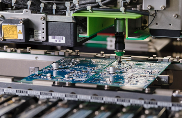
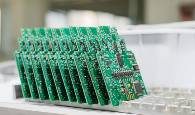
Wave soldering remains one of the most stable and cost-effective PCB assembly methods for through-hole components. Wave soldering is still widely used in industrial, power, automotive, and control electronics.
This guide explains wave soldering clearly, step by step, from a manufacturing engineer’s point of view.
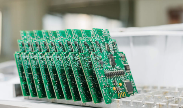
If you are looking for a reliable wave soldering manufacturer, EBest is a proven one-stop PCBA partner trusted by engineers worldwide.
What Is Wave Soldering in PCB Assembly?
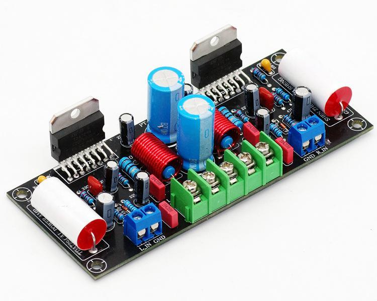
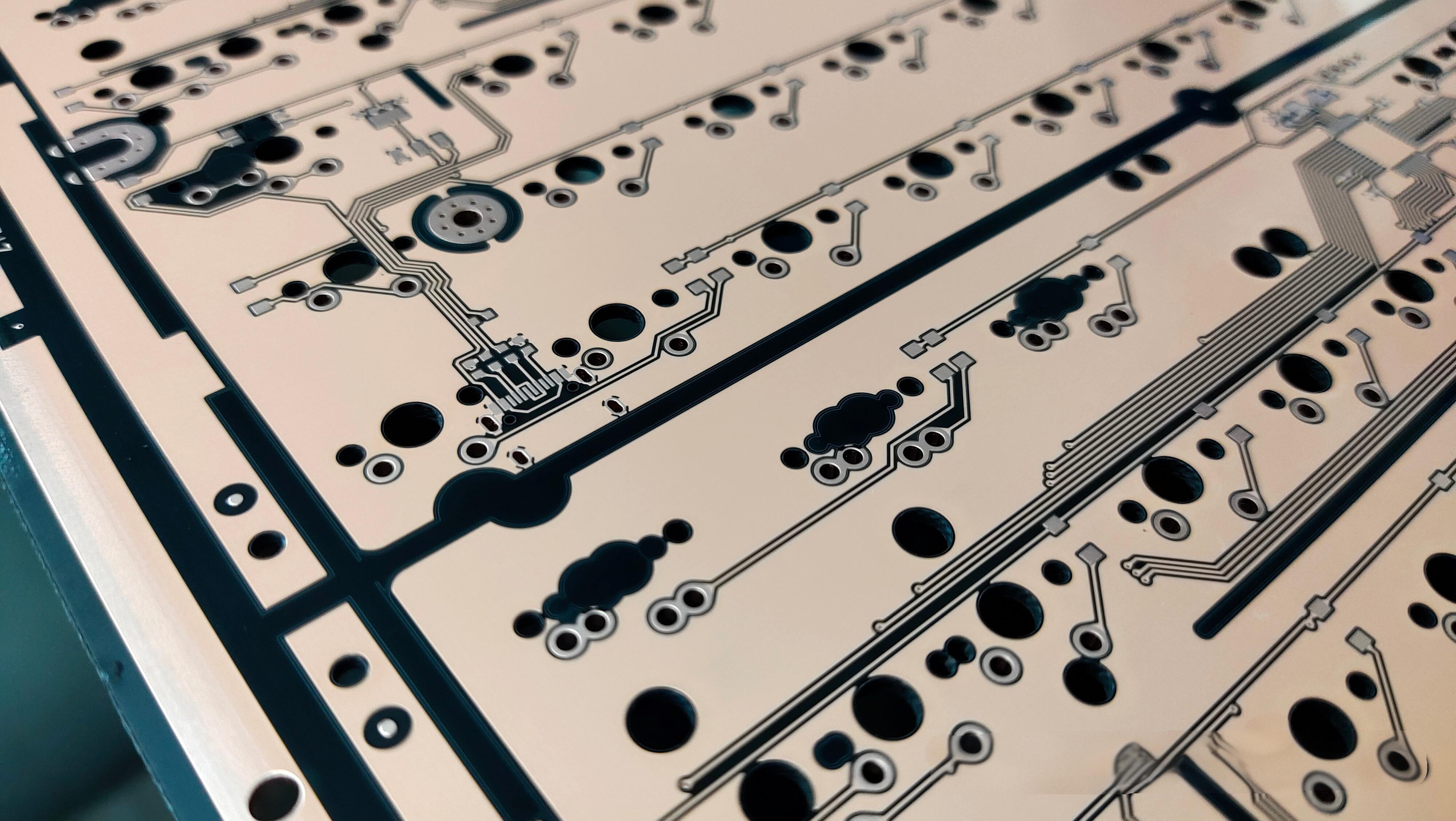
Wave soldering is a mass soldering process mainly used for through-hole PCB assembly.
In this process, the assembled PCB passes over a controlled wave of molten solder, forming solder joints simultaneously on all exposed pads and leads.
Why Is Wave Soldering Still Used Today?
Wave soldering is not “old tech.” It stays popular because it produces strong joints at high speed.
- Strong mechanical joints for connectors and large leads
- Stable quality due to controlled parameters
- Efficient throughput for medium to high volume production
Where Does Wave Soldering Fit Best?
Wave soldering is a strong match for designs that depend on physical strength and current capacity.
- Power supply boards and energy modules
- Industrial control boards and I/O boards
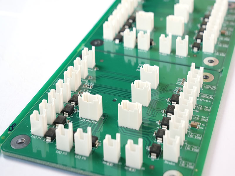
- Automotive and transportation modules with connectors
- Relay boards and mixed-technology assemblies

What Is Wave Soldering in PCB Assembly?
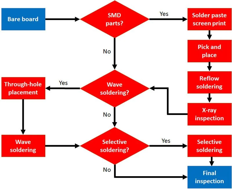
How Does the Wave Soldering Process Work Step by Step?
Wave soldering follows a strict sequence to control wetting, hole fill, and joint stability.
If one step drifts, defects show up quickly, so it helps to understand the logic behind each stage.
Step 1: Flux Application
Flux removes oxides and improves solder wetting on pads and component leads.
A good flux process is even, repeatable, and matched to your cleaning plan.
Common Flux Options
- No-clean flux (lower residue, less cleaning)
- Water-soluble flux (strong activity, typically needs cleaning)
- Rosin-based flux (traditional option, depends on chemistry)
What to Watch During Fluxing
- Coverage consistency across the full board width
- Flux density control and measurement discipline
- Overspray risk on keep-out areas
Step 2: Preheating
Preheating raises the PCB temperature gradually before solder contact.
This activates flux and reduces thermal shock, especially on thicker boards or heavy copper designs.
Why Preheat Matters
- Improves wetting and hole fill
- Reduces solder “skipping”
- Limits warpage and stress on parts
Step 3: Solder Wave Contact
The PCB passes over a molten solder wave at a controlled angle, speed, and contact time.
This is where joints form, so stability here drives yield more than any other stage.
Key Wave Contact Variables
- Solder pot temperature
- Wave height and wave stability
- Conveyor speed and contact time
- Board angle and component orientation
Step 4: Cooling
Cooling solidifies solder joints and impacts microstructure, appearance, and long-term reliability.
Controlled cooling reduces stress and can help avoid brittle joints on certain alloys.
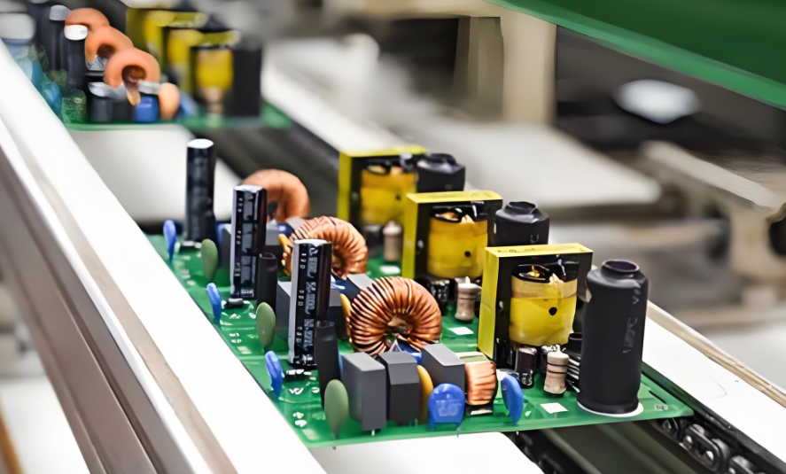
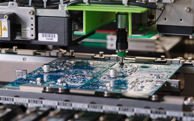
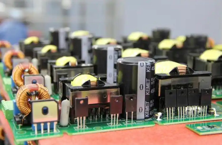
Here is a completed soldering process:
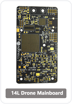
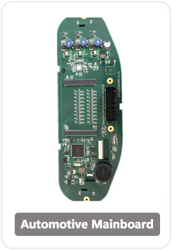
What Types of PCBs Are Best Suited for Wave Soldering?
Wave soldering is best when through-hole components dominate or when you need strong joints for connectors.
It is also common for mixed-technology boards where SMT is done first, then THT soldering is done by wave.
Typical Boards for Wave Soldering
- Connector-heavy boards (terminal blocks, headers, power connectors)
- High-current boards (power conversion, motor drives)
- Industrial control boards (I/O, relays, sensors)
- Transformer and coil assemblies
Can Mixed SMT and THT Boards Use Wave Soldering?
Yes. Mixed-technology boards can use wave soldering when SMT parts are protected.
Common protection methods include pallets, selective masking, adhesives for bottom-side parts, and orientation control.
What Are the Key Parameters in Wave Soldering?
Wave soldering success depends on controlling a small set of parameters with discipline.
The most important point is consistency: stable settings beat frequent adjustments.
Critical Wave Soldering Parameters
- Solder pot temperature (commonly around 245–265 °C depending on alloy and design)
- Conveyor speed (defines contact time)
- Flux density (affects activity and residue)
- Preheat temperature (affects wetting and thermal stress)
- Wave height and wave shape (affects bridging and hole fill)
How to Think About Parameter Tuning
Start with board constraints: thickness, copper weight, component thermal mass, and hole geometry.
Then tune preheat for stable activation, and only after that adjust wave contact and speed.
What Is the Difference Between Wave Soldering and Reflow Soldering?
Wave soldering and reflow soldering solve different assembly problems.
Reflow is dominant for SMT. Wave remains efficient for through-hole and connector-heavy designs.
| Comparison Item | Wave Soldering | Reflow Soldering |
|---|---|---|
| Primary Use | Through-hole, mixed-technology boards | SMT assembly |
| Solder Method | Molten solder wave | Solder paste + reflow profile |
| Mechanical Strength | High, strong joints on large leads | Good for SMT, less mechanical anchoring |
| Production Speed | High for suitable designs | High, but depends on paste printing and profile |
| Best Fit | Connectors, power parts, relays | Fine pitch ICs, high-density SMT |
When Should You Choose Wave Soldering Instead of Selective Soldering?
Choose wave soldering when the design is wave-friendly and throughput matters.
Choose selective soldering when you need localized soldering with less risk to nearby SMT parts.
Wave Soldering Is Often Better When
- Through-hole content is high
- Board layout is simple and spacing is safe
- Volume is medium to high
- Cost per board must be minimized
Selective Soldering Is Often Better When
- Dense mixed-technology boards need localized heating
- Bottom-side SMT parts are sensitive
- Only a few through-hole joints need soldering
What Are the Advantages of Wave Soldering?
Wave soldering delivers strong, repeatable joints at scale, especially on through-hole assemblies.
For many industrial boards, it remains the simplest path to stable quality.
Practical Advantages Engineers Notice
- High throughput for suitable designs
- Consistent solder joint formation when parameters are stable
- Excellent hole fill on properly designed through-holes
- Lower labor dependence than manual soldering
- Strong mechanical anchoring for connectors and heavy parts
What Are the Limitations of Wave Soldering?
Wave soldering is powerful, but it is not universal.
Understanding limits early helps you avoid layout choices that fight the process.
Typical Limitations
- Not suitable for fine-pitch SMT on the wave side without protection
- Higher risk of bridging if spacing is tight
- More design constraints than reflow for mixed layouts
What Are Common Wave Soldering Defects and Their Causes?
Most wave soldering defects are predictable. That is good news.
Once you link defect patterns to root causes, yield improvement becomes systematic.
| Defect | Typical Root Cause | Common Fix |
|---|---|---|
| Solder Bridging | Excess solder, poor spacing, high wave height | Reduce wave height, improve pad spacing, adjust angle |
| Icicles / Solder Spikes | Low solder temperature or poor peel-off | Increase pot temperature, adjust speed and angle |
| Solder Skips | Oxidation, insufficient flux, poor preheat | Improve fluxing, tune preheat, check surface finish |
| Cold Joints | Insufficient heat input or contamination | Increase preheat, stabilize pot temperature, improve cleaning |
| Blow Holes / Voids | Moisture in PCB or components | Bake boards, improve storage and handling |
How Can You Reduce Wave Soldering Defects?
Defect reduction works best when you combine DFM discipline with stable process control.
Think in two layers: what you fix in design, and what you lock down in production.
Design-Level Practices That Help
- Maintain safe pad spacing to reduce bridging risk
- Use proper annular ring size for hole fill stability
- Control lead protrusion length to reduce icicles
- Plan component orientation to support clean peel-off
Process-Level Practices That Help
- Measure flux density consistently, not occasionally
- Keep preheat profiles stable across shifts
- Maintain solder pot cleanliness and dross control
- Use inspection feedback (AOI, visual, X-ray when needed)
How Much Does Wave Soldering Cost in PCB Assembly?
Wave soldering cost depends on design complexity and volume, but it usually becomes more economical as volume rises.
Boards with many through-hole connectors often benefit most because wave soldering replaces time-consuming hand soldering.
What Drives Cost in Real Projects?
- Board size and thickness
- Through-hole count and pitch density
- Flux and solder alloy choice
- Masking or pallet requirements for mixed boards
- Inspection and reliability requirements
Why Choose EBest as Your Wave Soldering Manufacturer?
If you need stable wave soldering results, you need more than a machine. You need engineering control.
EBest is a one-stop PCBA service provider, built to better understand the needs of engineers.
What You Get with EBest
- Free DFM and process adaptation suggestions
- 20 years of experience serving 1,800+ customers and 10,000+ engineers
- One-Stop Service: PCB, components, PCBA, testing, and box-building
- No MOQ and personal service for prototypes
- Certifications: ISO9001, ISO13485, IATF16949, AS9100D
- MES and full traceability
- 1.5-week rapid PCBA delivery
- Technical support before and after sales
- Quick turn-out with on-time delivery focus
- Prompt feedback within 12 hours
FAQ — Common Questions About Wave Soldering
What is wave soldering mainly used for?
Wave soldering is mainly used for through-hole components, especially connectors and parts that need strong mechanical joints.
Is wave soldering still relevant today?
Yes. Wave soldering is still common in industrial control, power electronics, and connector-heavy designs.
Can wave soldering handle mixed-technology boards?
Yes, but you need proper masking, orientation planning, and protection for sensitive SMT parts on the wave side.
Does EBest welcome prototypes or small-quantity orders?
Yes. EBest supports prototypes and small volume runs with personal engineering support.
Do you offer quick-turn production for wave soldering PCBA?
Yes. EBest supports quick-turn schedules, including 1.5-week rapid PCBA delivery for eligible builds.
What files do you need to quote wave soldering PCB assembly?
Typically you need Gerbers, BOM, pick-and-place (if SMT is included), assembly drawings, and special process notes.
Final Call to Action
If you need wave soldering or complete PCBA services, EBest is ready to support your project.
We deliver reliable wave soldering solutions with fast turnaround, disciplined quality control, and full traceability.
Contact us to place your order: sales@bestpcbs.com
EBest — One-stop PCBA service provider, better understanding the needs of engineers.