Copper thermal conductivity plays a significant role in its widespread use across various industries. When it comes to heat transfer, copper is often seen as the go-to material due to its exceptional ability to conduct heat. In this blog, we will explore how copper compares to other metals, especially aluminum, and how its thermal properties impact its performance in different environments. Let’s dive into the world of heat conductivity, from copper’s efficiency to its temperature-dependent behavior.
What Is the Thermal Conductivity of Copper?
Thermal conductivity refers to a material’s ability to conduct heat. Copper stands out as one of the best conductors of heat, making it a popular choice in industries where efficient heat transfer is crucial. The thermal conductivity of copper is approximately 398 W/m·K at room temperature. This high value makes copper the preferred material for various applications, from electrical wiring to heat exchangers.
Interestingly, pure copper offers even higher thermal conductivity compared to alloys, making it an essential material in applications requiring optimal heat management.
What Is the Best Conductor of Heat?
While many metals offer good thermal conductivity, copper is often regarded as the best conductor of heat. Silver, in fact, has a slightly higher thermal conductivity than copper, but due to its cost and scarcity, silver is rarely used in practical applications. Copper’s balance of affordability and efficiency makes it the top choice for industries where heat transfer is critical, such as electronics, automotive, and HVAC systems.
Aluminum, although a good conductor, falls behind copper in terms of efficiency. Copper’s superior performance in both heat conductivity and durability makes it a more reliable material in most heat management scenarios.
What Is the Thermal Conductivity of Copper vs Aluminum?
When comparing the thermal conductivity of copper vs aluminum, copper wins hands down. Aluminum has a thermal conductivity of around 235 W/m·K, which is significantly lower than copper’s. This difference may seem small, but it has a big impact in fields such as electronics and engineering, where heat dissipation is critical.
Copper’s higher conductivity means that it can transfer heat more effectively, making it a better choice for applications that require rapid heat transfer. However, aluminum’s lighter weight and lower cost make it a viable alternative in situations where heat conductivity is not the top priority.
How Does Copper Compare to Other Metals in Thermal Conductivity?
Copper is often compared to metals like aluminum, brass, and nickel. While aluminum is a good conductor, copper far surpasses it in efficiency. On the other hand, brass, which is an alloy of copper and zinc, has lower thermal conductivity than pure copper. Similarly, nickel’s thermal conductivity is also lower than copper’s, which makes copper a preferred material when high heat transfer is needed.
For instance, silver may have the highest thermal conductivity of all metals, but its cost makes it impractical for most applications. Copper strikes a perfect balance, offering excellent heat transfer without the high price tag associated with silver.
How Does Temperature Affect Copper’s Thermal Conductivity?
Copper’s thermal conductivity does not remain constant as temperatures change. As the temperature increases, copper’s thermal conductivity decreases. This is because the atomic vibrations in copper increase with temperature, disrupting the smooth flow of heat.
At room temperature, copper’s conductivity is at its peak. However, as the temperature rises, its ability to conduct heat diminishes. This temperature-dependent behavior must be considered in high-heat applications such as electronics and manufacturing, where managing temperature fluctuations is critical.
At What Temperature Does Copper Melt?
Copper melts at a temperature of 1,984°F (1,085°C). This relatively high melting point is another reason copper is highly favored in industries dealing with extreme temperatures, such as aerospace and power generation. Unlike materials with lower melting points, copper maintains its integrity under heat, providing reliability and durability.
Is Copper or Aluminum Better for Cooling?
When it comes to cooling efficiency, copper generally outperforms aluminum due to its superior thermal conductivity. However, aluminum is often used in cooling applications where weight is a crucial factor, such as in the automotive industry. Copper’s heavier weight might make it less suitable for such purposes, but in situations where heat needs to be transferred quickly and efficiently, copper is the better choice.
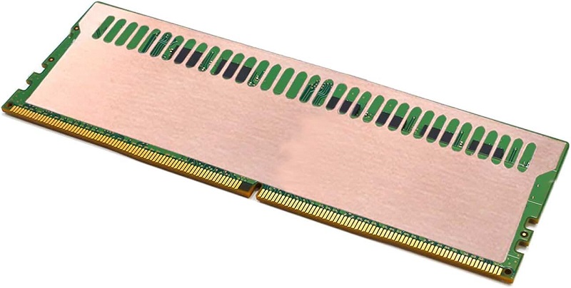
In cases like computer processors, where efficient cooling is paramount, copper is often used for heat sinks because of its superior ability to absorb and dissipate heat.
Why Does Copper Have a High Thermal Conductivity?
Copper’s high thermal conductivity can be attributed to its atomic structure. The metal has a highly ordered arrangement of atoms, which allows heat to flow more easily through the material. Additionally, copper’s free electrons move quickly, aiding in the rapid transfer of heat. This ability to efficiently conduct heat is one of the reasons copper is so widely used in heat exchangers, electrical wiring, and other applications where heat dissipation is essential.
In summary, the thermal conductivity of copper makes it the material of choice for a variety of high-performance applications. Whether you’re considering copper vs aluminum thermal conductivity for your projects or exploring how copper compares to other metals like brass or nickel, copper consistently outperforms its competitors in heat transfer efficiency. While aluminum may be lighter and more cost-effective in some situations, copper’s superior thermal properties make it the go-to material in industries where heat management is critical.
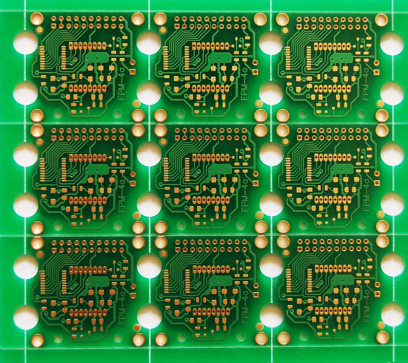
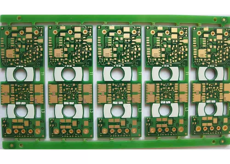
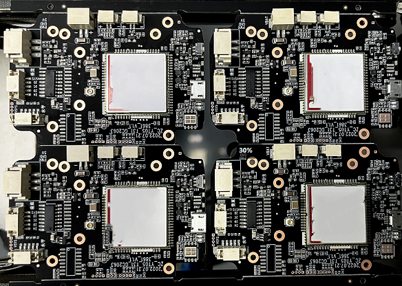
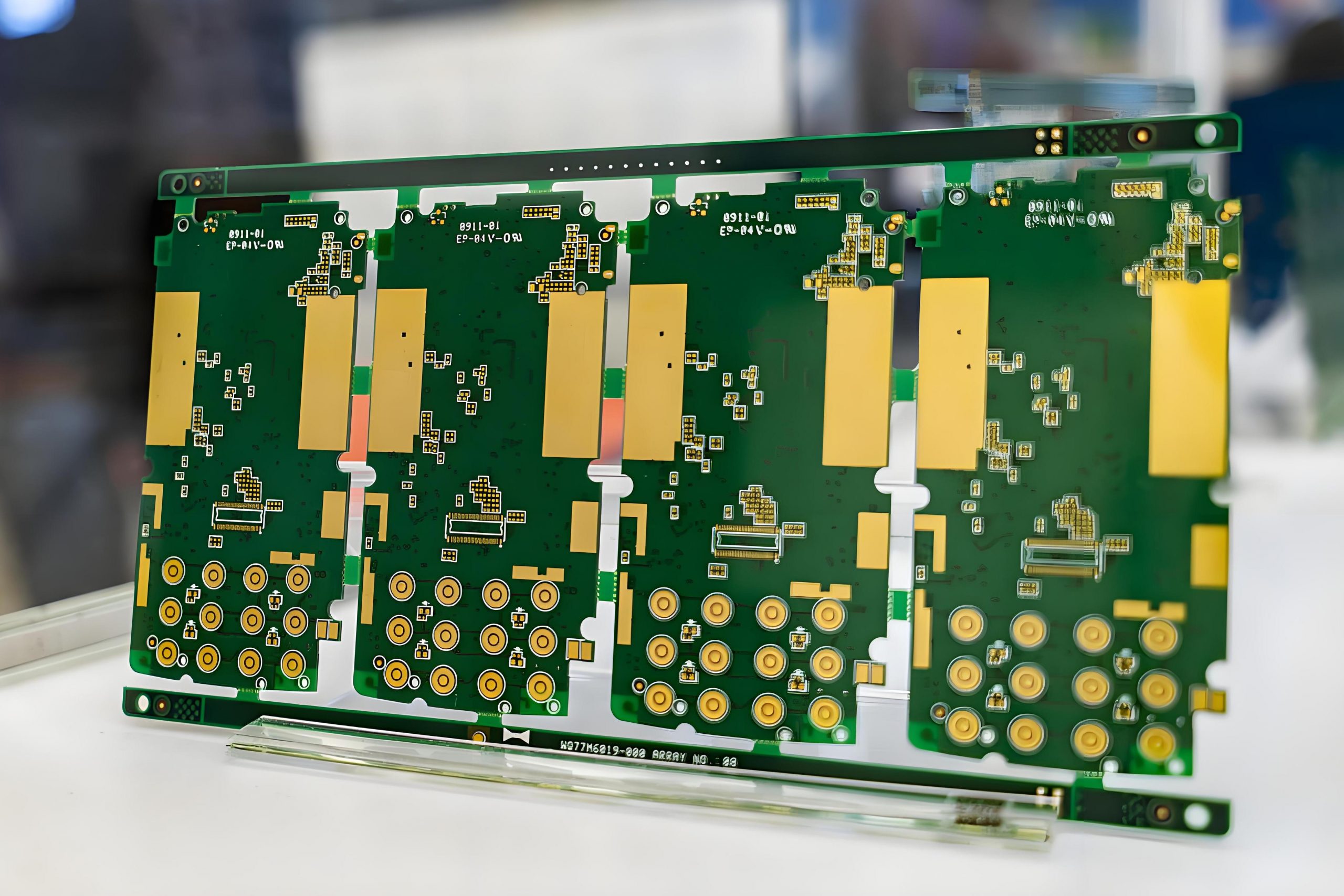
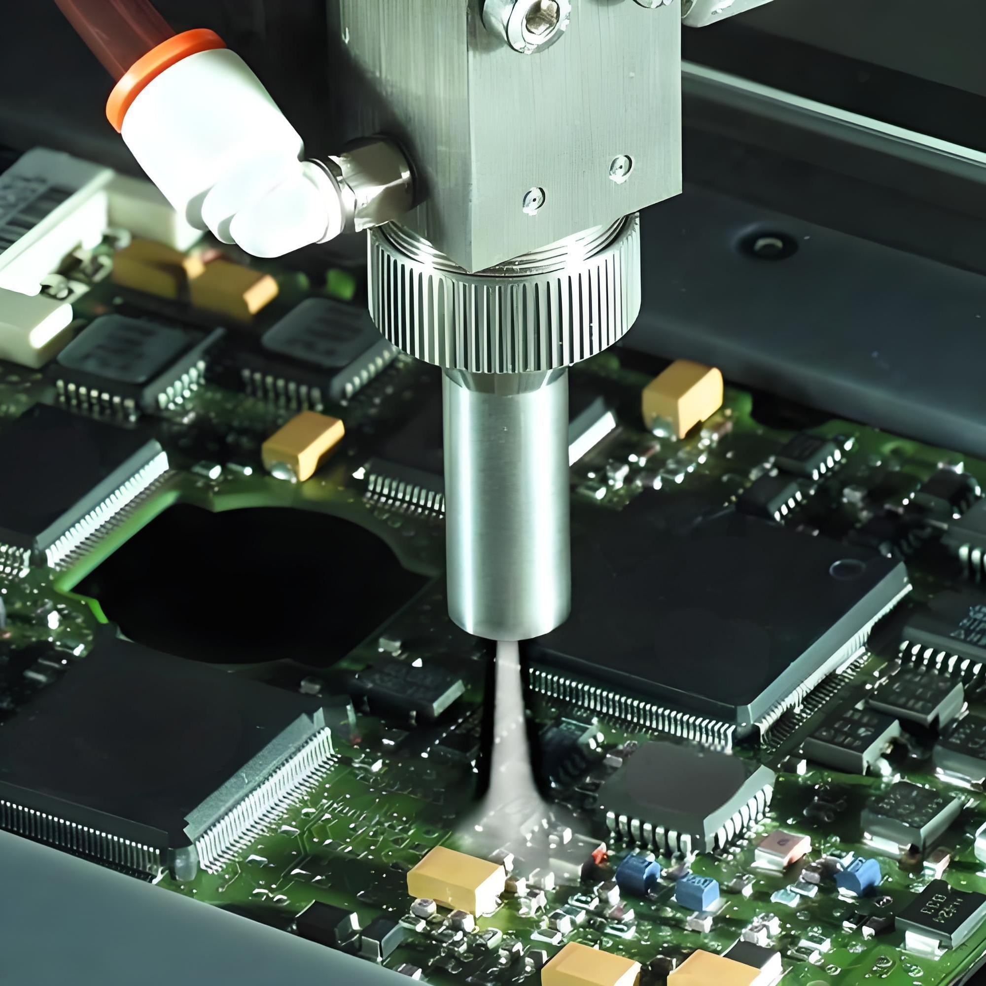
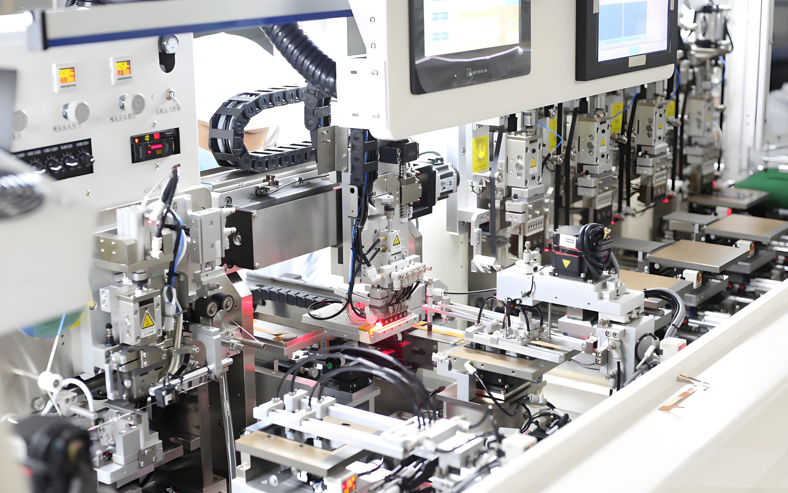
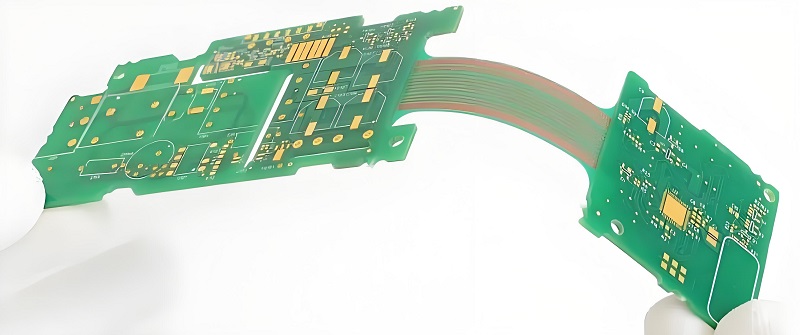
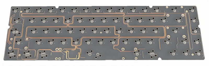
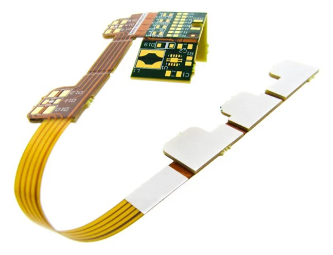
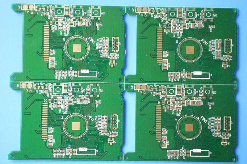
At EBest Circuit (Best Technology), we specialize in high-quality PCBs designed for optimal thermal performance. With over 18 years of experience in the industry, we provide solutions tailored to your specific needs. If you’re looking for a reliable partner in heat management, reach out to us at sales@bestpcbs.com for more information or questions.