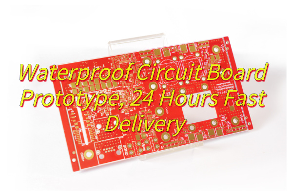
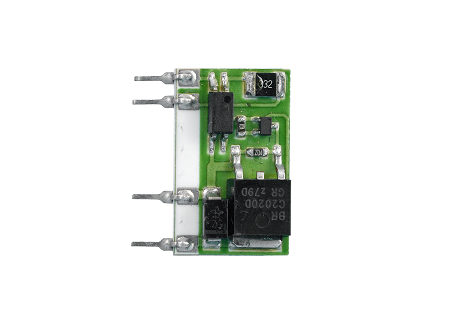
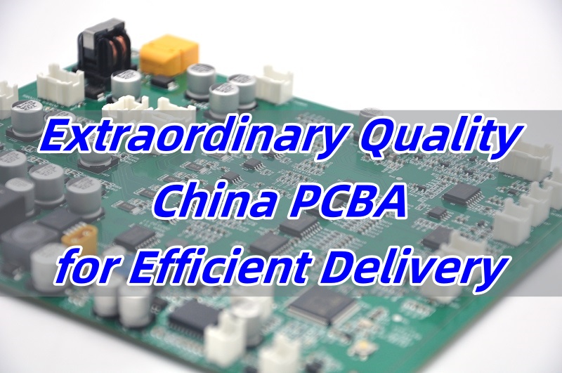
China SMT PCBA is the first choice for many global brands when they need speed, flexibility, and quality all in one package. In recent years, more companies have switched to turnkey services to cut costs and reduce lead time. But not all suppliers are equal. That’s why understanding what makes a solution truly premium is key to making the right decision.
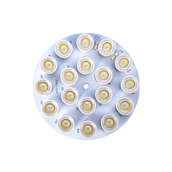
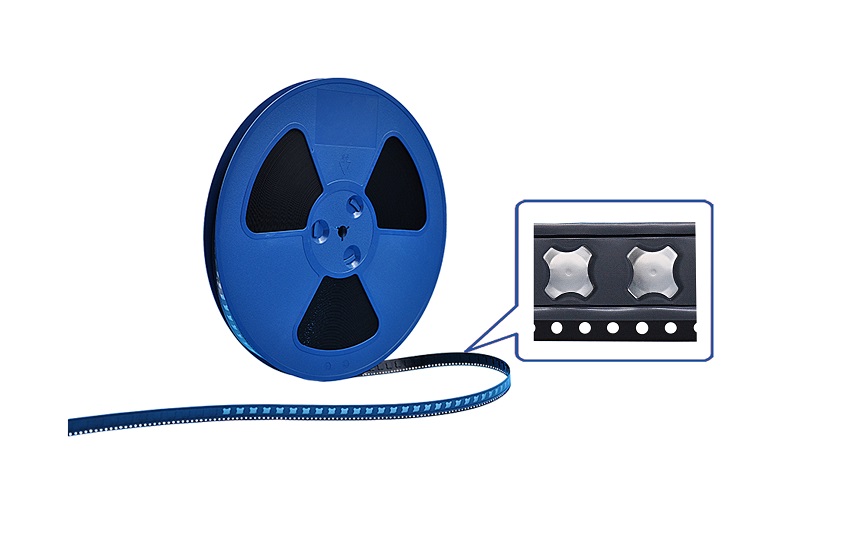
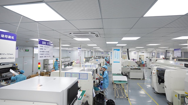
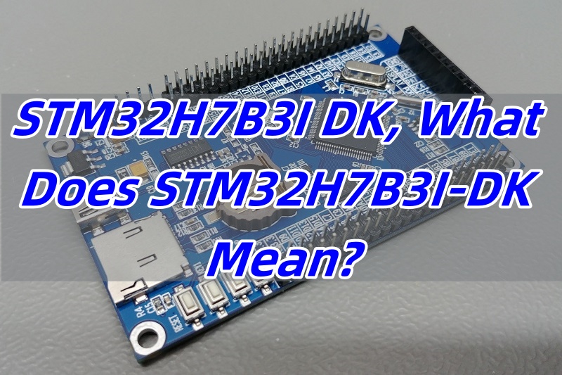
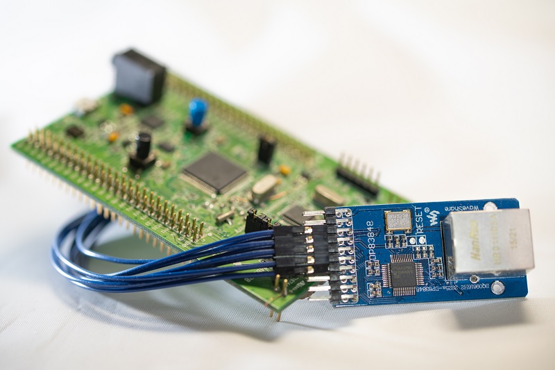
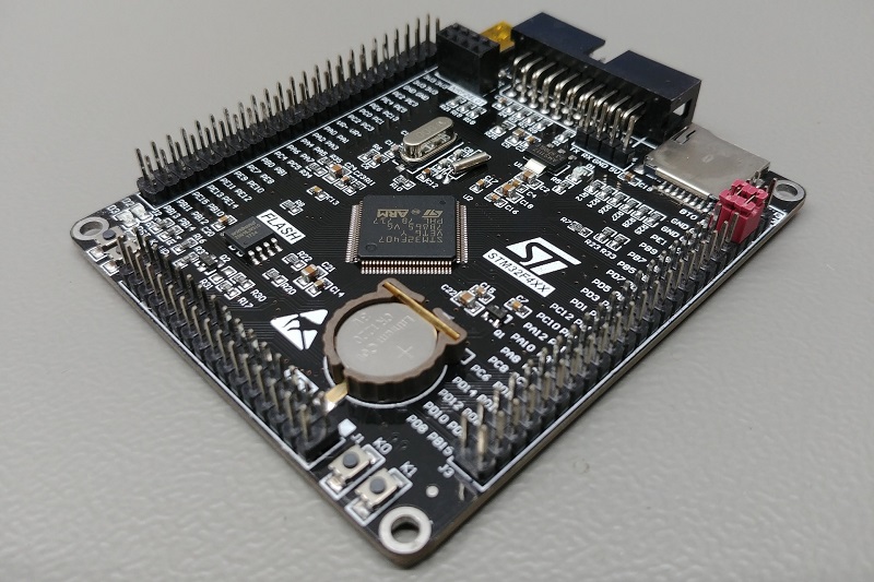
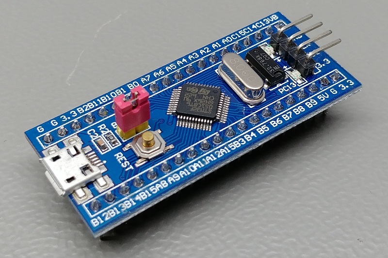
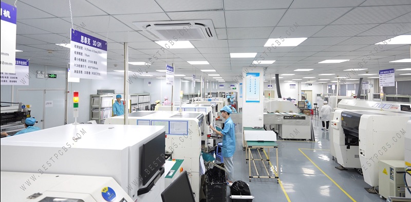
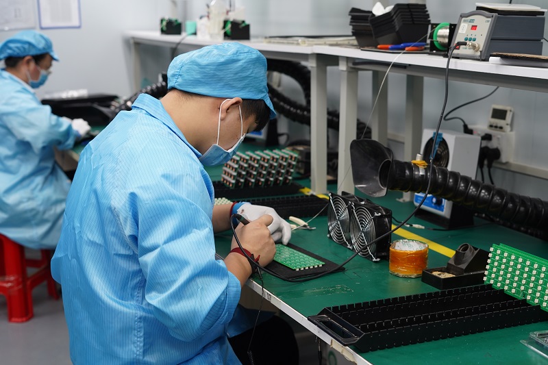
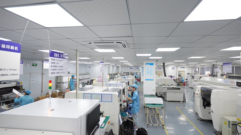
EBest Circuit (Best Technology) offers premium quality China SMT PCBA turnkey solutions in the global market. Our customer orders can be routed flexibly through our SMT facilities in China or Vietnam, subject to technical requirements and trade considerations. The advanced equipment, comprehensive process control, and intelligent manufacturing capabilities give us a competitive edge over the average competitors. Our SMT factories are equipped with state-of-the-art equipment, including high-speed chip mounters from Panasonic, as well as SMT PCBA machines from YAMAHA and JUKI. We also utilize advanced inspection tools, such as 3D AOI, X-ray machines, and 3D SPI. Feel free to send us an e-mail at sales@bestpcbs.com for turnkey SMT PCBA solutions.
What Services Are Included in a China SMT PCBA Turnkey Solution?
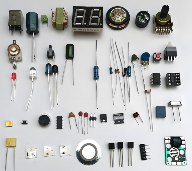
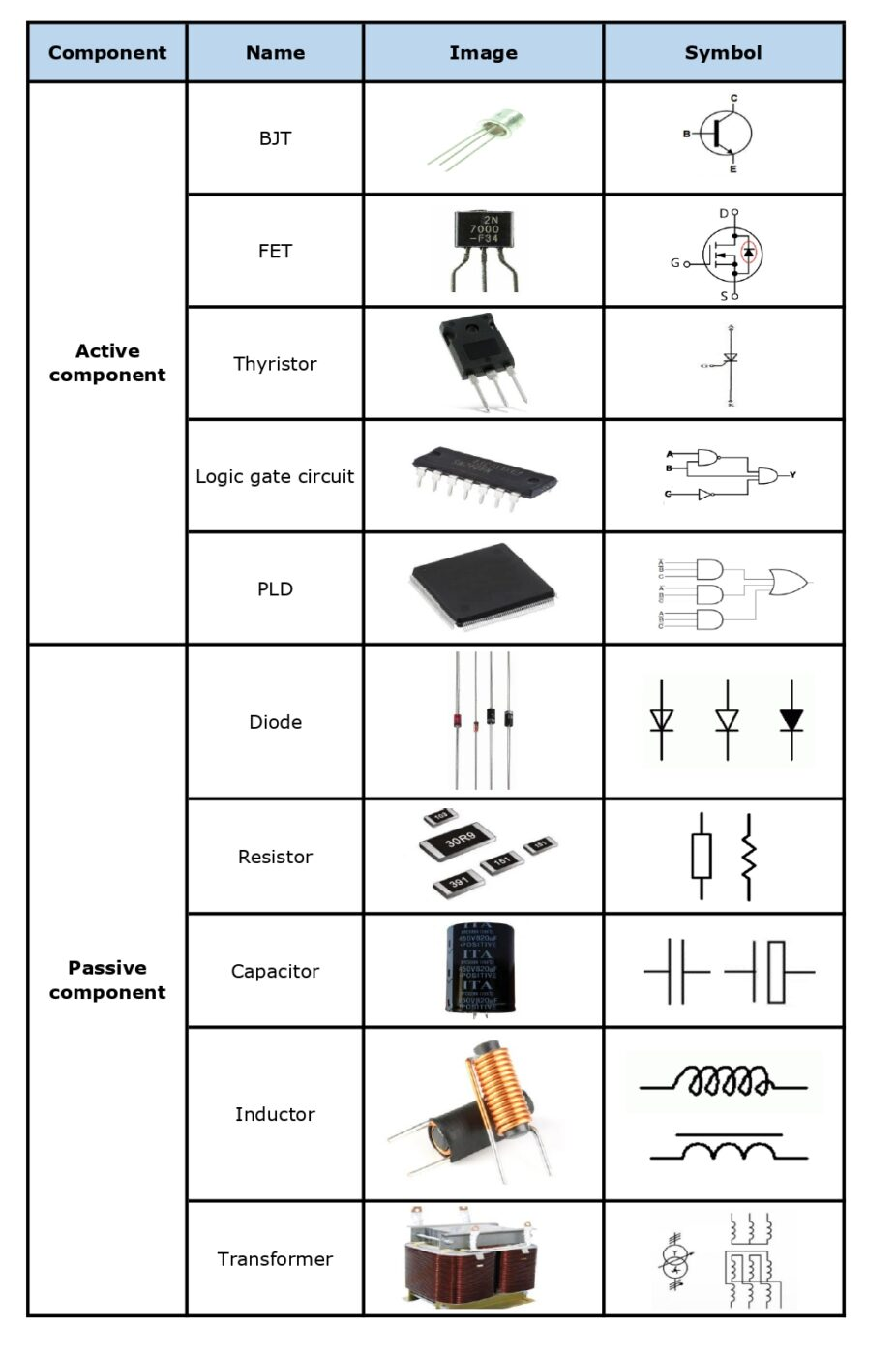
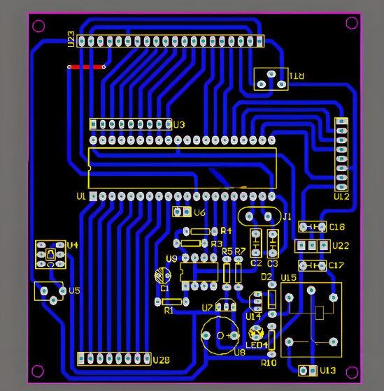
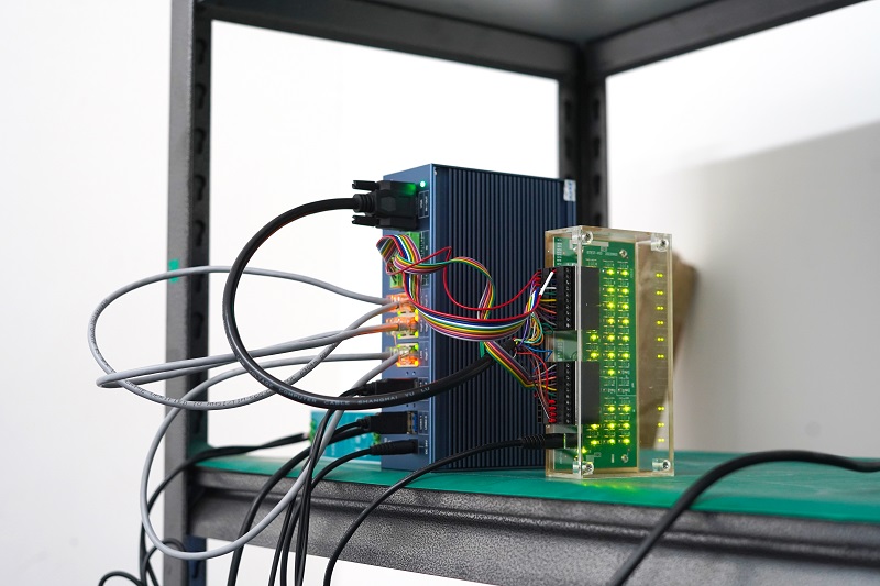
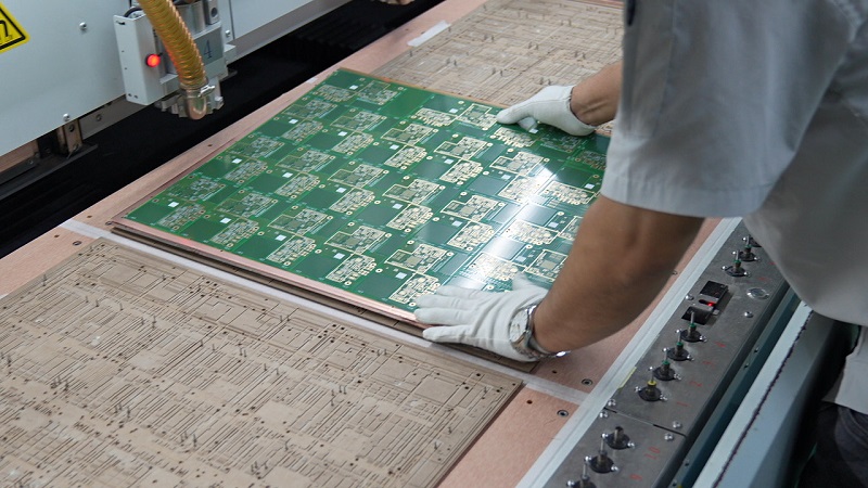
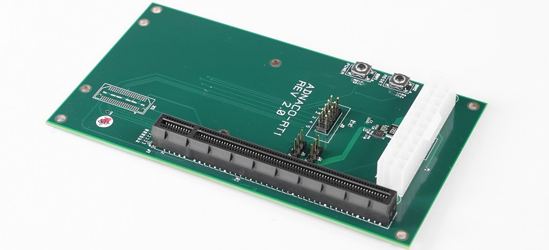
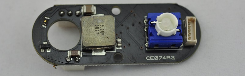
A full turnkey service means more than just soldering components. It covers the entire journey—component sourcing, PCB fabrication, SMT and DIP assembly, testing, packaging, and even delivery. Some providers also assist with design verification or offer DFM checks early in the process to prevent future issues. With a reliable partner, you get all services from a single source, reducing delays and miscommunication.
Who Is the Best Manufacturer of China SMT PCBA?
The best partner is one who delivers quality consistently and solves customer demands. EBest Circuit (Best Technology) stands out for its combination of advanced MES systems, certified quality management (ISO 9001, ISO 13485, IATF 16949, AS9100D), and real-time material tracking. It’s not just about making boards. It’s about helping customers reduce their defect rate, stay on schedule, and get traceable production data.
Who Is the Largest China SMT PCBA Manufacturer?
While there are large players like Foxconn or BYD that serve big OEMs, mid-size companies often need faster responses and more flexibility. That’s where EBest Circuit (Best Technology) shines. With factories in both Shenzhen and Dongguan, and dedicated engineering teams, Best offers tailored PCBA services without the high MOQs and long queues seen at large OEM suppliers.
How Does PCBA in China Compare to Other Regions in Terms of Cost and Quality?
China provides a unique mix of cost advantage and technical depth. While countries like Vietnam offer lower wages, they often lack strong supply chains and technical support. In contrast, China SMT PCBA manufacturers like EBest Circuit (Best Technology) combine automation, quality control, and skilled labor, which drives down rework rates and total cost over the project lifecycle.
How to Evaluate the Quality of a China SMT PCBA Manufacturer?
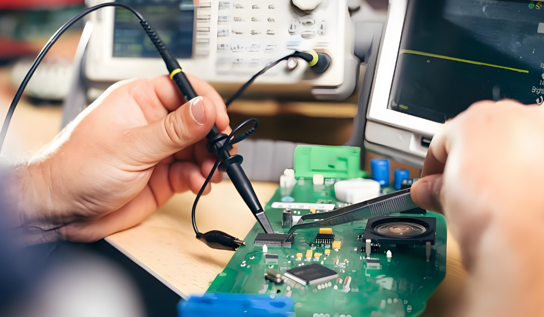
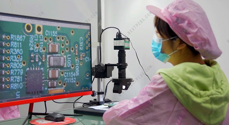
Start with certifications. Look for ISO, IATF, or medical-grade credentials. Then dig deeper. Do they use SPI, AOI, ICT, and X-ray inspection? Can they provide traceable data for every step? At EBest Circuit (Best Technology), full process control and material tracking are standard. Our MES system gives real-time visibility into material use, which helps solve problems like stock errors or replenishment delays.
What Should You Check Before Choosing a China SMT PCBA Manufacturer?
Check these points:
- Do they have in-house PCB fabrication or rely on outsourcing?
- Is their SMT line modern and well-maintained?
- Do they provide DFM or DFx reviews?
- Can they handle small batch orders and scale when needed?
- Do they support after-sales engineering and rework?
EBest Circuit (Best Technology) not only ticks all the above boxes but also helps manage unexpected changes. Whether it’s last-minute part replacements or urgent lead time adjustments, we respond fast with flexible production plans.
Why Choose EBest Circuit (Best Technology) for China SMT PCBA?
Here’s why so many brands rely on us:
- ERP + MES Integration: We solve warehouse and stock visibility issues by using ERP and MES systems. No more line-side material delays.
- Intelligent Production: Our SMT lines include inline SPI, AOI, and X-ray checks, reducing solder defects like cold joints, shorts, or bridging.
- Responsive Team: Fast DFM feedback, rapid quote turnaround, and 24/7 engineering support make project launch smoother.
- Custom-Tailored Support: We help you find the balance between cost and quality, even with complex or high-mix builds.
To sum up, choosing the right China SMT PCBA partner is more than finding the lowest price. It’s about trust, responsiveness, and being ready to handle complexity. EBest Circuit (Best Technology) doesn’t just assemble boards. We help solve deeper challenges—like poor stock management, unclear traceability, inconsistent soldering, and late deliveries.
With our strong process control, real-time systems, and highly responsive team, we help you reduce risk, speed up delivery, and improve product reliability. If you’re looking for a long-term PCBA partner who understands real manufacturing needs, we’re ready to help. Please feel free to e-mail us directly at sales@bestpcbs.com for a viable solution for China SMT PCBA.