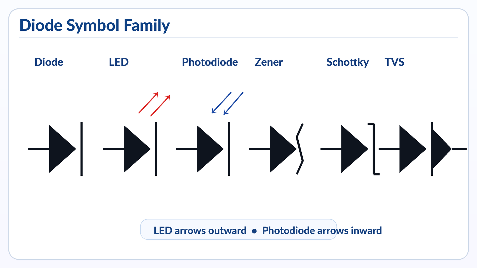
The LED symbol is the schematic symbol used to represent a light-emitting diode in an electrical circuit. It looks like a standard diode symbol with two small arrows pointing outward, showing that the component emits light when current flows in the correct direction.
What Does the LED Symbol Mean?
The LED symbol means a light-emitting diode, a polarized semiconductor component that allows current to flow mainly in one direction and produces light during operation. In a schematic, it is normally drawn as a diode shape with two arrows pointing away from it.
The diode part of the symbol shows electrical direction. The outward arrows show light emission. This is the easiest way to distinguish an LED from a normal rectifier diode. When reading a circuit diagram, the symbol tells you three things at once: the component type, its polarity, and the intended current direction.
A basic LED symbol includes these parts:
| Symbol Part | Meaning | Practical Design Note |
| Diode body | Current flows in one direction | LED must be placed with correct polarity |
| Vertical bar | Cathode side | Often linked to the shorter lead or marked side |
| Opposite side | Anode side | Usually connects toward positive supply through a resistor |
| Two outward arrows | Light emission | Confirms it is an LED, not a normal diode |
| Reference designator | Usually D, LED, or DS | Must match BOM and PCB silkscreen |
Why Is the LED Symbol Important in Circuit Diagrams and PCBs?
The LED symbol is important because LEDs are polarized components. A resistor, capacitor, or connector may still be visually clear after placement, but an LED can easily be mounted in the wrong direction if the symbol and PCB marking are unclear.
In a schematic, the LED symbol helps engineers understand circuit logic. In a PCB layout, it helps the manufacturer place the part correctly. In assembly inspection, it gives the operator and AOI system a visual reference for orientation.
A wrong LED symbol may look like a small drafting issue, but in production it can become a batch-level assembly defect. For LED PCBA projects, the schematic symbol, PCB footprint, silkscreen polarity mark, and BOM package must be checked together before manufacturing.
How Does an LED Work in a Circuit?
An LED works by converting electrical energy into light when forward current passes through its semiconductor junction. The anode connects to the more positive side of the circuit, and the cathode connects toward the lower potential side.
In most simple circuits, current flows from the power source, through a resistor, into the LED anode, out from the cathode, and back to ground. The resistor is important because an LED does not naturally limit current like a lamp filament. Without proper current control, excessive current can overheat the LED, reduce brightness stability, or damage the component.
A basic LED circuit usually look like:
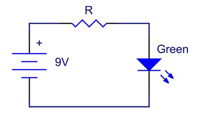
For a single indicator LED, the electrical load is small. For high-power LED boards, lighting panels, or dense LED arrays, current, heat, copper thickness, substrate material, and solder joint reliability become much more important.
How Do You Identify the Anode, Cathode, and Current Direction?
The anode is the positive side of an LED, and the cathode is the negative side. In the schematic symbol, the cathode is normally shown by the vertical bar. Current flows from anode to cathode under forward bias.
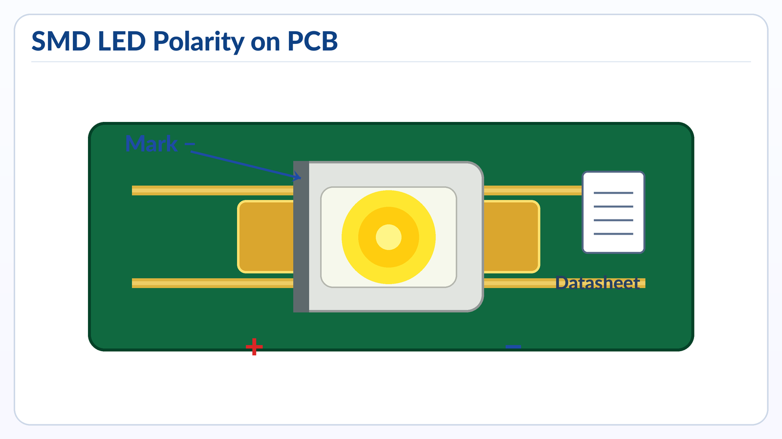
For through-hole LEDs, the longer lead is usually the anode, while the shorter lead is usually the cathode. Many round LEDs also have a flat edge on the cathode side. For SMD LEDs, polarity marks vary by package and manufacturer. Some use a green mark, chamfered corner, printed line, notch, or datasheet-defined pad shape.
Because SMD polarity markings are not universal, engineers should not rely only on memory. The safest method is to compare three items:
| Item to Check | What to Confirm |
| LED datasheet | Pin 1, anode, cathode, package drawing |
| Schematic symbol | Correct anode/cathode orientation |
| PCB footprint | Pad numbering and polarity mark |
| Silkscreen | Clear A/K or diode mark |
| Pick-and-place file | Rotation angle matches assembly standard |
What Are the Main Types of LED Symbols and Related Diode Symbols?
The standard LED symbol is a diode symbol with two arrows pointing outward. However, engineers often compare it with other diode-related symbols during schematic reading.
| Symbol Type | Visual Difference | Meaning | Common Use |
| Standard diode | Diode shape only | One-way current flow | Rectification, protection |
| LED | Diode with outward arrows | Emits light | Indicators, lighting, displays |
| Photodiode | Diode with inward arrows | Responds to light | Sensors, optical receivers |
| Zener diode | Diode with bent cathode line | Voltage regulation | Clamping, reference circuits |
| Schottky diode | Modified diode symbol | Low forward voltage | Fast switching, power circuits |
| Laser diode | LED-like symbol with optical indication | Coherent light emission | Optical modules, laser systems |
Which LED Packages and Materials Affect PCB Design?
LED package type affects PCB footprint design, soldering process, thermal management, optical alignment, and assembly inspection. A small indicator LED has very different PCB requirements from a high-power LED used in automotive lighting or industrial illumination.
Common LED package types include:
| LED Type | Typical Use | PCB Design Focus | Relative Cost |
| Through-hole LED | Basic indicators, panels | Hole size, polarity, lead forming | Low |
| 0603/0805/1206 SMD LED | Compact indicators | Footprint accuracy, AOI visibility | Low to medium |
| PLCC LED | Backlight, signage, automotive interiors | Heat spreading, optical direction | Medium |
| COB LED | High-density lighting | Thermal path, substrate flatness | Medium to high |
| High-power LED | Lighting, automotive, industrial | MCPCB or ceramic substrate, heat control | High |
| RGB LED | Displays, decorative lighting, status signals | Pin mapping, color channel routing | Medium |
| Addressable LED | Smart lighting, LED strips | Data signal routing, power integrity | Medium to high |
LED semiconductor material also affects color, forward voltage, luminous efficiency, and heat behavior. For example, red and amber LEDs often have lower forward voltage than blue or white LEDs. White LEDs usually use blue LED chips with phosphor conversion, so optical quality and heat aging are important.
What Are the Benefits and Limits of Using LEDs in Electronic Products?
LEDs are popular because they are compact, efficient, fast-switching, and easy to integrate into PCB assemblies. They can provide simple status indication or support complex lighting, sensing, display, and communication functions.
Main benefits include:
- Low power use compared with many older light sources
- Long service life under proper current and thermal conditions
- Small package options for compact PCBs
- Fast response for signal indication and optical communication
- Wide color selection
- Easy integration with microcontrollers
- Suitable for automated SMT assembly
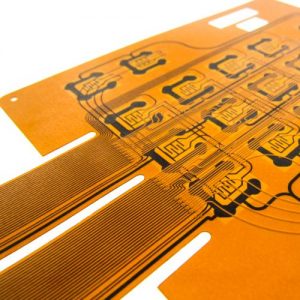
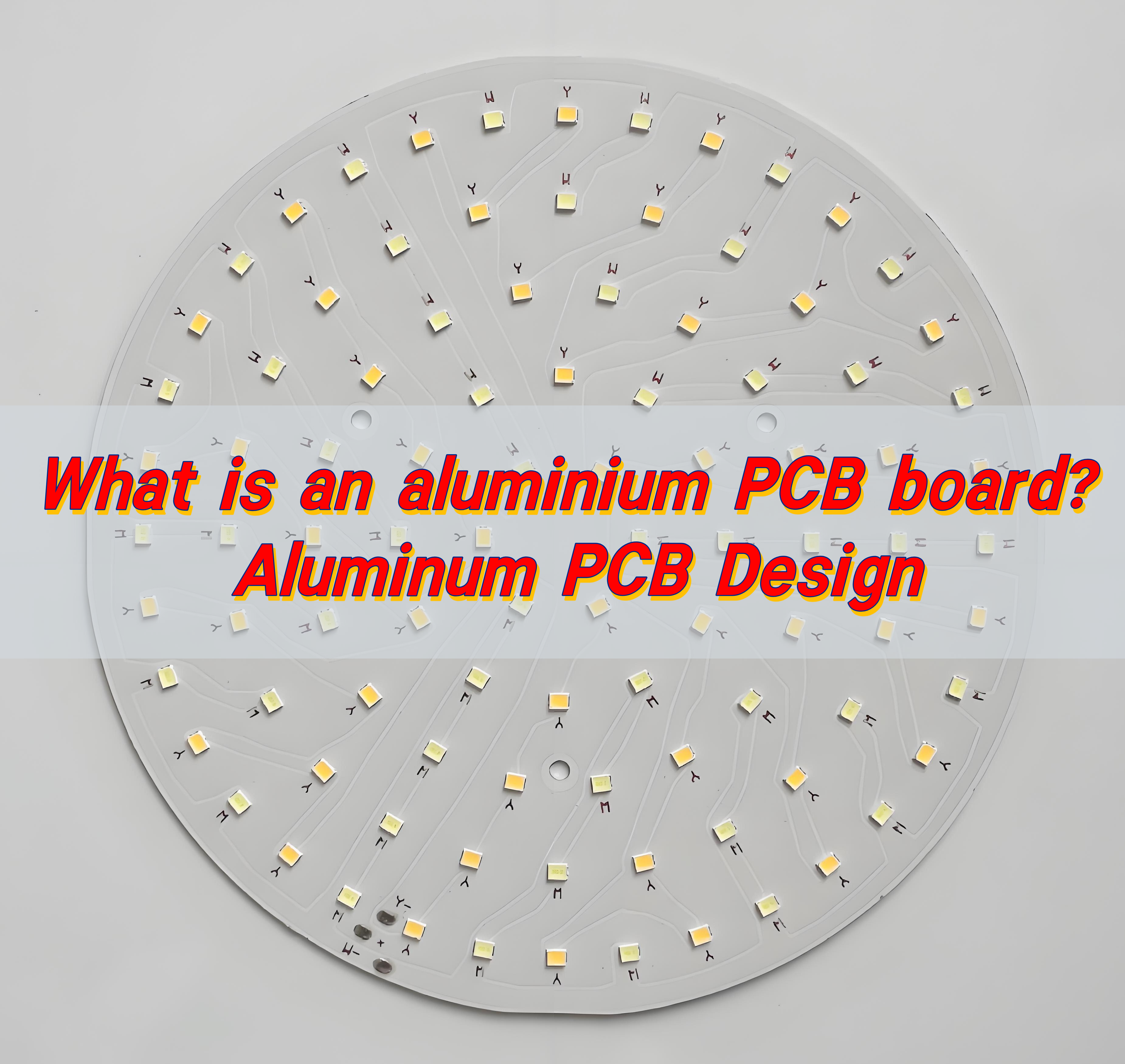
LEDs also have practical limits. Their brightness changes with current, temperature, viewing angle, lens structure, and binning. High-power LEDs need careful heat dissipation. RGB or addressable LEDs need correct pin mapping and signal integrity. Dense LED arrays may require heavier copper, thermal vias, aluminum PCB, copper substrate, or ceramic PCB depending on power density.
LED Symbol vs Diode Symbol vs Photodiode Symbol: What Is the Difference?
The LED symbol, diode symbol, and photodiode symbol all come from the diode family, but they show different functions. A normal diode controls current direction. An LED emits light. A photodiode detects light.
| Feature | Diode Symbol | LED Symbol | Photodiode Symbol |
| Main function | Allows one-way current flow | Emits light | Converts light into electrical signal |
| Arrow direction | No light arrows | Arrows point outward | Arrows point inward |
| Polarity | Anode and cathode | Anode and cathode | Anode and cathode |
| Typical circuit role | Rectifier or protection | Indicator or light source | Sensor or receiver |
| Common PCB risk | Wrong orientation | Wrong orientation or brightness issue | Wrong bias or sensitivity issue |
What Manufacturing and Quality Checks Matter for LED PCBA?
LED PCBA quality depends on correct component orientation, stable soldering, controlled heat, clean optical surfaces, and suitable electrical testing. A board can pass basic continuity checks but still fail brightness, color, or alignment requirements.
During manufacturing, important checks include:
- Incoming LED part number verification
- Polarity confirmation before SMT setup
- Solder paste inspection for fine SMD LEDs
- SMT placement angle and orientation check
- Reflow profile control
- AOI inspection for missing, shifted, or reversed LEDs
- Functional test for brightness and on/off logic
- Visual inspection for lens contamination
- Thermal check for high-power LED modules
- Sample aging or burn-in when required by application
For high-volume LED boards, a first article inspection is useful. The first assembled board should be checked against the schematic, PCB layout, BOM, polarity marks, and functional test procedure before full production begins.
For LED lighting boards, thermal design is especially important. FR4 may be enough for low-power indicators, but aluminum PCB, copper core PCB, or ceramic PCB may be more suitable when heat is concentrated near high-power LEDs.
What Common LED Failures Come from Symbol or Polarity Mistakes?
Many LED failures are not caused by bad components. They come from symbol mismatch, footprint errors, polarity confusion, poor current control, or weak thermal design.
| Failure Mode | Common Cause | Factory-Level Prevention |
| LED does not light | Reversed polarity or open circuit | Check symbol, footprint, and AOI direction |
| LED burns out | No resistor or excessive current | Verify current calculation and driver design |
| Uneven brightness | LED binning mismatch or resistor tolerance | Define binning and electrical tolerance |
| Wrong color | BOM substitution error | Lock approved manufacturer part number |
| Intermittent light | Poor solder joint or cracked pad | Improve pad design and solder profile |
| Dim LED | Wrong resistor value or low drive current | Review circuit calculation |
| LED overheats | Poor thermal path | Use thermal vias, MCPCB, or better substrate |
| Lens discoloration | Excessive heat or process contamination | Control reflow and handling |
| Reversed batch | Footprint polarity mismatch | First article inspection before mass production |
| RGB channel error | Pin mapping mistake | Compare datasheet, symbol, and layout carefully |
What Should Buyers Prepare Before Ordering LED PCB or PCBA?
Buyers should prepare complete design files, component requirements, testing standards, and application information before ordering LED PCB or PCBA. Clear files reduce quotation errors and prevent production delays.
A good LED PCBA quotation package includes:
- Gerber files
- BOM with manufacturer part number
- Pick-and-place file
- Assembly drawing
- Schematic PDF
- LED datasheets
- Polarity marking notes
- Required PCB material and thickness
- Copper thickness
- Surface finish
- Quantity and delivery schedule
- Functional test requirements
- Brightness or color binning requirements
- Operating voltage and current
- Working environment and temperature range
For international buyers sourcing from a China-based source factory, the biggest advantage is not only unit price. It is the ability to combine PCB fabrication, component sourcing, SMT assembly, functional testing, engineering review, and batch production in one workflow. This is especially useful when the LED board needs customization, fast prototype verification, or stable repeat orders.
FAQ
Q1: Why does the LED symbol have arrows pointing outward?
The arrows point outward because an LED emits light when forward current passes through it. This is the main difference between an LED symbol and a normal diode symbol. A photodiode uses arrows pointing inward because it receives light. The arrow direction is a quick visual clue for identifying optical diode function.
Q2: What happens if an LED is connected backward?
If an LED is connected backward, it usually will not light because current is blocked in the reverse direction. In some circuits, a reversed LED may not be damaged immediately, but the product will fail its intended indication function. In production, reversed LEDs can create large rework costs, so polarity must be checked before mass assembly.
Q3: Is the LED symbol the same as the diode symbol?
The LED symbol is similar to the diode symbol, but it is not exactly the same. A normal diode symbol shows one-way current flow. An LED symbol adds two outward arrows to show light emission. This difference helps readers know that the component is used as a light source or indicator, not only as a rectifier or protection diode.
Q4: How do I mark LED polarity on a PCB?
A good PCB should mark LED polarity clearly with “A” for anode, “K” for cathode, or a diode direction symbol. Avoid unclear markings when space allows. The silkscreen should match the schematic, footprint, datasheet, and assembly drawing. For compact SMD LED boards, polarity notes in the assembly file are also helpful.
Q5: Do all SMD LEDs use the same polarity mark?
No. SMD LED polarity marks are not always the same. Some packages use a notch, some use a colored mark, some use a chamfer, and some define polarity only in the datasheet drawing. This is why PCB designers and manufacturers should verify the exact manufacturer part number before confirming the footprint and SMT placement direction.
Q6: Can a wrong LED symbol cause PCB assembly failure?
Yes. A wrong LED symbol can lead to wrong footprint mapping, incorrect polarity marking, and reversed assembly. The problem may not be obvious until functional testing. In LED PCBA production, the symbol, footprint, BOM, datasheet, and pick-and-place rotation should be reviewed together before the first production run.
Q7: How can a PCB supplier prevent LED polarity mistakes?
A PCB supplier can prevent LED polarity mistakes through engineering review, first article inspection, AOI setup, polarity confirmation, and functional testing. The safest workflow is to compare the schematic symbol, PCB footprint, LED datasheet, BOM, and pick-and-place file before mass production. Clear communication between the customer and manufacturer reduces rework risk.
Conclusion
When choosing LEDs for a project, do not focus only on color or package size. Review forward voltage, current, brightness, viewing angle, thermal behavior, polarity marking, and manufacturing process. For LED PCB or LED PCBA sourcing, prepare complete Gerber files, BOM, pick-and-place data, datasheets, testing requirements, and application details before requesting a quote.
If you need LED PCB design support, LED PCBA assembly, indicator boards, lighting modules, or custom electronic manufacturing, working with a China-based source factory can help combine fabrication, component sourcing, SMT assembly, testing, and batch delivery in one project flow. If you’re sourcing reliable PCB/PCBA manufacturing — OEM, ODM, prototyping, mass production, or custom engineering solutions — reach out to our engineering team for technical support and a quote at sales@bestpcbs.com.