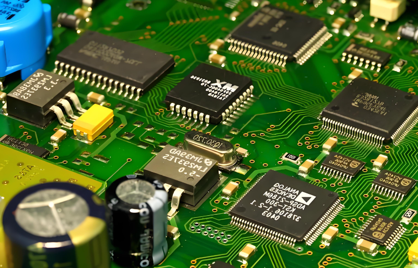
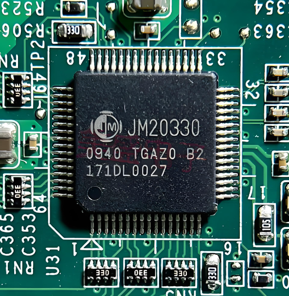
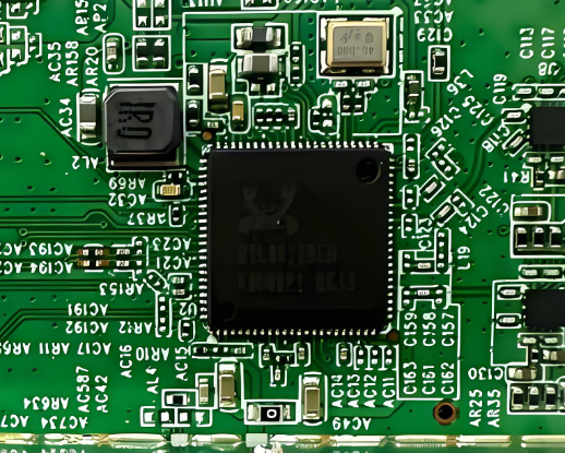
Automotive PCBA is the engineered backbone of modern vehicles, integrating complex circuitry to control everything from infotainment to advanced driver-assistance systems (ADAS). This article explores the critical standards, manufacturing excellence, and partnership criteria essential for sourcing reliable automotive printed circuit board assemblies.
Choosing the wrong automotive PCBA supplier exposes OEMs and Tier-1s to hidden risks that directly impact safety, timelines, and total lifecycle cost.
- Reliability failures: Breakdowns under heat, vibration, or humidity.
- Inconsistent quality: Weak traceability limits root-cause analysis.
- Slow qualification: IATF 16949 and automotive approvals drag on.
- Supply chain risk: Poor responsiveness across global programs.
- Escalating costs: Rework and field failures inflate liability.
These risks are mitigated by working with an automotive PCBA partner that embeds control, traceability, and quality discipline into every production stage.
- Harsh-environment testing: Thermal cycling, vibration, HALT/HASS.
- End-to-end traceability: Component-to-board barcode or RFID tracking.
- Automotive frameworks: APQP, PPAP, and FMEA from program start.
- Engineering partnership: Dedicated support and clear communication.
- Process discipline: DFM analysis and SPC to prevent defects early.
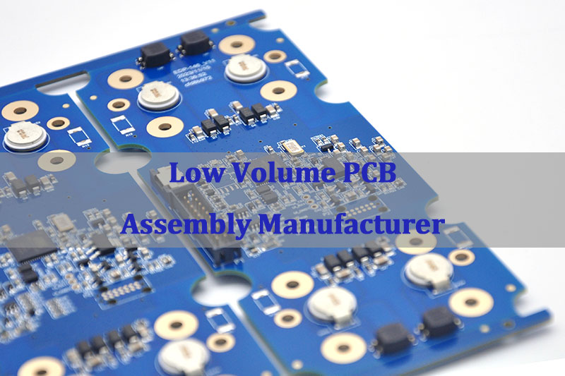
At EBest Circuit (Best Technology), we specialize in being your trusted automotive PCBA partner. As an IATF 16949 certified automotive PCBA manufacturer, we combine advanced process control with full material and production traceability to deliver high-reliability automotive electronics PCBA. Our expertise ensures your designs meet the stringent demands of the automotive industry. To review your technical requirements in detail, contact our team anytime at sales@bestpcbs.com.

Top 10 Automotive PCBA Factories
Selecting a factory requires evaluating technical capability, quality certification, and automotive focus. Here are ten leading global manufacturers known for their expertise in automotive PCBA assembly.
- Flex Ltd.: A global leader in sketch-to-scale solutions, with extensive automotive PCBA factories worldwide and deep expertise in EV and ADAS systems.
- Jabil Inc.: Offers comprehensive supply chain and manufacturing solutions for automotive, strong in electrification and connectivity PCBA automotive applications.
- Sanmina Corporation: Provides high-mix, low-to-high volume manufacturing with a focus on complex, high-reliability automotive electronics PCBA.
- Benchmark Electronics: Specializes in engineering and manufacturing for demanding sectors, including advanced automotive PCBA for engine control units.
- Venture Corporation: A leading provider of technology solutions, with strong capabilities in multilayer automotive PCBA production for sensing and control modules.
- Zollner Elektronik AG: A German-based specialist in automotive-grade PCBA, known for rigorous quality and serving premium European OEMs.
- Kimball Electronics Inc.: An IATF 16949 certified manufacturer focused on durable electronics, with a robust portfolio in automotive sensing and lighting.
- SIIX Corporation: A Japanese electronics company with a strong focus on quality and miniaturization for automotive components.
- EBest Circuit (Best Technology): A specialized automotive PCBA manufacturer and trusted automotive PCBA partner emphasizing full traceability, process control, and rapid prototyping for complex boards.
- Würth Elektronik eiSos Group: Known as a component supplier, it also offers automotive PCBA solutions through its manufacturing services, especially for PCB-based assemblies.
The ideal factory choice depends on specific program needs, but leaders are distinguished by automotive-specific certifications, proven reliability, and technological depth.

How Does Automotive PCBA Assembly Ensure Reliability Under Harsh Conditions?
Automotive electronics face extreme temperatures, constant vibration, and potential moisture ingress. Reliability is engineered through a multi-layered approach in assembly and testing.
- Material Selection: Using high-Tg laminates, automotive-grade components, and specialized conformal coatings to withstand thermal stress and corrosion.
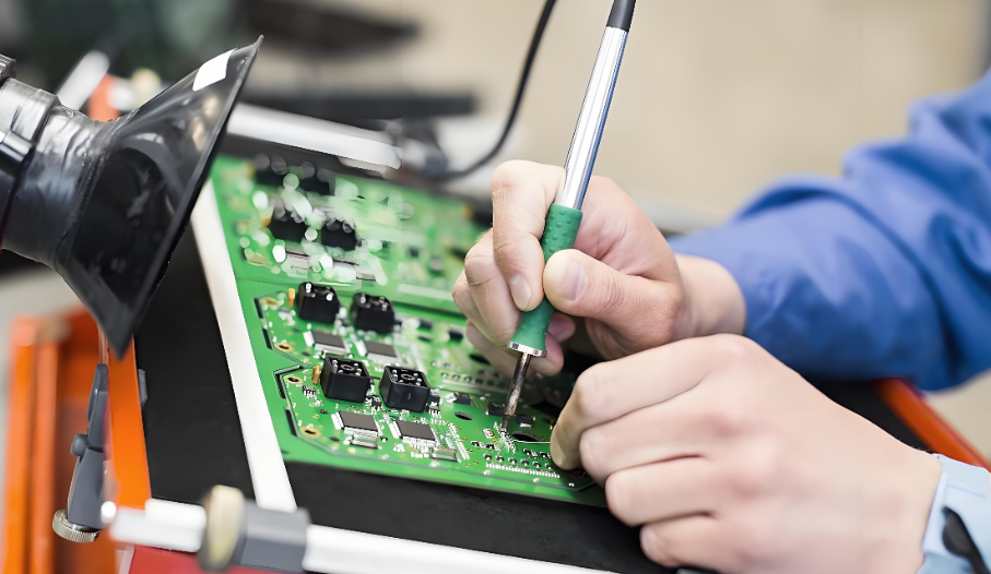
- Robust Soldering Processes: Controlled reflow soldering profiles and selective soldering ensure strong, void-free interconnections resistant to fatigue.
- Conformal Coating: Applying acrylic, silicone, or polyurethane coatings protects the automotive PCBA from humidity, dust, and chemical contaminants.
- Advanced Testing Regimes: Reliability is validated through:
- Thermal Cycling: Subjecting boards to extreme temperature swings.
- Vibration & Shock Testing: Simulating years of road conditions.
- HALT/HASS: Highly Accelerated Life/Stress Screening to find design and process weaknesses early.
- Mechanical Securement: Strategic use of brackets, adhesives, and potting to anchor components and boards against vibration.
Through this systematic combination of design, material science, and validation, automotive PCBA assembly delivers the durability required for vehicle lifespans.
Which Automotive PCBA Materials Content Meets Automotive Compliance Standards?
Compliance is non-negotiable, governed by regulations like RoHS, REACH, and the automotive-specific GADSL (Global Automotive Declarable Substance List).
- Base Laminate: Must be AEC-Q100 qualified. High-Tg FR-4 (Tg > 150°C) or specialized materials like polyimide are common for under-hood applications.
- Copper & Surface Finish: Electroless Nickel Immersion Gold (ENIG) or Immersion Silver offer reliable, lead-free solderability and surface durability.
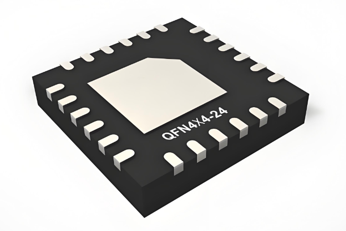
- Components: All active and passive components should be rated for automotive temperature ranges (e.g., -40°C to +125°C or higher).
- Solders & Pastes: Use of halogen-free, automotive-grade solder paste with proper alloy composition (e.g., SAC305) is standard.
- Declarable Substances: A rigorous automotive PCBA materials content gadsl declaration from the manufacturer is essential. This documents the absence or controlled use of substances like lead, cadmium, mercury, and certain phthalates.
Partnering with an automotive PCBA supplier that provides full material declarations and understands the evolving regulatory landscape is critical for compliance.
Why Is IATF 16949 Certified Automotive PCBA Critical For OEM Programs?
IATF 16949 is the definitive quality management standard for the automotive industry, extending beyond ISO 9001.
- Mandatory for OEM & Tier-1 Supply: Most major automakers require this certification for direct suppliers.
- Focus on Defect Prevention: It mandates core quality tools like Advanced Product Quality Planning (APQP) and Production Part Approval Process (PPAP), ensuring issues are resolved before mass production.
- Risk Management: Requires Failure Mode and Effects Analysis (FMEA) to proactively identify and mitigate potential automotive PCBA failure risks.
- Continuous Improvement: Embeds a culture of ongoing quality and efficiency improvements (Kaizen).
- Supply Chain Confidence: An IATF 16949 certified automotive PCBA manufacturer demonstrates a systemic commitment to automotive-quality processes, reducing audit burden and program risk.
This certification is a fundamental prerequisite, not just a badge, for any serious automotive PCBA manufacturer.
How Are Automotive PCBA Failure Risks Identified And Controlled In Production?
Proactive risk control is central to automotive manufacturing. The process is systematic and integrated.
- Design Stage (DFMEA): Potential design-related failures are analyzed and mitigated through robust PCBA requirements for automotive electronic design.
- Process Stage (PFMEA): Every manufacturing step is analyzed for potential errors (e.g., solder defects, misplacement), and controls are put in place.
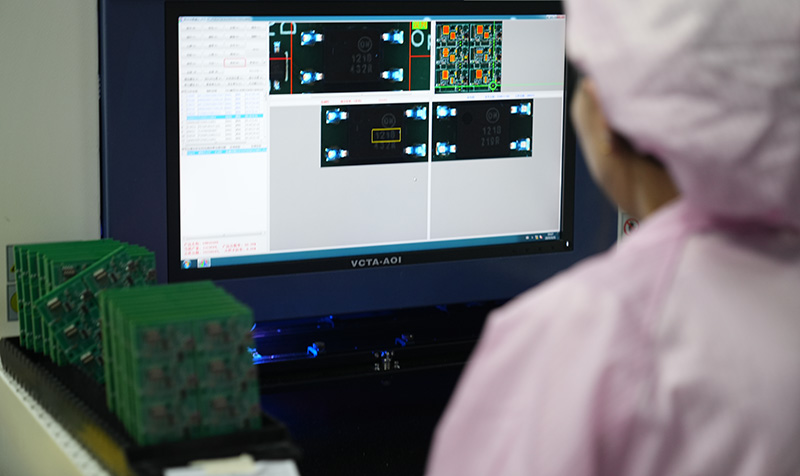
- In-Line Automated Optical Inspection (AOI): 100% post-solder inspection catches soldering, component placement, and polarity defects.
- In-Circuit Test (ICT) & Functional Test (FCT): ICT verifies component presence, value, and connectivity. FCT validates the board performs its intended function under simulated operating conditions.
- Process Control & Traceability: SPC charts monitor key process parameters (e.g., solder paste height). Full traceability links every board to its specific materials, machine parameters, and test results, enabling instant containment and root-cause analysis if an anomaly is found.
This layered approach transforms failure risk from an unknown into a managed variable.
What Makes A Trusted Automotive PCBA Partner For Global Supply Chains?
Beyond technical capability, a true partner provides strategic value and stability.
- Proven Technical & Quality Credentials: IATF 16949 certification and a portfolio of successful automotive projects.
- Transparent Communication & Responsiveness: Dedicated project management and engineering support that acts as an extension of your team.
- Supply Chain Resilience: Multi-sourced component strategies and inventory management to mitigate shortages.
- Full Data & Traceability Access: Providing clear, actionable data on yield, test results, and material history for every shipment.
- Collaborative Problem-Solving: Engaging early in the design phase for DFM analysis and working jointly to resolve any production challenges.
A trusted automotive PCBA partner like EBest Circuit (Best Technology) aligns its success with yours, ensuring a smooth, reliable journey from prototype to volume production.
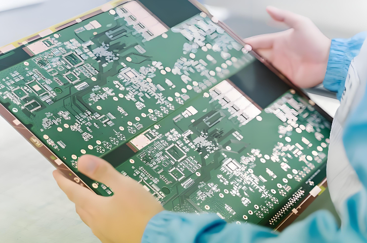
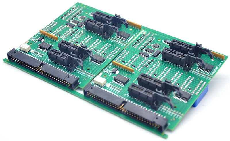
How Does Multilayer Automotive PCBA Production Support Advanced Vehicle Systems?
Modern vehicle systems (ADAS, EV powertrains, 5G telematics) demand high density, signal integrity, and power handling, which multilayer PCBs provide.
- Increased Circuit Density: Multiple layers allow for more complex routing in a smaller footprint, crucial for compact engine control units.
- Dedicated Power & Ground Planes: Improve power delivery stability and reduce electromagnetic interference (EMI), essential for high-speed digital and RF circuits like 5G automotive PCBA.
- Enhanced Signal Integrity: Controlled impedance routing on inner layers protects sensitive high-speed signals from noise.
- Improved Thermal Management: Thermal vias and embedded copper planes help dissipate heat from high-power components.
- Design Flexibility: Allows for partitioning of analog, digital, and power circuits to minimize cross-talk.
Multilayer automotive PCBA production is a specialized capability that enables the sophisticated electronics at the heart of next-generation vehicles.
Why Choose EBest Circuit (Best Technology) as Your High-Reliability Automotive Electronics PCBA Supplier?
EBest Circuit (Best Technology) focuses on controlling the real risks behind automotive electronics programs, not on generic capability statements.
- Automotive-focused systems: PCBA processes built around IATF 16949, with controlled documentation and OEM-aligned governance.
- MES-based traceability: End-to-end tracking of materials, processes, inspections, and test data for auditability and root-cause analysis.
- Engineering-driven DFM: Early DFM and feasibility reviews to reduce design risk and improve production stability.
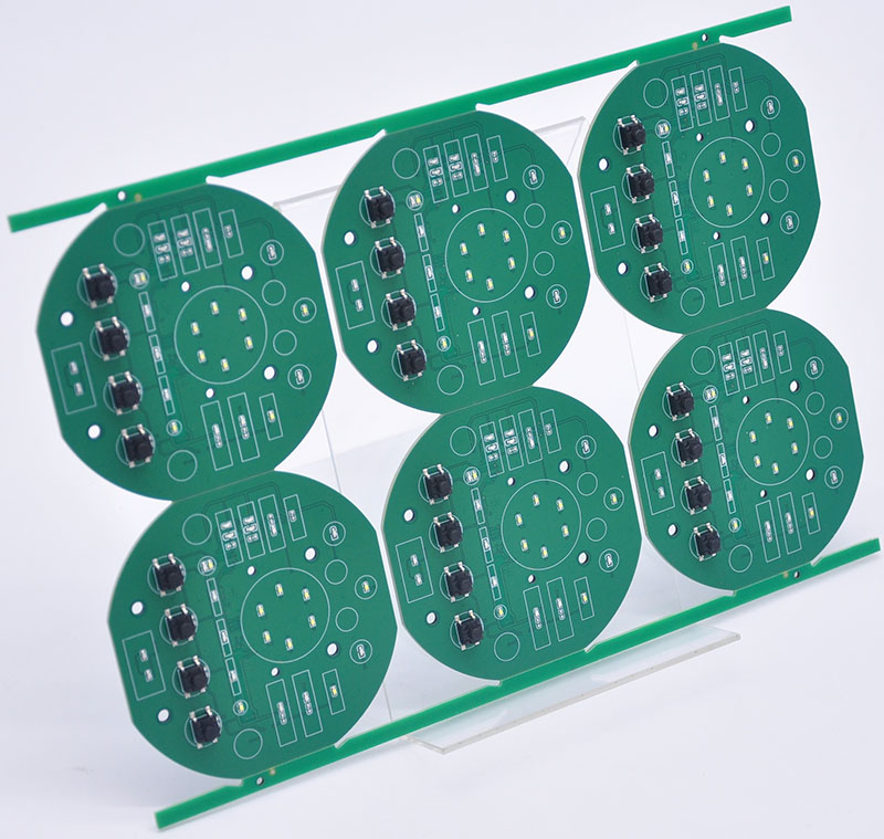
- Prototype to volume support: Small-batch builds for R&D validation, scaling smoothly to wholesale automotive PCBA production.
- Controlled scalability: SPC and change management ensure consistent quality as volumes increase.
- Partnership mindset: Transparent communication and responsive engineering support across the full product lifecycle.
For OEMs and Tier-1 suppliers requiring high-reliability automotive electronics PCBA, EBest Circuit (Best Technology) delivers a stable, traceable, and engineering-led manufacturing foundation.

In a nutshell, automotive PCBA is the critical, intelligent nexus that powers vehicle innovation, demanding unwavering reliability and compliance. This article has outlined the essential standards, manufacturing controls, and partnership qualities required to navigate this complex field. EBest Circuit (Best Technology) embodies this principle as your trusted automotive SMT partner, delivering high-reliability automotive electronics PCBA through full traceability and process control. For your next project, contact our experts at sales@bestpcbs.com.
FAQs
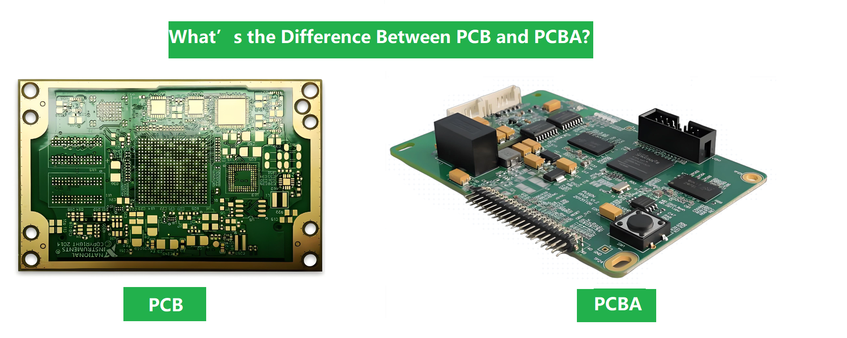
What’s the difference between PCBA and PCB?
A PCB (Printed Circuit Board) is the bare, unpopulated board. A PCBA (Printed Circuit Board Assembly) is the completed board with all electronic components soldered onto it.
What is PCB in automotive?
In automotive contexts, a PCB is the foundational substrate for electronic control units (ECUs), sensors, infotainment systems, and lighting controllers. Automotive PCBA refers to the fully assembled, tested, and often conformally coated unit ready for integration into a vehicle.
How many types of PCBA are there?
Types are primarily defined by the PCB used: single-sided, double-sided, multilayer (4+ layers), HDI (High-Density Interconnect), rigid, flex, and rigid-flex PCBA. Automotive applications frequently use complex multilayer, HDI, or rigid-flex assemblies.