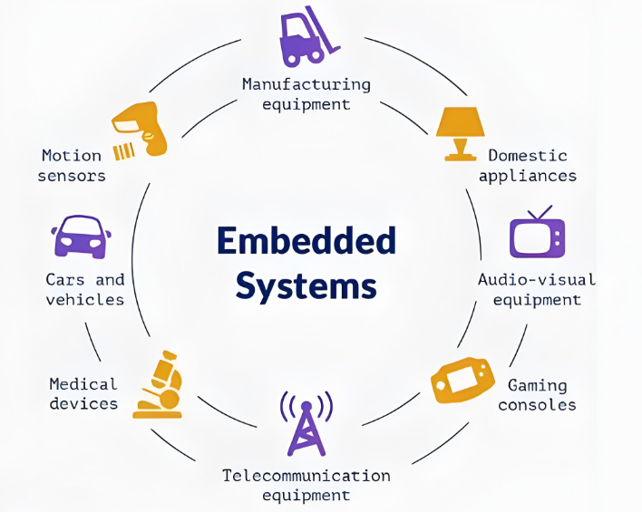
Embedded systems are at the core of modern technology, enabling devices to interact with their environment in intelligent ways. These systems rely on sensors to collect real-world data and use microcontrollers to process and respond to that data. From smart homes to industrial automation, embedded systems play a vital role in optimizing efficiency and automation.

What is a Sensor in an Embedded System?
A sensor in an embedded system is a device that detects and measures physical properties such as temperature, pressure, motion, or light and converts them into electrical signals. These signals are then interpreted by a microcontroller or processor to make real-time decisions.
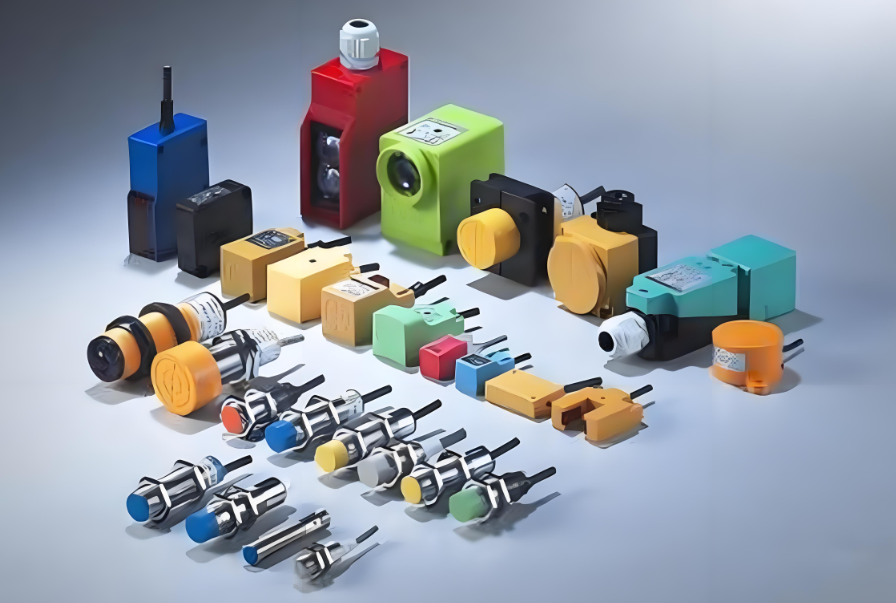
Sensors serve as the system’s primary interface with the external environment. They can measure a wide range of physical and chemical properties, including:
- Temperature (e.g., Thermocouples, RTDs, Thermistors)
- Pressure (e.g., Barometers, Strain Gauges, MEMS Pressure Sensors)
- Light (e.g., Photodiodes, LDRs, IR Sensors)
- Motion (e.g., Accelerometers, Gyroscopes, PIR Sensors)
- Sound (e.g., Microphones, Ultrasonic Sensors)
- Gas & Chemical Composition (e.g., Gas Sensors, pH Sensors)
For example, in an air conditioning system, a temperature sensor detects the room’s temperature. The embedded system processes this data and adjusts the cooling settings accordingly. Similarly, in a smartphone, an accelerometer detects movement and rotates the screen based on the phone’s orientation.
What Are the Four Main Types of Sensors?
Sensors come in various types, but they can be categorized into four primary groups based on the type of data they collect.
1. Temperature Sensors
These sensors measure heat levels and are widely used in industrial automation, healthcare, and consumer electronics.
- Examples: Thermocouples, Resistance Temperature Detectors (RTDs), and thermistors.
- Applications: Air conditioners, refrigerators, and medical devices like digital thermometers.
2. Pressure Sensors
Pressure sensors detect force exerted on a surface and convert it into an electrical signal. They are essential in automotive and industrial applications.
- Examples: Strain gauge sensors, piezoelectric sensors, and capacitive pressure sensors.
- Applications: Tire pressure monitoring in vehicles, fluid pressure measurement in pipelines.
3. Motion Sensors
Motion sensors detect movement and acceleration. They are used in security systems, gaming controllers, and wearable devices.
- Examples: Accelerometers, gyroscopes, and infrared sensors.
- Applications: Fitness trackers, anti-theft alarms, and robotic systems.
4. Optical Sensors
Optical sensors detect light intensity and are widely used in smartphones, industrial automation, and medical diagnostics.
- Examples: Photodiodes, infrared sensors, and laser sensors.
- Applications: Touchscreen devices, barcode scanners, and heart rate monitors.
What Is the Role of Sensors in Embedded Systems?
Sensors act as the eyes and ears of embedded systems. They detect physical changes such as temperature shifts, pressure variations, motion, or light intensity and convert them into signals the system can process. Key functions of sensors in embedded systems including:
- Continuous Data Collection: Sensors provide real-time information, helping systems monitor environmental conditions accurately.
- Automation and Control: Embedded systems use sensor data to adjust operations without human intervention, improving efficiency.
- Safety and Protection: In applications like automotive airbags or fire alarm systems, sensors trigger responses that enhance safety.
- Energy Optimization: Smart lighting, climate control, and industrial processes rely on sensors to reduce energy waste.
Without sensors, embedded systems would not be able to interact with their surroundings, making them essential for smart technology.
How Sensors Are Integrated into Embedded Systems?
How to embedded system interact with various sensors? Integrating sensors into embedded systems involves multiple steps, from selecting the right sensor to processing its data for decision-making. Let’s see how they integrated into embedded systems:
1. Selecting the Right Sensor
The first step in sensor integration is choosing the appropriate sensor based on the system’s requirements. Key factors to consider include:
- Type of Measurement: Sensors detect parameters like temperature, pressure, motion, or humidity.
- Accuracy and Sensitivity: Higher precision is needed in applications like medical devices, while industrial sensors prioritize durability.
- Power Consumption: Battery-operated systems require low-power sensors to enhance efficiency.
- Communication Interface: Sensors use protocols like I2C, SPI, UART, or analog output to transmit data.
Selecting the right sensor ensures optimal system performance and reliability.
2. Connecting Sensors to the Embedded System
Once the sensor is selected, it needs to be physically connected to the embedded system. The connection type depends on whether the sensor is analog or digital.
- Analog Sensors: These sensors provide continuous voltage signals that vary based on detected parameters. An Analog-to-Digital Converter (ADC) is required to process the signal.
- Digital Sensors: These sensors transmit data in binary form (0s and 1s) and can be directly connected to microcontrollers using interfaces like I2C, SPI, or UART.
3. Sensor Calibration and Signal Conditioning
Before using sensor data, calibration and signal conditioning are necessary to improve accuracy and reliability. Calibration process is by adjusting sensor readings to match standard measurements. For example, temperature sensors need calibration against a known temperature source.
4. Data Processing in Microcontrollers
In the embedded system, the microcontroller acts as the brain of the embedded system, processing data from sensors and executing predefined tasks.
- Raw Data Conversion: If the sensor provides an analog output, the ADC (Analog-to-Digital Converter) converts it into a digital signal for processing.
- Data Filtering: Algorithms help remove errors or fluctuations from sensor readings.
- Decision-Making: The system processes data and triggers appropriate actions. For example, a temperature sensor in an HVAC system adjusts cooling or heating based on detected temperatures.
5. Communication Between Sensors and Embedded Systems
Embedded systems use communication protocols to exchange data between sensors, microcontrollers, and external devices. Commonly used are:
- I2C (Inter-Integrated Circuit): Commonly used for connecting multiple low-speed sensors with minimal wiring.
- SPI (Serial Peripheral Interface): Provides faster data transfer, suitable for high-speed applications like industrial automation.
- UART (Universal Asynchronous Receiver-Transmitter): Used in GPS modules, wireless communication, and serial interfaces.
- Wireless Communication: Some sensors use Wi-Fi, Bluetooth, or Zigbee for remote data transmission, seen in smart home and IoT applications.
What Is the Difference Between an Embedded System and a Microcontroller?
Many people may confused about embedded system and microcontroller, they think they are the two different system. Actually, a microcontroller is just one part of an embedded system. The embedded system includes the microcontroller, sensors, actuators, and other components. Their key differences are listing as below:
| Feature | Embedded System | Microcontroller |
| Definition | A complete system that includes a microcontroller, sensors, and actuators | A small chip that processes data |
| Components | Sensors, microcontroller, actuators, memory, and power supply | CPU, RAM, ROM, and I/O ports |
| Function | Performs dedicated tasks like monitoring temperature or controlling motors | Executes instructions and controls peripherals |
| Examples | Smart home systems, medical monitors, industrial robots | ATmega328, PIC16F877A |
How Do Microcontrollers Interact with Sensors and Actuators in an Embedded System?
Microcontrollers serve as the core of embedded systems, handling communication between sensors and actuators. Sensors collect real-world data such as temperature, motion, or pressure and send it to the microcontroller for processing. Based on this data, the microcontroller makes decisions and controls actuators to perform specific actions.
1. Receiving Data from Sensors
Sensors generate signals, either analog or digital, which the microcontroller processes:
- Analog Sensors: Provide variable voltage signals that require an Analog-to-Digital Converter (ADC) to convert them into digital values.
- Digital Sensors: Directly transmit binary data via communication protocols like I2C, SPI, or UART for faster processing.
2. Processing Sensor Data
The microcontroller processes raw sensor readings using filtering, calibration, and decision-making algorithms. It can also store data for further analysis or send it to external systems via wired or wireless communication.
3. Controlling Actuators
After analyzing sensor data, the microcontroller sends control signals to actuators, which convert electrical signals into physical actions. Common actuators include:
- Motors: Used in robotic arms, conveyor belts, and automated vehicles.
- Relays: Switch electrical circuits on or off, commonly found in home automation.
- Solenoids: Control fluid flow in valves and hydraulic systems.
4. Feedback and Closed-Loop Control
Many embedded systems use a closed-loop control system, where sensors provide continuous feedback to the microcontroller. This ensures precise actuator adjustments based on real-time data. For example, in an HVAC system, a temperature sensor constantly updates the microcontroller, which then adjusts the cooling or heating output.
5. Communication with External Devices
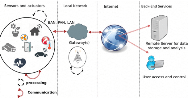
Microcontrollers often transmit sensor and actuator data to external systems using wireless communication protocols like Wi-Fi, Bluetooth, or Zigbee. This is common in IoT applications, where devices send data to cloud platforms for remote monitoring and automation.
Examples of Embedded Systems and Sensor Interactions
Embedded systems are used in various industries, with sensors playing a crucial role in automation, monitoring, and control. Below are some common examples where embedded systems interact with different types of sensors to perform real-world tasks efficiently.
1. Automotive Systems
- Wheel speed sensors detect the rotation of each wheel, and the microcontroller adjusts braking pressure to prevent skidding.
- Pressure sensors in tires continuously send data to the embedded system, alerting the driver if pressure drops below a safe level.
2. Industrial Automation
- Sensors monitor environmental conditions in manufacturing plants to maintain product quality, especially in food processing and pharmaceuticals.
- Robots use infrared and ultrasonic sensors to detect objects and avoid collisions while performing automated tasks.
3. Healthcare and Medical Devices
- Wearable devices use optical or ECG sensors to track heartbeats and detect irregularities.
- Glucose sensors in insulin pumps help diabetic patients regulate blood sugar levels automatically.
4. Smart Home Automation
- Infrared sensors detect movement, activating alarms or security cameras in case of intrusion.
- Light sensors adjust indoor lighting based on natural daylight levels, reducing energy consumption.
5. Wearable Technology
- Sensors measure heart rate, step count, and blood oxygen levels, helping users track fitness goals.
- Smart textiles with embedded sensors monitor body temperature and adjust clothing insulation accordingly.
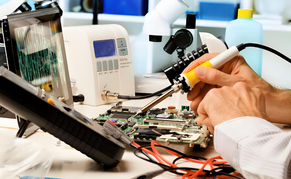
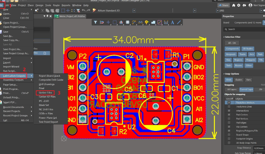
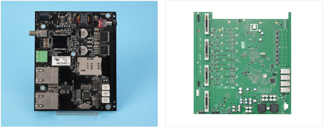
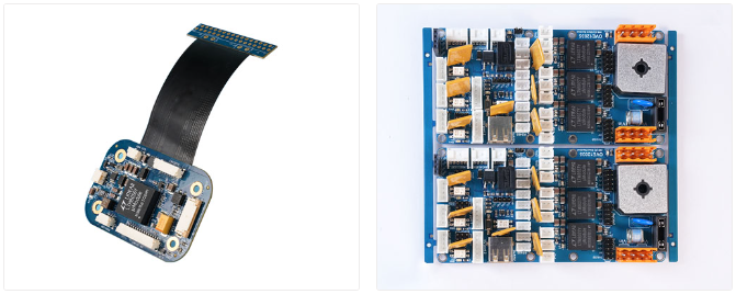
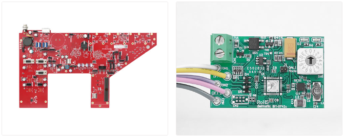
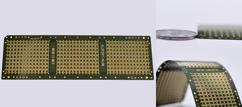
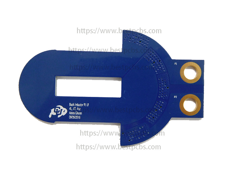
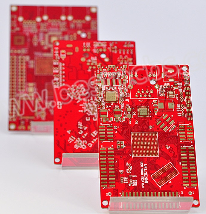
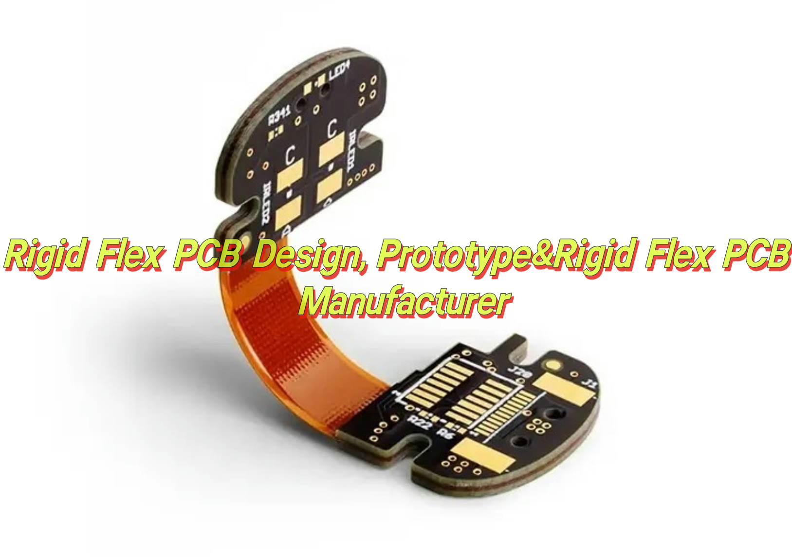
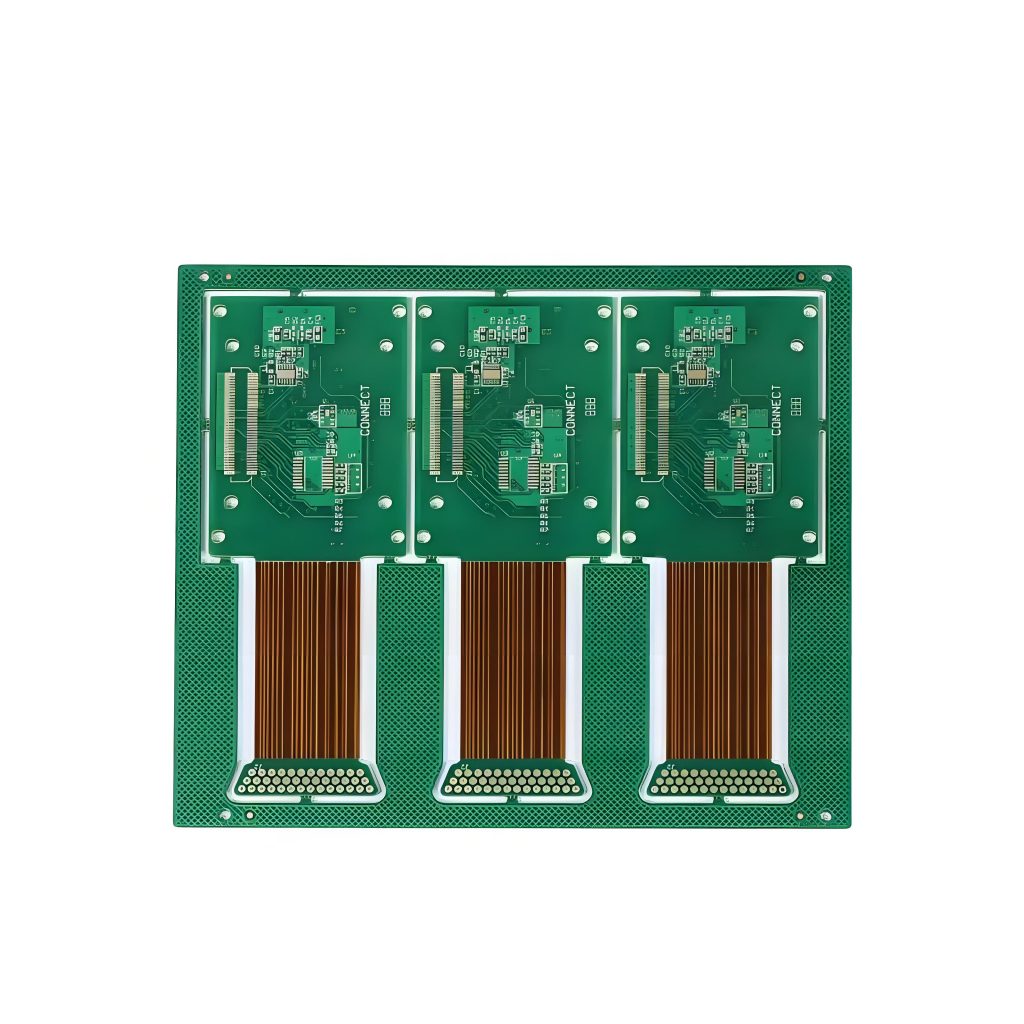
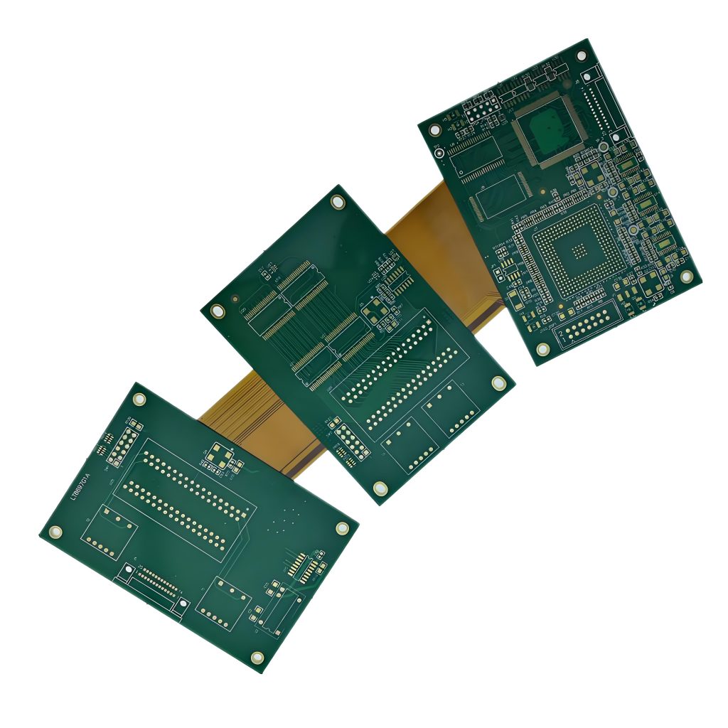
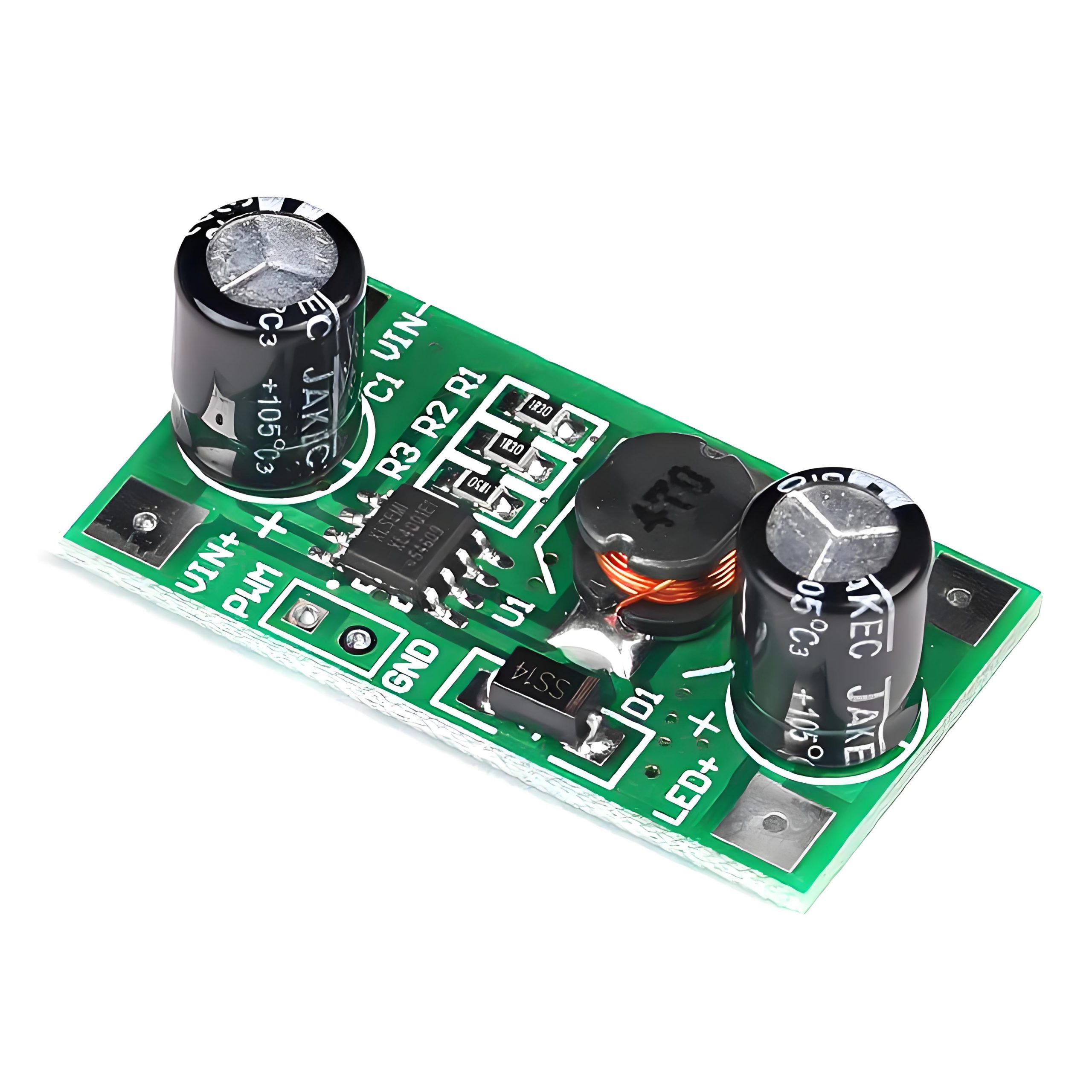
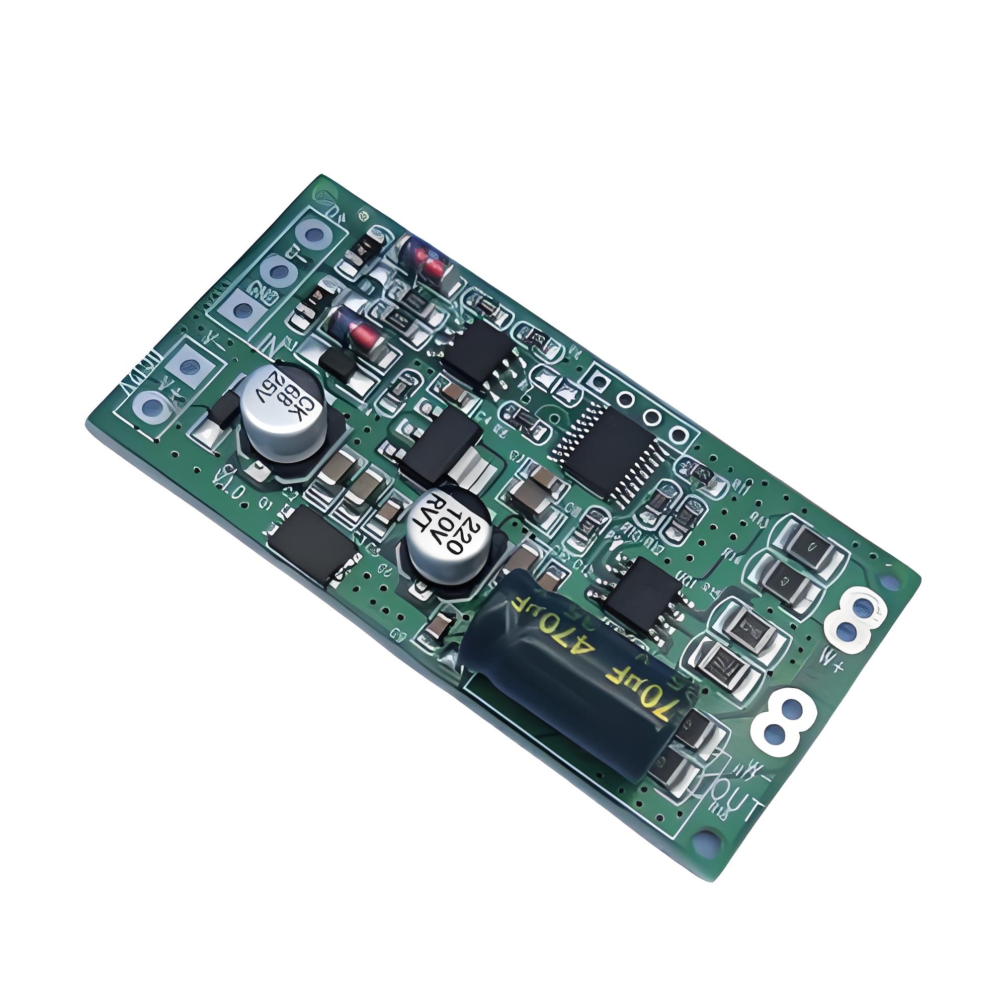
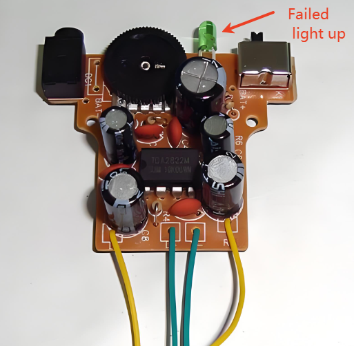
One-Stop PCB & PCBA Manufacturer for Embedded Systems
After understanding how the embedded system interacts with the sensors and finalizing your project design, are you looking for an one-stop PCB manufacturer to make it into reality? If you are doing this, then do not hesitate to contact EBest Circuit (Best Technology).
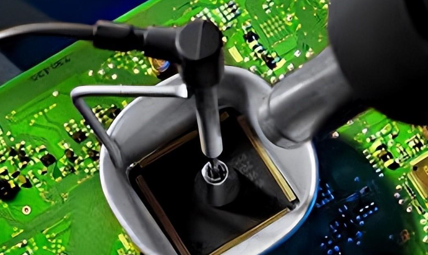
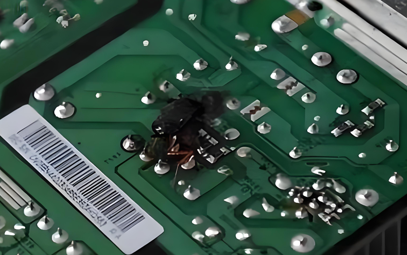
Since established in 2006, we have worked in PCB & PCBA for more than 18 years, during these years, we have accumulated much experience to overcome numerous difficulties in the manufacturing. We have our own PCB factories in Shenzhen, including FR4 PCB, metal core PCB, ceramic PCB, flex & rigid flex PCB. And to serve customer better, we built PCBA factory both in China and Vietnam, each has more than 3 SMT lines and equipped with advanced pick and place aseembly machines. In addtion to this, we offer box building assembly service for embedded systems. Providing full turn-key service from PCB design, PCB fabricating, components sourcing, IC programing, pcb assembly, function testing… If you are interested in it, you are welcome to e-mail us at sales@bestpcbs.com. Our team will try their best to help you!