With the development of LED technology, LED power keeps increasing. This is closely related to heat dissipation. In order to resolve heat dissipation of LED with big power, aluminum-based copper-clad laminate is highly applied in led strip field.
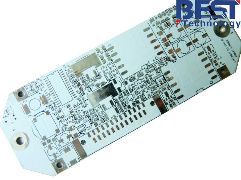
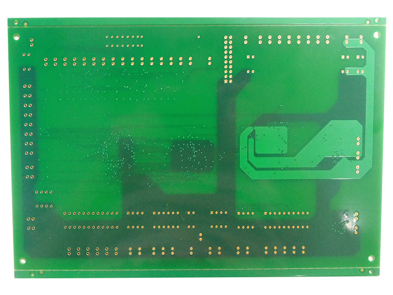
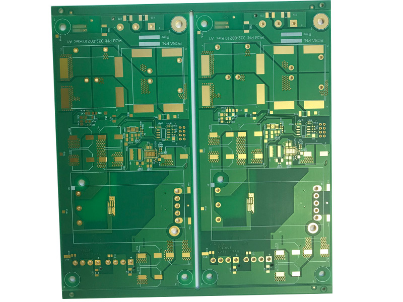
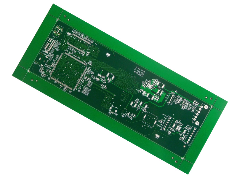
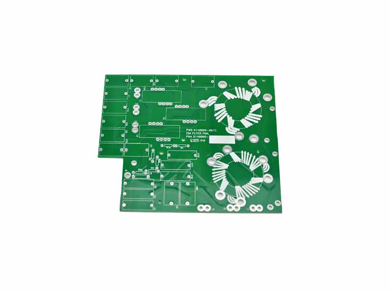
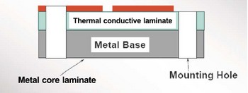
Aluminum PCB(metal-based heat dissipation board) is a kind of unique metal-based copper-clad laminate. It has good head conductivity, electrical insulation and machining performance. Single-sided aluminum pcb consists of three layers of structures:circuit layer(copper foil), insulation layer and metal-based layer. Circuit layer requires large current-carrying capability, so we should use thick copper foil(generally 35um to 280um). The insulation layer for heat conduction is the core technology of aluminum pcb. It is general composed of special polymer filled with special ceramic. Small heat resistance, excellent viscoelasticity and anti-aging are all its advantages. And it is also able to bear mechanical and heat stress. Metal-based layer is the supporting component of aluminum pcb, and it needs to have high heat conductivity, so we generally use aluminum board, or copper board(which can provide higher conductivity). And it is suitable for regular machining such as drilling, punching and cutting. Techniques include gold plating, solder levelling, osp, ENIG, lead-free ROHS and so on.
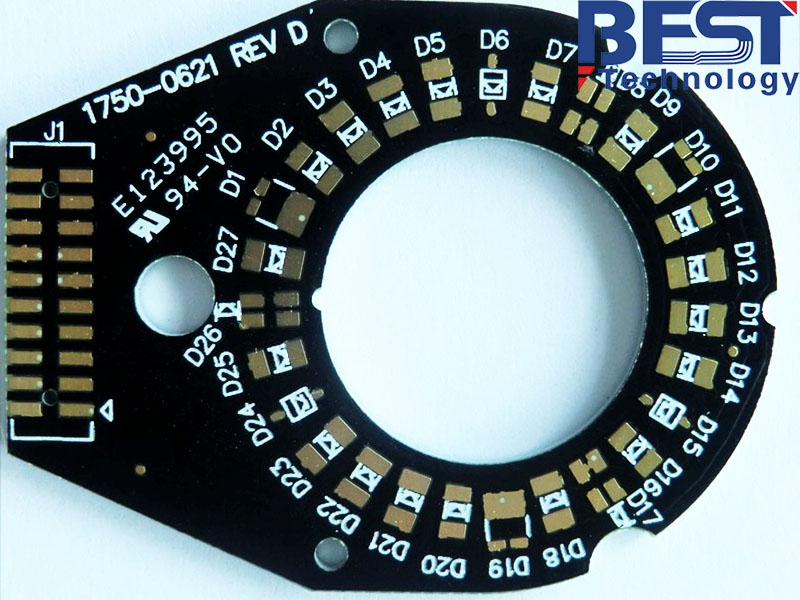
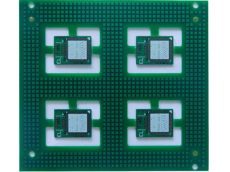
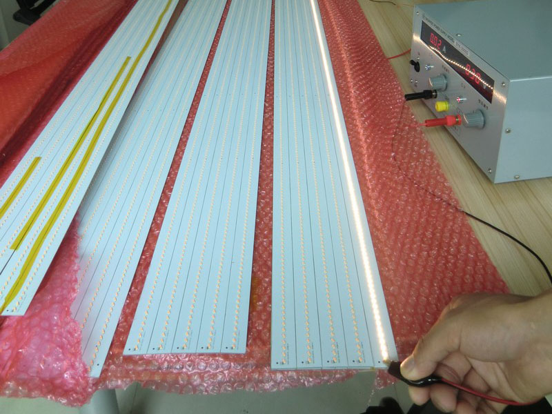
Aluminum pcb is commonly seen in LED products and has two sides(the front side and the reverse side). The white face is used to solder LED pin, and the other face presents natural color. It is generally painted with thermal conductivity paste and then contacted with heat conduction part. LED aluminum pcb is mainly used in power amplified mixed integrated circuits for STK series, motor cycles, automobile and electronics field.
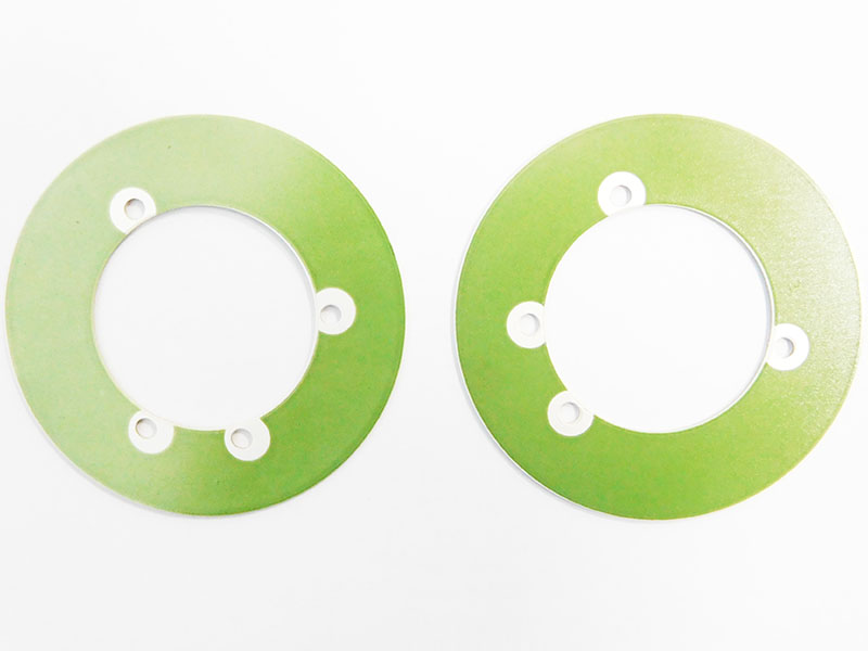
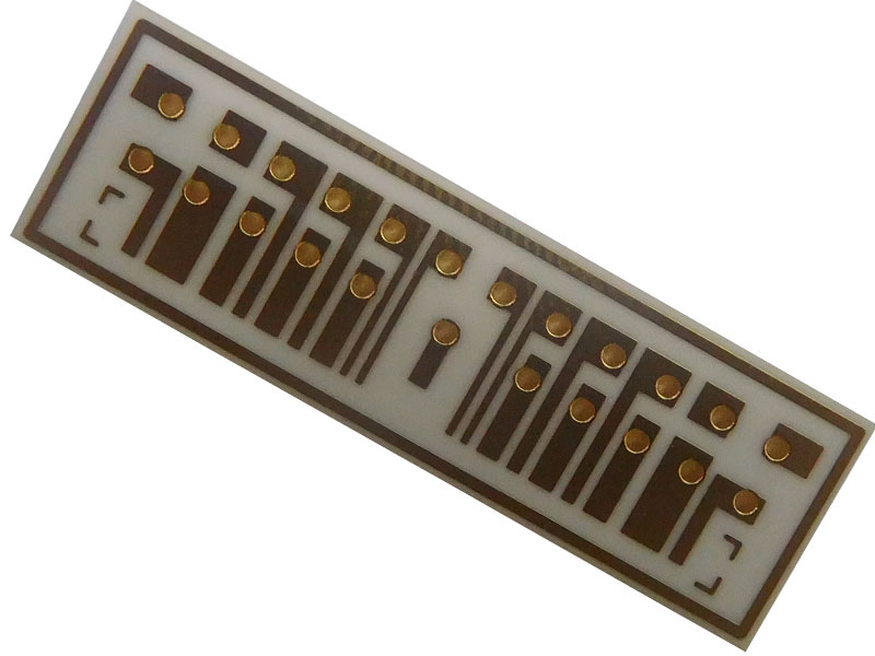
There are many kinds of aluminum pcb for led tube, which varies based on the length and width of led tube. Aluminum pcb for led tube is popular with people due to its good quality, and durable and energy-saving features.
Aluminum pcb for led tube can save electricity as high as 70%. The light intensity of 12W Led tube is equal to 40w fluorescent tube. The service life of LED tube is is more than 10 times that of general fluorescent tube. It can be free of maintenance. Also, there is no need to change LED tube, barratter and starter frequently.
Generally, fluorescent tube has high temperature inside and needs to be used for more than 10 hours everyday in most cases. This problems are perfectly resolved by aluminum pcb for led tube.
If you have any queries, comments or suggestions on aluminum pcb for led, welcome to leave your message.