How to fix a cold solder joint? Cold solder joints refer to soldering that is not fully melted due to insufficient temperature or too short a time, resulting in a rough, dull solder joint surface and unreliable connection.
The method to repair a cold solder joint is to reheat the solder joint with a soldering iron to melt and flow the solder, and add an appropriate amount of solder if necessary to ensure that the solder joint is smooth and the connection is firm.
What is a cold solder joint?
A cold solder joint occurs when a solder connection doesn’t properly melt and fuse the metal parts together. This results in a weak and unreliable electrical connection.
Soldering is meant to create a strong bond between components and their pads or leads, but if the solder fails to properly flow and cool, you get a cold joint.
A cold solder joint often happens when the joint doesn’t get hot enough to create the desired fusion between the metal parts, or when the solder doesn’t flow well due to contamination or poor technique.
As a result, the solder might look dull or cracked, and the connection won’t be stable. A cold solder joint can occur in any soldering project, from simple DIY electronics to complex PCB assembly.
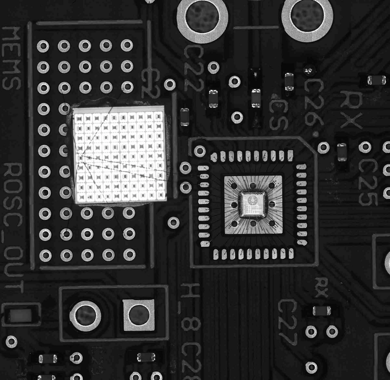
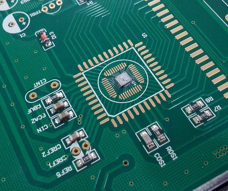
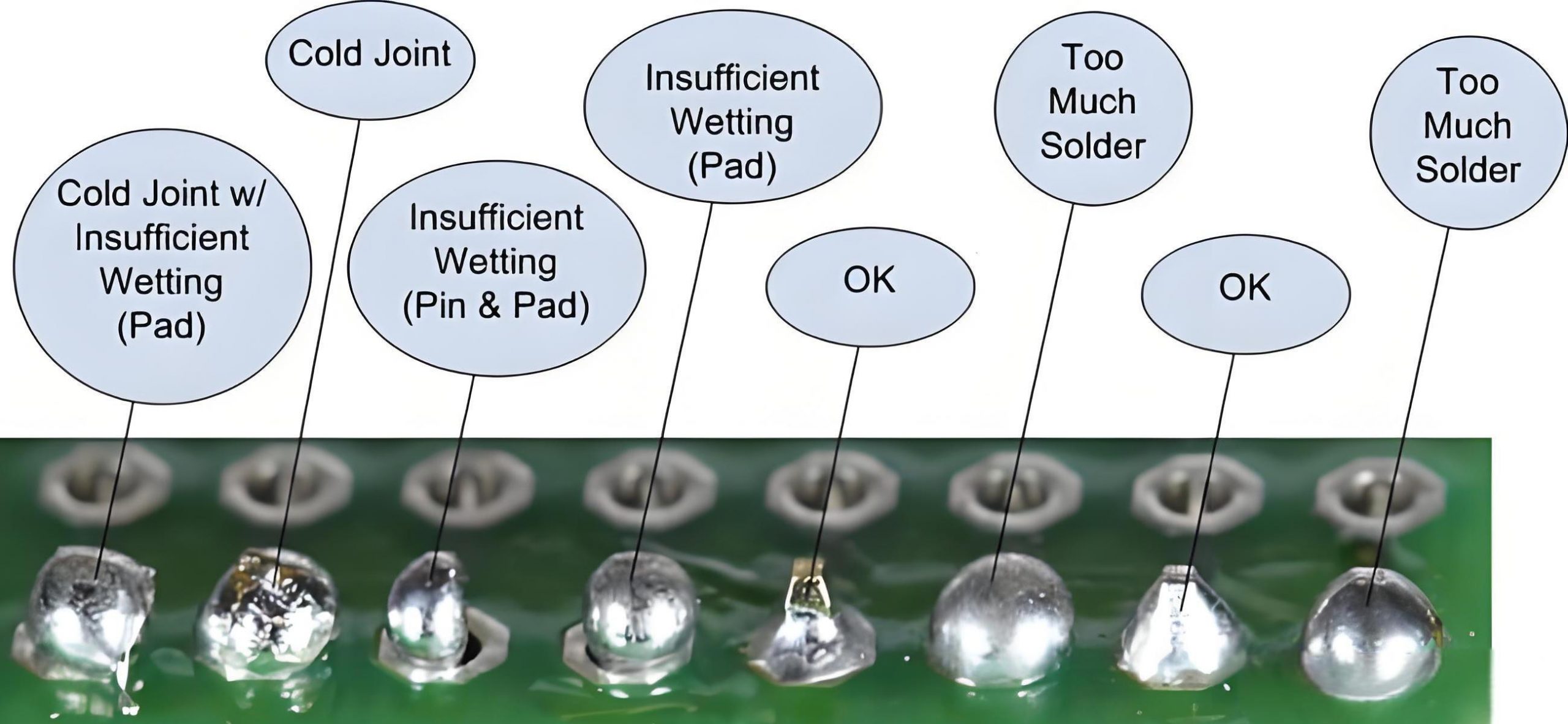
What is the characteristic appearance of a cold solder joint?
Some of the most common visual indicators of a cold joint solder include:
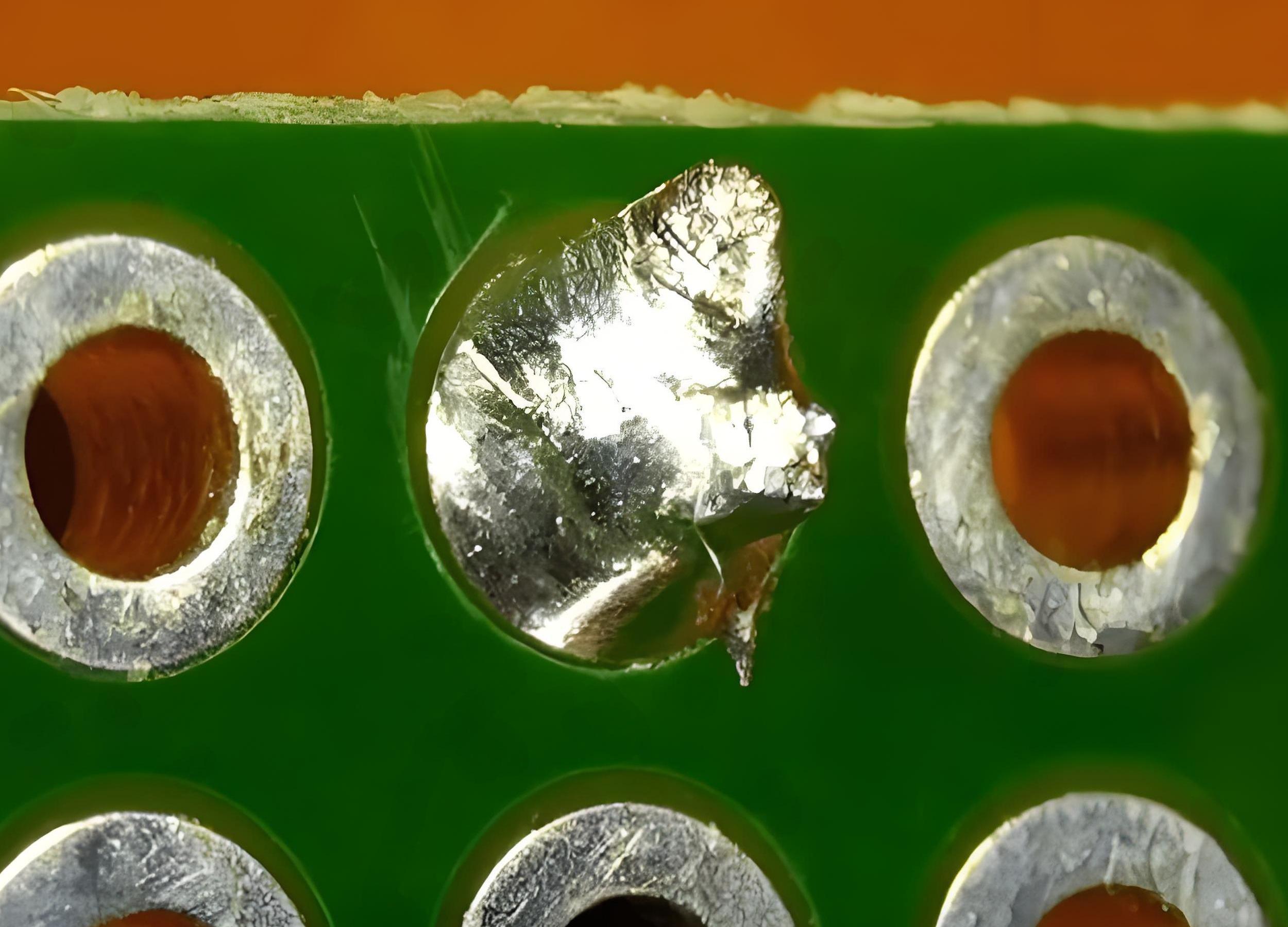
- Dull or Grainy Appearance: A healthy solder joint should have a shiny, smooth finish. In contrast, cold joints usually look dull or rough. The dullness results from poor fusion between the solder and the metal parts.
- Cracks or Gaps: Cold solder joints often have visible cracks or gaps between the solder and the components. These imperfections prevent a solid connection from forming.
- Irregular Shape: Cold solder joints may appear lumpy or uneven, rather than smooth and symmetrical. A well-soldered joint should have a uniform shape, with the solder fully covering the lead and the pad.
- No Flowing Solder: If the solder hasn’t flowed properly into the joint, you may see a lot of excess solder piled on one side, while the other side looks dry or incomplete.
When you encounter a cold solder joint, it’s vital to address it promptly, as it can cause intermittent connections or total failure of the circuit.
What are the effects of cold solder joints?
A cold solder joint can lead to several issues that can disrupt the functionality of your electronics:
- Intermittent Connections: A cold joint is unreliable and can cause intermittent electrical connections. The circuit might work only sporadically, making troubleshooting difficult.
- Circuit Failures: If the solder joint fails completely, it may lead to a total breakdown of the circuit. This can result in device malfunction, loss of data, or even short circuits in extreme cases.
- Signal Loss: In high-frequency circuits, even a small interruption in the signal path can lead to a noticeable degradation in performance, such as signal noise or data corruption.
- Overheating: Cold joints can also contribute to overheating, as the weak connection might not handle the required current, leading to excess heat and further damage to components.
In summary, cold solder joints are a significant issue that can affect the stability and reliability of your electronics. It’s important to identify and fix them before they cause more serious problems.
How to prevent a cold solder joint?
The best way to avoid cold solder joints is to ensure that you follow good soldering practices.
- Proper Heating: Always heat both the pad and the lead properly before applying solder. The solder should flow smoothly once it touches the heated area.
- Use Quality Solder: Ensure you’re using high-quality solder. The solder wire should have a proper flux core to promote good flow and prevent oxidation.
- Clean Components: Clean the components and pads before soldering to remove any oil, dust, or oxidation. This can improve the connection and reduce the risk of a cold joint.
- Right Soldering Technique: Don’t apply too much solder. The goal is to create a smooth, even connection, not a blob of excess solder. Avoid moving the component too much while the solder is cooling, as this can lead to a cold joint.
- Good Soldering Iron Tip: Make sure your soldering iron tip is clean and tinned. A dirty or oxidized tip can result in uneven heating and poor solder flow.
How to check for cold solder joints?
Checking for cold solder joints is essential to ensure that your circuit works properly. You can inspect your joints visually and perform electrical tests to confirm their integrity.
- Visual Inspection: The first step is to look closely at each solder joint. Check for dullness, cracks, irregularities, or excess solder. If the joint looks anything other than shiny and smooth, it may be a cold solder joint.
- Use a Magnifying Glass: If the soldering is delicate or you’re working with tiny components, use a magnifying glass or a microscope to inspect the joints in more detail.
- Electrical Testing: After performing a visual inspection, you can test the connection with a multimeter to check for continuity. If the multimeter shows no continuity or fluctuates, it indicates a poor connection due to a cold solder joint.
- Functional Testing: Sometimes, simply testing the functionality of the circuit can help you detect cold solder joints. If certain components fail to work or intermittently cut out, cold solder joints are often the culprit.
By regularly checking your solder joints, you can catch cold joints early and fix them before they cause problems.
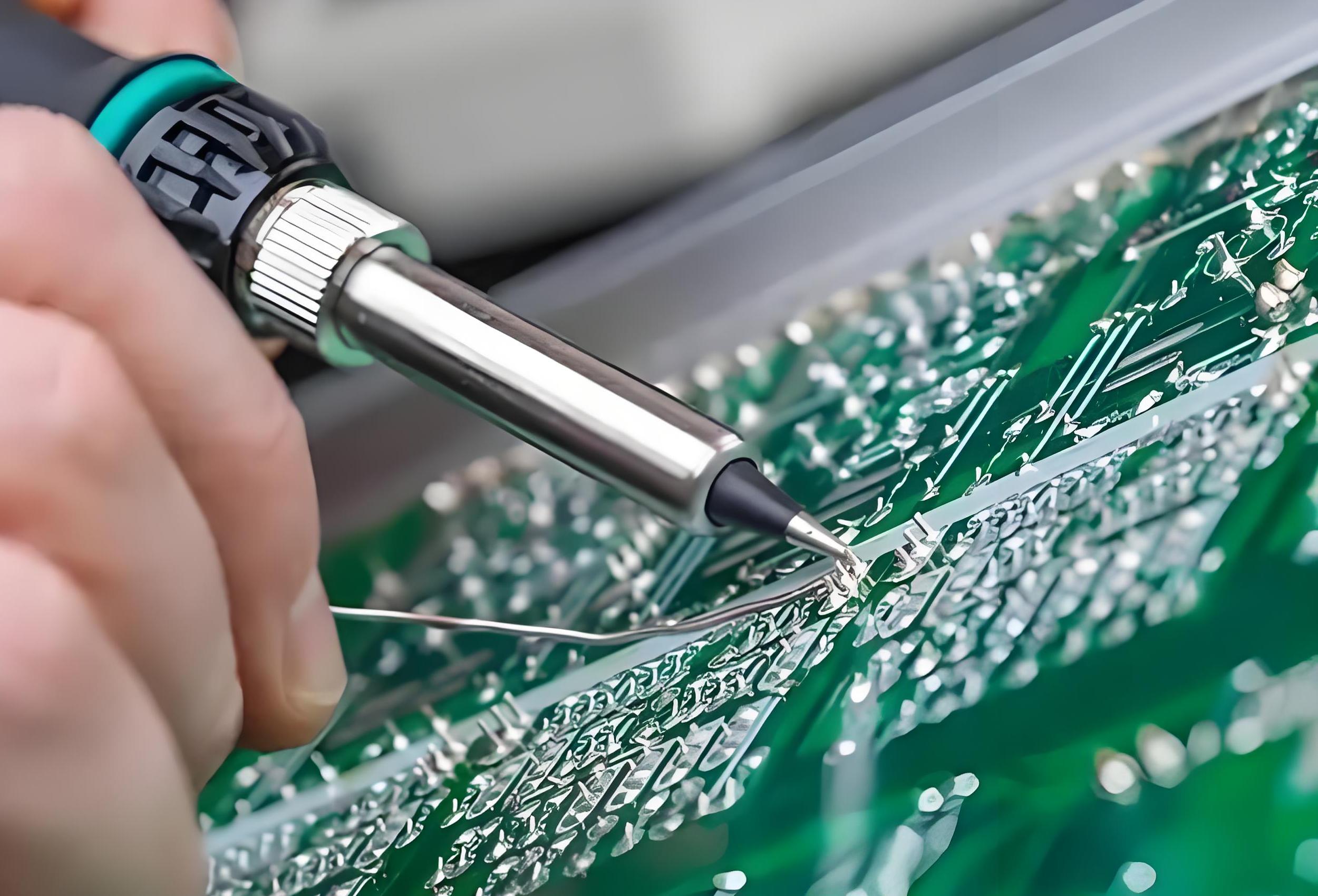
How to fix a cold solder joint?
Fixing a cold solder joint involves reflowing the solder and ensuring that the connection is strong and reliable. Here’s a step-by-step guide on how to fix it:
- Heat the Joint Again: Use your soldering iron to heat the cold solder joint. Allow the joint to heat up until the solder begins to melt. This will ensure the solder flows properly and fuses the components.
- Add New Solder: If necessary, add a small amount of fresh solder to the joint. This will help create a stronger connection. The new solder should melt and flow smoothly around the pad and lead.
- Remove Excess Solder: If there’s excess solder, use a desoldering pump or wick to remove it. Too much solder can create weak joints or cause shorts.
- Let It Cool: Once the joint is properly soldered, let it cool naturally. Avoid disturbing the joint while it cools, as this can lead to a cold joint once again.
- Check the Joint Again: After reflowing the solder, recheck the joint for a shiny appearance, good flow, and solid connection.
What is the root cause of cold solder joint?
The root causes of cold solder joints generally revolve around improper heating, poor soldering technique, or contaminated materials. Some common causes include:
- Insufficient Heat: If the soldering iron is not hot enough or if the joint isn’t heated long enough, the solder will not properly fuse, resulting in a cold joint.
- Dirty or Oxidized Components: If the components or pads are dirty or oxidized, the solder won’t adhere properly, leading to a weak bond.
- Poor Soldering Technique: Applying solder too quickly, using too little solder, or moving the components while the solder is cooling can lead to cold solder joints.
- Low-Quality Solder: Poor-quality solder may not melt properly or may have impurities, preventing the solder from flowing correctly.
How do you change a cold solder joint to a correct one?
To turn a cold solder joint into a correct, reliable one, you need to apply the correct amount of heat and solder while following proper soldering techniques. Here’s how to do it:
- Remove the Cold Joint: If the joint is completely ineffective, use a soldering iron to reflow the solder, then remove it with a desoldering pump or wick.
- Resolder the Joint: Heat the pad and lead again, then apply fresh solder and let it flow evenly.
- Test the Joint: After resoldering, test the connection for continuity to ensure that the circuit works as intended.
Conclusion:
Always make sure to follow proper soldering practices, inspect your joints carefully, and reflow any faulty connections as needed. By taking care of cold solder joints early on, you ensure the longevity and functionality of your circuits.
For professional soldering and PCB manufacturing services, EBest Circuit (Best Technology) is here to help. Reach out to us at sales@bestpcbs.com for more information.