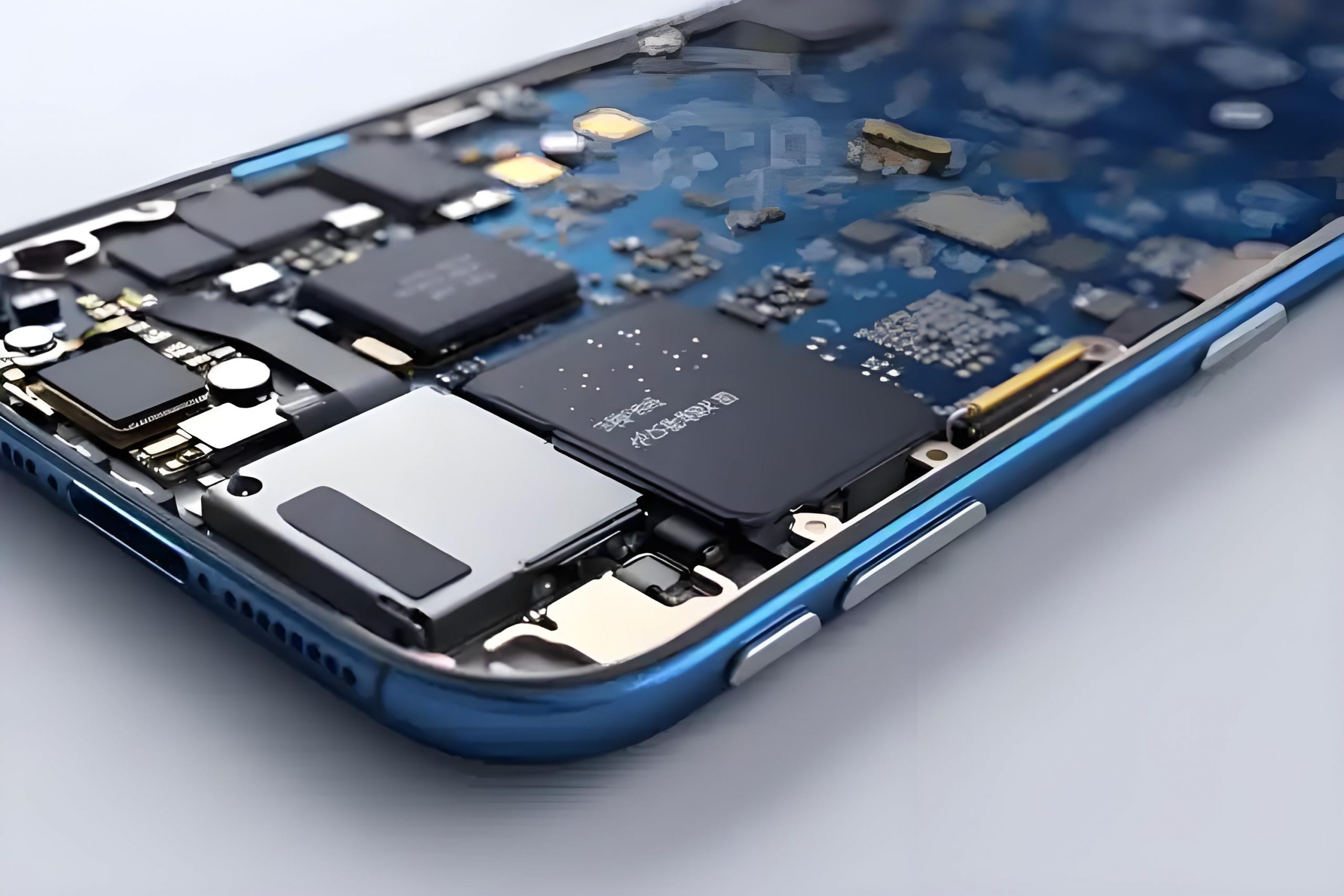
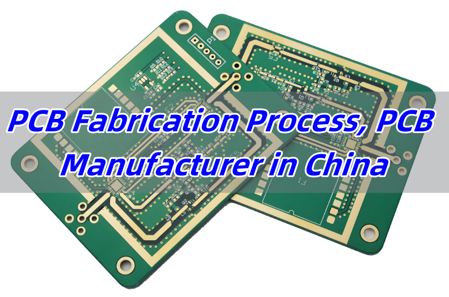
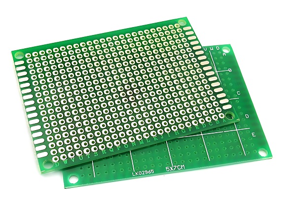
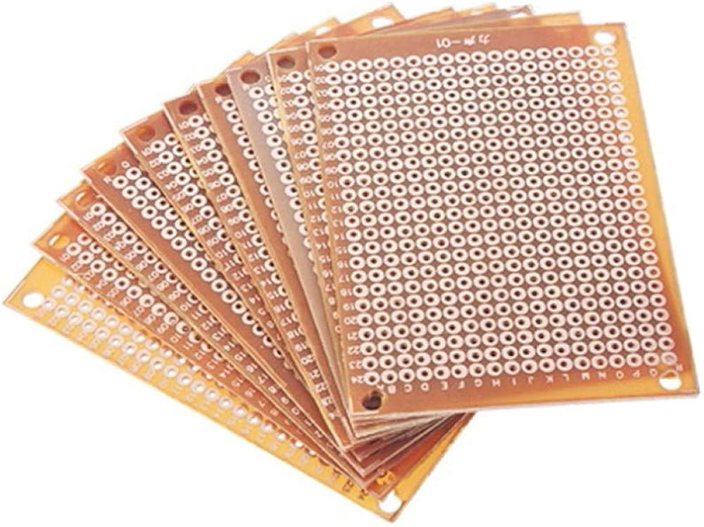
When developing new electronic products, fast and reliable prototyping is critical to success. Choosing the right partner for electronic prototype manufacturing can significantly impact your product quality, development timeline, and cost. China has become a global leader in PCB and electronics manufacturing, offering cutting-edge capabilities with competitive pricing and fast turnaround.
In this article, we’ve selected the Top 10 electronic prototype manufacturers in China based on their service quality, industry reputation, technical strengths, and certifications. Whether you’re a startup launching your first hardware product or an established brand looking for a dependable supplier, this list will help you identify the best partners for your prototyping needs.
1. EBest Circuit (Best Technology) Co., Ltd.
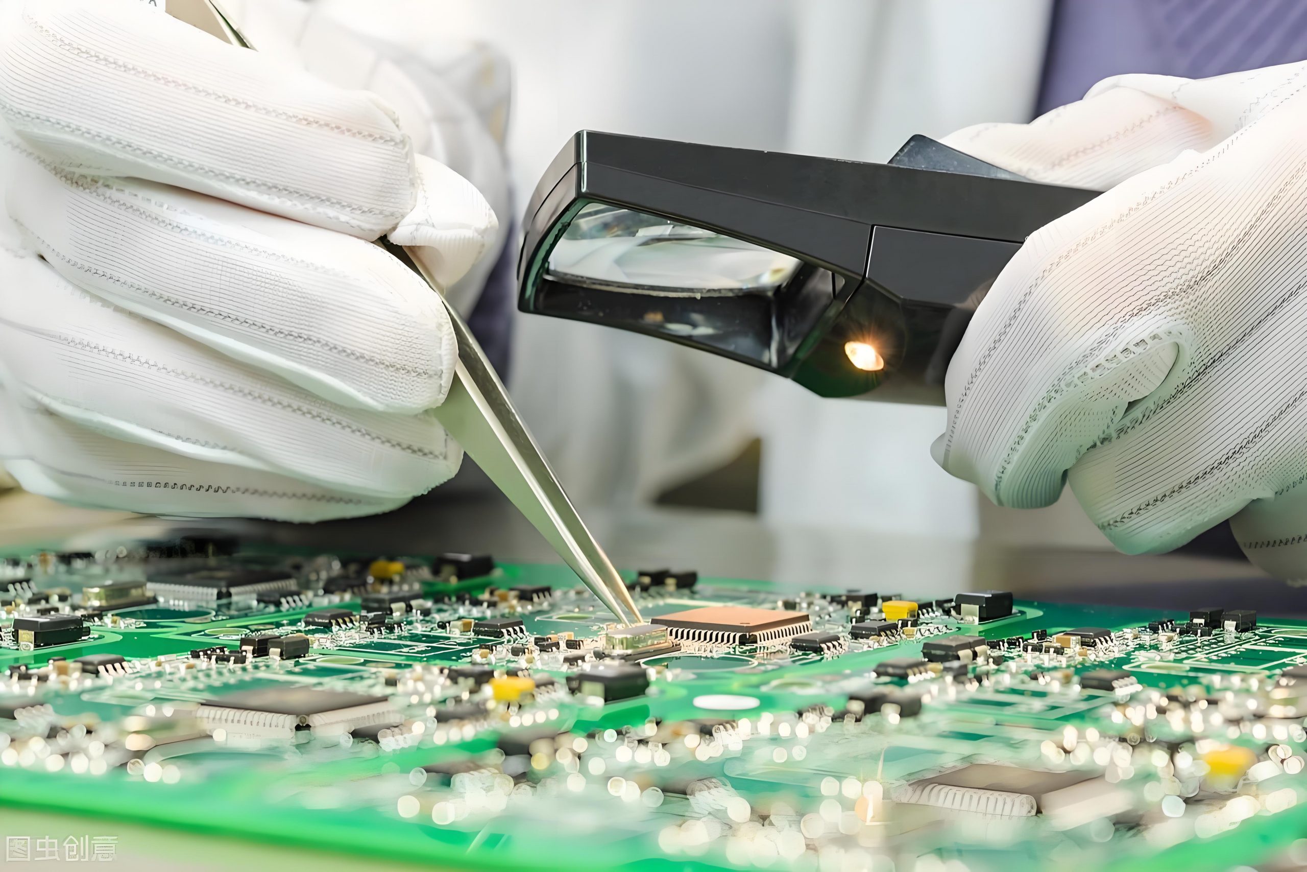
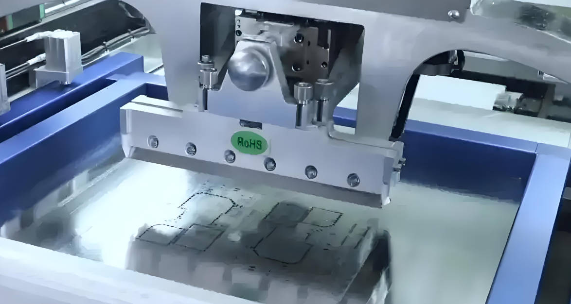
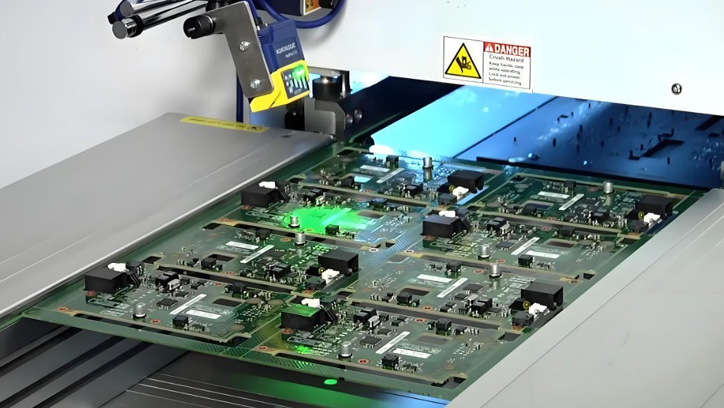
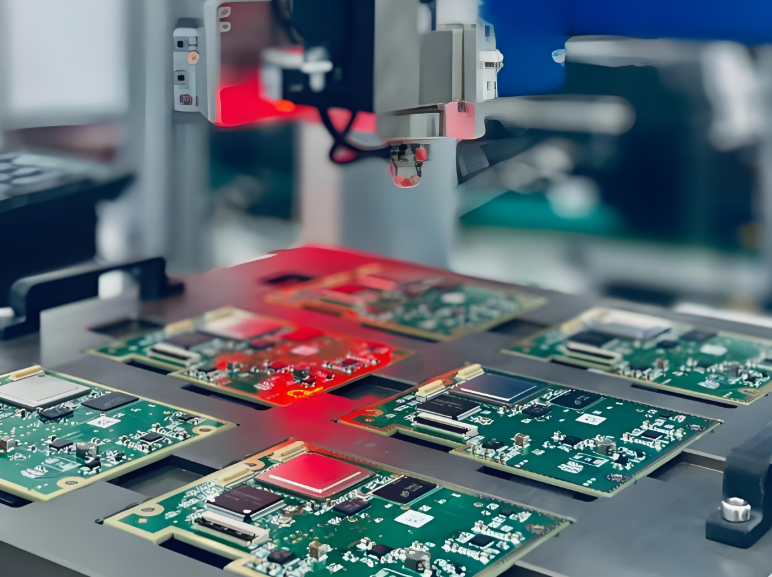
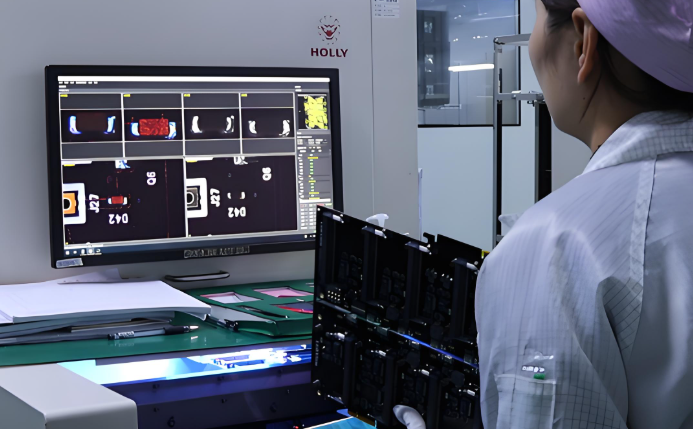
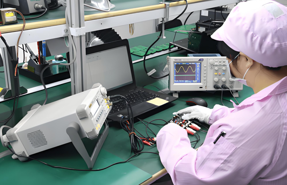
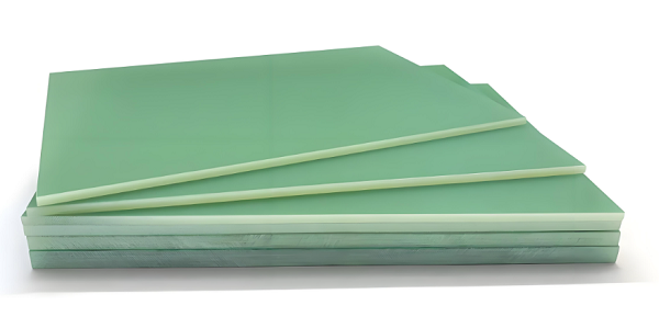
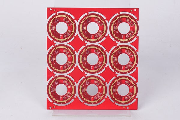
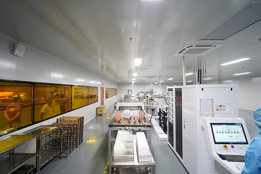
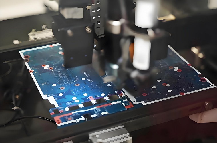
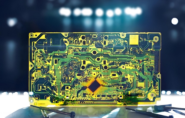
EBest Circuit (Best Technology) is a leading electronic prototype manufacturer in China specializing in all types of PCBs, from standard FR4 boards to advanced ceramic substrates. They provide quick-turn prototyping and small-batch production, focusing on high-reliability applications.
Location: Shenzhen, Guangdong, China
Services:
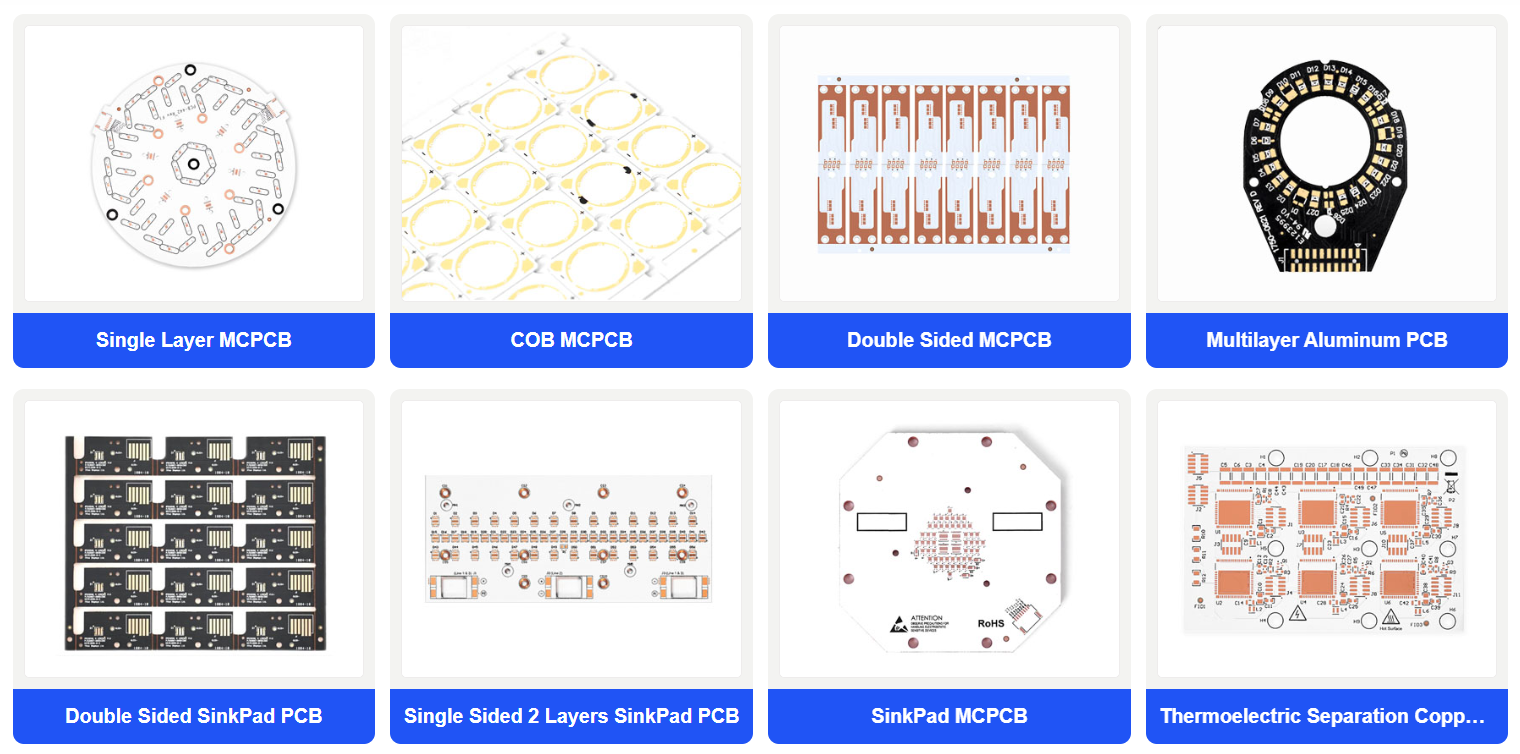
- PCB prototyping (FR4, metal core, ceramic, flex, rigid-flex)
- PCB assembly (SMT, THT, mixed assembly)
- Design support and engineering services
- One-stop EMS
Industries Served: Medical, aerospace, automotive, industrial control, LED lighting, and communication
Key Differentiators:
- In-house DFM & DFT engineering support
- MES system for full traceability
- Fast delivery (as quick as 24 hours)
- Strong ceramic PCB capability
Certifications:
ISO9001, ISO13485, IATF16949, AS9100D, UL, RoHS, REACH
2. Seeed Studio Fusion
Seeed Studio offers rapid prototyping services through its Fusion PCB platform, aimed at makers, startups, and hardware innovators globally.
Location: Shenzhen, Guangdong, China
Services:
- PCB prototyping and assembly
- CNC machining and 3D printing
- BOM sourcing
- Turnkey PCB solutions
Industries Served: IoT, robotics, consumer electronics, education, and R&D
Key Differentiators:
- Maker-friendly with global shipping
- Low-cost prototype offers
- Open-source hardware community engagement
Certifications: ISO9001, RoHS
3. JLCPCB
JLCPCB is one of the most well-known PCB prototyping companies in China, recognized for its ultra-low-cost PCB production and fast turnaround.
Location: Jiangxi and Shenzhen, China
Services:
- PCB fabrication
- PCB assembly
- SMT stencil service
- Online ordering system
Industries Served: Consumer electronics, education, prototyping labs, startups
Key Differentiators:
- Extremely low-cost PCBs (as low as $2)
- Mass production capabilities
- 24/7 customer support
Certifications: ISO9001, ISO14001, UL, RoHS
4. PCBWay
PCBWay is a trusted online PCB prototyping and assembly platform offering services from design to finished product.
Location: Shenzhen, Guangdong, China
Services:
- PCB manufacturing
- PCB assembly
- CNC, 3D printing
- Component sourcing
Industries Served: Medical devices, robotics, consumer electronics, automotive
Key Differentiators:
- Intuitive online quote system
- No minimum order quantity
- Active community and sponsorship programs
Certifications: ISO9001, UL, RoHS
5. ALLPCB
ALLPCB is a fast-growing PCB manufacturer offering ultra-fast delivery and instant quoting, ideal for prototyping and urgent projects.
Location: Hangzhou, Zhejiang, China
Services:
- PCB fabrication
- SMT assembly
- Component sourcing
- Online instant quotation
Industries Served: Automotive, LED, wearables, smart appliances
Key Differentiators:
- Express delivery (same-day shipping)
- Automated ordering system
- Multi-language customer service
Certifications: ISO9001, UL, RoHS, IATF16949
6. Hitech Circuits Co., Ltd.
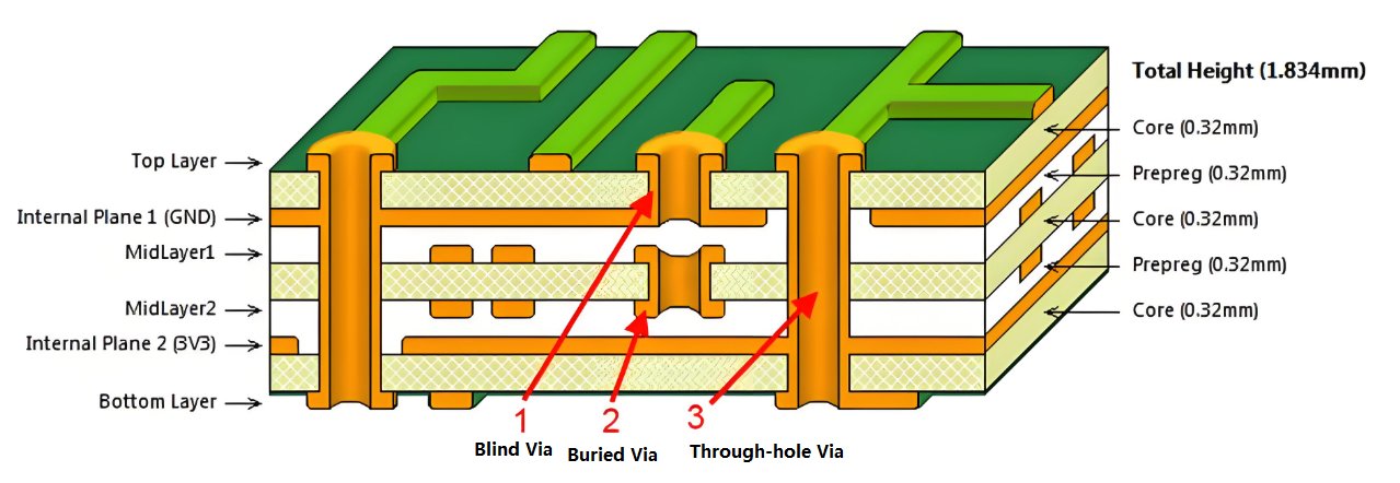
Hitech Circuits is a professional PCB manufacturer with a focus on quick-turn prototypes and HDI PCB solutions.
Location: Shenzhen, Guangdong, China
Services:
- Quick-turn PCB manufacturing
- HDI PCB and multilayer boards
- PCB assembly
- DFM/DFT support
Industries Served: Industrial control, telecom, defense, medical
Key Differentiators:
- High-end PCB capabilities (HDI, via-in-pad)
- Fast delivery and engineering expertise
- IPC Class 3 production
Certifications: ISO9001, ISO13485, IATF16949, UL
7. Sunthone Electronics
Sunthone offers low-to-medium volume PCB manufacturing and assembly with a strong focus on cost-effective prototyping.
Location: Shenzhen, Guangdong, China
Services:
- PCB production
- PCB assembly
- PCB design and layout services
- Turnkey solutions
Industries Served: Smart home, wearable tech, industrial automation
Key Differentiators:
- Competitive pricing for small runs
- Component procurement support
- Quick prototype turnaround
Certifications: ISO9001, UL, RoHS, IPC
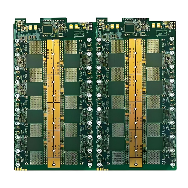
8. Shenzhen Kinwong Electronic Co., Ltd.
Kinwong is one of China’s top 100 PCB manufacturers, offering full-range PCB solutions with strong R&D capabilities.
Location: Shenzhen, Guangdong, China
Services:
- Rigid PCB
- FPC and rigid-flex
- HDI and multilayer PCB
- Engineering support
Industries Served: Automotive, mobile, telecom, medical electronics
Key Differentiators:
- Large-scale manufacturing
- Independent R&D team
- Trusted by global Tier 1 customers
Certifications: ISO9001, ISO14001, IATF16949, AS9100D, UL
9. A-TECH Circuits Co., Ltd.
A-TECH specializes in precision PCB manufacturing for time-critical and advanced PCB prototypes.
Location: Shenzhen, Guangdong, China
Services:
- Single to 20-layer PCB
- High-frequency boards
- Impedance control
- PCB prototypes
Industries Served: RF communications, power electronics, medical, aerospace
Key Differentiators:
- Strong in RF/high-speed boards
- Customized engineering service
- On-time delivery for prototypes
Certifications: ISO9001, UL, RoHS, TS16949
10. Weller Technology Co., Ltd.
Weller Technology is an advanced PCB and PCBA manufacturer focused on rapid prototyping and precision assembly.
Location: Dongguan, Guangdong, China
Services:
- PCB prototyping
- High-precision SMT and THT
- Rigid-flex and FPC manufacturing
- Component sourcing
Industries Served: Medical devices, avionics, automotive, consumer electronics
Key Differentiators:
- Strong R&D for special boards
- Cleanroom-level SMT assembly
- Fast cycle prototyping
Certifications: ISO13485, ISO9001, IATF16949, UL
FAQs
1. Why choose a Chinese manufacturer for electronic prototypes?
Chinese manufacturers offer a unique combination of speed, cost-effectiveness, and advanced production capabilities. Many companies also support low-volume orders and rapid prototyping, making them ideal for startups and engineers in the R&D phase.
2. How fast can Chinese companies deliver PCB prototypes?
Lead times vary by company and complexity, but some manufacturers like EBest Circuit (Best Technology) or ALLPCB can deliver simple prototypes within 24 to 72 hours.
3. What is the minimum order quantity (MOQ) for PCB prototyping in China?
Most Chinese PCB manufacturers support very low or even zero MOQs for prototype runs. Services like PCBWay and JLCPCB are known for allowing single-piece orders.
4. How can I ensure quality when working with a Chinese manufacturer?
Check the manufacturer’s certifications (like ISO9001, IATF16949, or UL), ask for real case studies or test reports, and verify their traceability systems. Working with experienced companies like EBest Circuit (Best Technology) also reduces risk.
5. Can these companies help with component sourcing and assembly?
Yes. Many Chinese electronic prototype manufacturers offer turnkey solutions including PCB fabrication, component sourcing, SMT assembly, and testing—all under one roof.