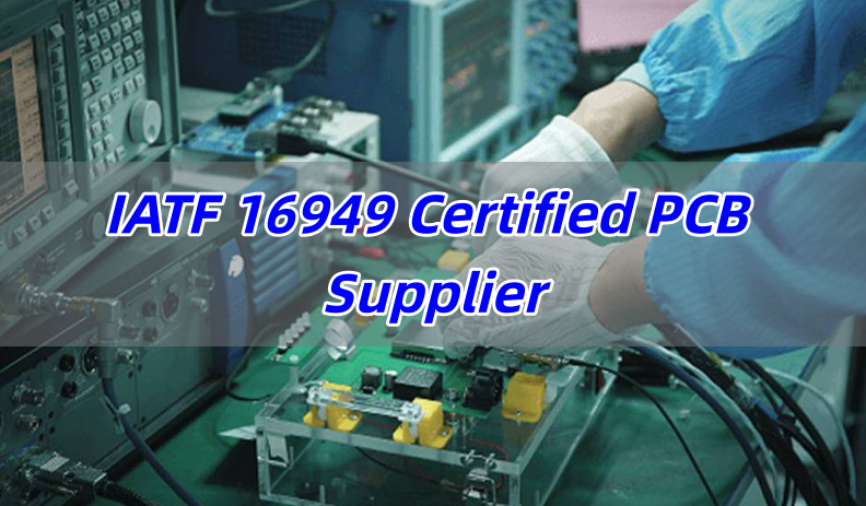
Selecting an IATF 16949 certified PCB supplier is not just a purchasing decision—it is a risk management strategy for automotive electronics. With vehicles increasingly dependent on electronics for safety, performance, and connectivity, PCB quality directly impacts system reliability and brand reputation.
This in-depth guide explains what IATF 16949 certification means for PCB manufacturing, how it affects automotive applications, how to evaluate certified suppliers, and why EBest Circuit (Best Technology) is a trusted partner for automotive PCB projects.
What Is an IATF 16949 Certified PCB?
An IATF 16949 certified PCB is a printed circuit board manufactured under a quality management system that complies with IATF 16949, the global automotive industry standard that replaced ISO/TS 16949.
Unlike general ISO 9001 certification, IATF 16949 is automotive-specific and focuses on:
- Defect prevention rather than detection
- Risk-based process control
- Continuous improvement throughout the supply chain
- Traceability and accountability at every manufacturing stage
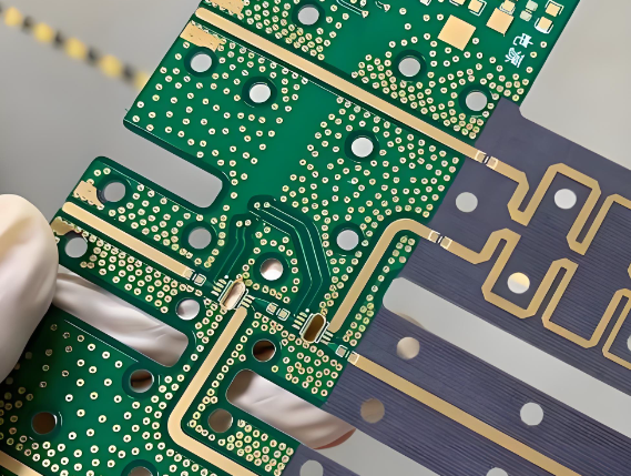
For PCB manufacturing, this means every process—from laminate sourcing and copper plating to imaging, drilling, surface finish, and final inspection—is documented, controlled, audited, and continuously improved.
An IATF 16949 certified PCB supplier is qualified to support automotive OEMs, Tier 1 suppliers, and Tier 2 suppliers globally.
Typical Applications for IATF 16949 Certified PCBs
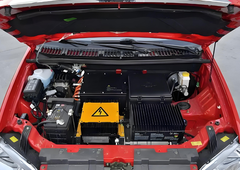
Automotive electronics operate in environments that are far more demanding than consumer or industrial electronics. As a result, IATF 16949 certified PCBs are widely used in systems where failure is unacceptable, like:
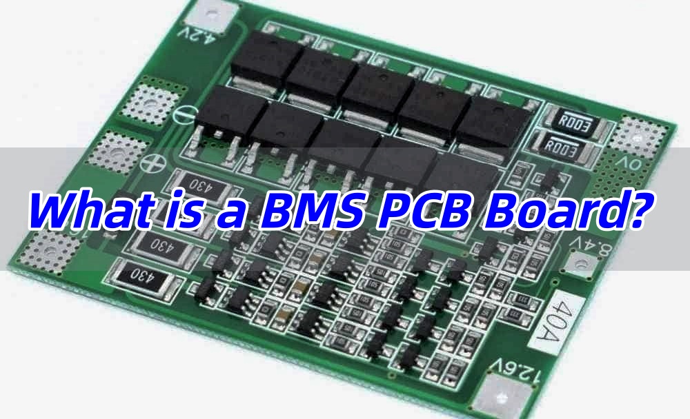
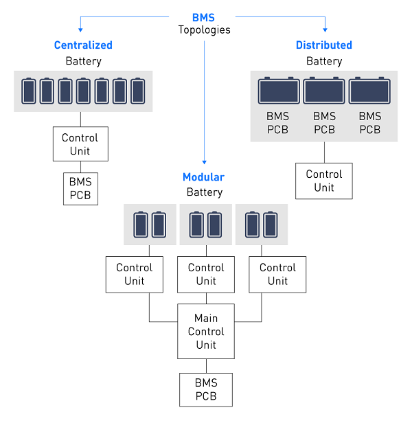
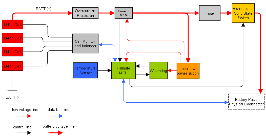
- Electric vehicle (EV) systems – BMS, OBC, inverters, DC-DC converters
- ADAS & autonomous driving modules – radar, camera, LiDAR control boards
- Powertrain & engine control units (ECU)
- Infotainment and cockpit electronics
- Body electronics – lighting control, window and seat modules
- Chassis and safety systems – ABS, EPS, airbag controllers
These applications demand high reliability, thermal stability, and long service life, often exceeding 10–15 years.
Why IATF 16949 Certification Is Critical in Automotive Electronics?
Automotive PCBs must survive:
- Temperature ranges from -40°C to +125°C or higher
- Continuous vibration and mechanical shock
- Long-term exposure to humidity, oils, and chemicals
- 10–20 years of operational life
IATF 16949 certification ensures that a PCB supplier has systems in place to manage these risks through:
- APQP (Advanced Product Quality Planning) for new product introduction
- FMEA (Failure Mode and Effects Analysis) to identify and mitigate risks
- SPC (Statistical Process Control) to maintain consistency
- Root cause analysis and corrective actions (8D, PDCA)
- Supplier quality management for raw materials
Without IATF 16949, PCB quality may rely too heavily on final inspection rather than process stability, which is unacceptable for automotive use.
Does IATF 16949 Mean Zero Defects?
No quality standard can guarantee absolute zero defects—but IATF 16949 is designed to make defects rare, predictable, and preventable. Instead of reacting to failures, IATF 16949 requires:
- Early risk identification
- Process capability monitoring
- Immediate corrective action when trends appear
- Continuous reduction of variation
In practice, this leads to dramatically lower defect rates, improved field reliability, and reduced recall risk for automotive customers.
Does IATF Certification Automatically Mean Automotive Capability?
No, not always. IATF 16949 certifies the quality management system, not the technical capability alone.
A truly automotive-capable IATF 16949 certified PCB supplier must also demonstrate:
- Experience with automotive-grade laminates (high Tg, low CTE, CAF-resistant)
- Tight control of dielectric thickness and impedance
- Stable copper plating and via reliability
- High-reliability surface finishes (ENIG, ENEPIG, Immersion Silver)
- Proven performance in thermal cycling and reliability testing
Certification plus real automotive project experience is the key.
What Makes an IATF 16949 Certified PCB Manufacturer Different?
Compared to standard PCB manufacturers, IATF 16949 certified suppliers offer:
- Full lot and serial traceability
- Controlled change management (ECN & PCN)
- PPAP documentation upon request
- Automotive-focused process audits
- Long-term supply consistency
These differences are essential for OEMs who cannot afford field failures or recalls.
How to Verify an IATF 16949 Certified PCB Supplier?
Before selecting a supplier, always verify:
- Valid IATF 16949 certificate (issued by an accredited certification body)
- Certificate scope explicitly covering PCB manufacturing
- Evidence of automotive project experience
- Ability to provide PPAP, FMEA, control plans, and traceability records
- Clear change management and corrective action procedures
A professional IATF 16949 certified PCB supplier will proactively provide this information.
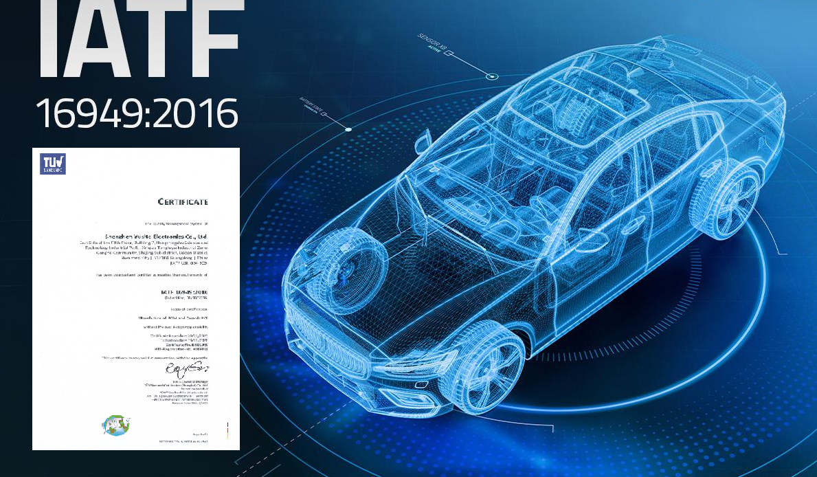
EBest Circuit (Best Technology) – Your Reliable IATF 16949 Certified PCB Supplier
EBest Circuit (Best Technology) is a trusted IATF 16949 certified PCB supplier, supporting automotive electronics manufacturers with stable quality, engineering expertise, and long-term production reliability.
At EBest Circuit (Best Technology), our automotive PCBs are manufactured under a fully implemented IATF 16949 quality management system, ensuring process stability, traceability, and long-term reliability for safety-critical automotive electronics.
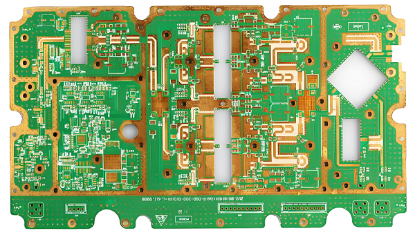
Our Automotive PCB Manufacturing Capability
| Category | Capability Details |
| Certification | IATF 16949 (Automotive Quality Management System) |
| PCB Types | Single-sided, Double-sided, Multilayer Automotive PCBs |
| Layer Count | 1–20+ layers (automotive control & power applications) |
| Base Materials | FR-4 (High Tg), Low-loss laminates, Automotive-grade materials |
| Tg Range | ≥170°C (automotive and high-reliability requirements) |
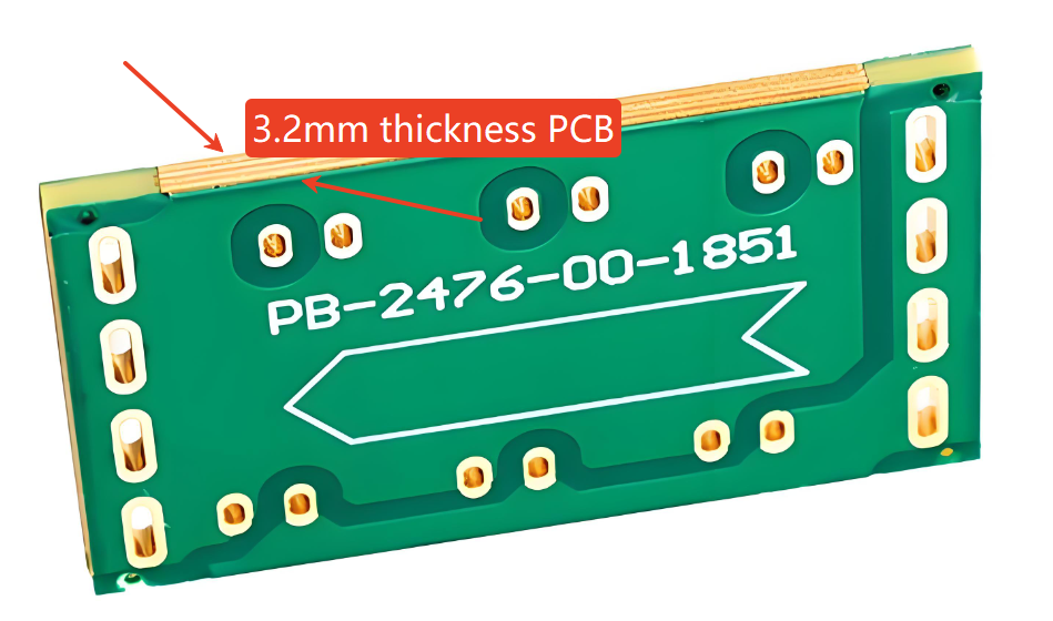
| Board Thickness | 0.4 mm – 3.2 mm (custom thickness available) |
| Copper Thickness | 0.5 oz – 6 oz (inner & outer layers) |
| Heavy Copper PCB | Up to 6 oz for EV power electronics |
| Min Line / Space | 4 / 4 mil (HDI options available) |
| Min Hole Size | 0.20 mm (laser vias for HDI upon request) |
| Aspect Ratio | Up to 10:1 |
| Impedance Control | ±5% tolerance (automotive signal integrity requirements) |
| Surface Finishes | ENIG, ENEPIG, Immersion Silver, Immersion Tin, OSP |
| Solder Mask | Automotive-grade epoxy, green / black / red (others on request) |
| Silkscreen | White, yellow (high contrast for traceability) |
| Panel Size | Up to 600 × 1200 mm |
| CAF Resistance | CAF-resistant material selection & process control |
| Thermal Reliability | Designed for −40°C to +125°C operating environments |
| Electrical Testing | Flying Probe Test, Fixture E-Test (100% testing) |
| Inspection | AOI, X-ray (for HDI & fine-pitch designs) |
| Reliability Testing | Thermal shock, thermal cycling (upon request) |
| Traceability | Full lot & material traceability per IATF 16949 |
| Documentation Support | PPAP, Control Plan, PFMEA, SPC records |
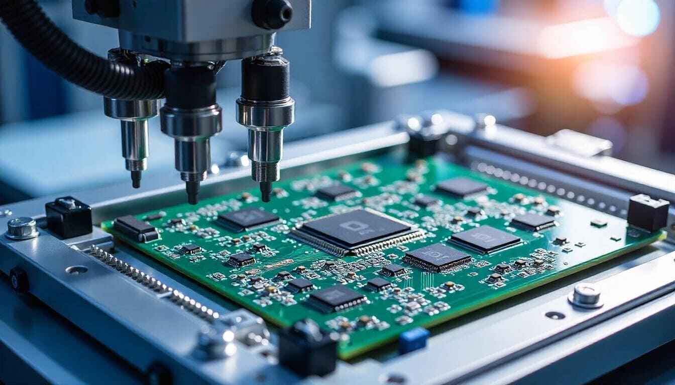
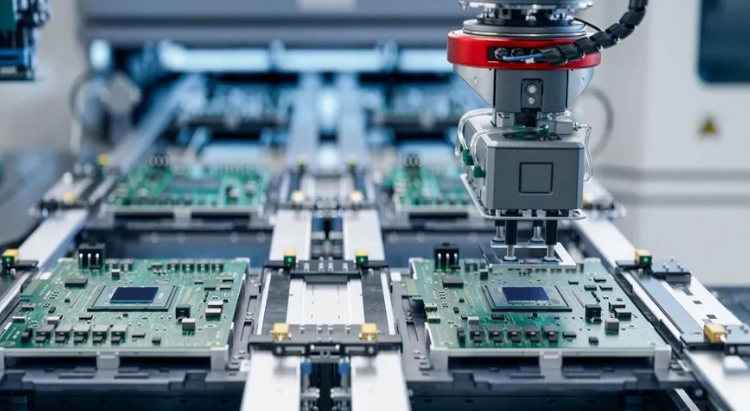
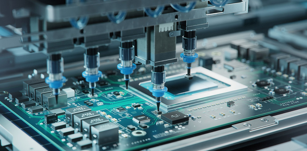
Our Services for IATF 16949 Certified PCB Projects
We provide comprehensive support throughout the product lifecycle:
- Automotive PCB DFM and engineering review
- Prototype, NPI, and mass production support
- PPAP and quality documentation assistance
- Long-term supply and lifecycle management
- PCB & PCBA one-stop manufacturing solutions
Our goal is to help customers reduce risk, shorten development cycles, and scale confidently. If you’re searching for a dependable iatf 16949 certified pcb supplier, EBest Circuit (Best Technology) is ready to support your automotive electronics projects.
Frequently Asked Questions (FAQ)
1. Is IATF 16949 mandatory for automotive PCBs?
Most automotive OEMs and Tier 1 suppliers require IATF 16949 certification for PCB suppliers.
2. Can IATF 16949 certified suppliers support EV and ADAS projects?
Yes. IATF 16949 is widely adopted in EV, hybrid, and autonomous vehicle electronics.
3. Does IATF 16949 cover PCB assembly?
Only if PCBA is included in the certification scope. Always verify the certificate details.
4. How often is IATF 16949 audited?
Certified suppliers undergo annual surveillance audits and full recertification every three years.