You know, bendable aluminum PCBs have gained prominence in various electronic applications due to their unique ability to flex and conform to curved surfaces. Unlike traditional rigid PCBs that are commonly composed of materials like fiberglass , these PCBs utilize aluminum as the base material, allowing it bendable and flexibility when needed. Compared to the rigid characteristics of traditional metal core PCB, bending aluminum PCB can be adapted to specific space requirements and shape requirements. In this article, we will introduce the characteristics of bendable aluminum PCBs and explore the key considerations that engineers and manufacturers need to pay attention during the design and production process.
What Are the Benefits of Bendable Aluminum PCBs?
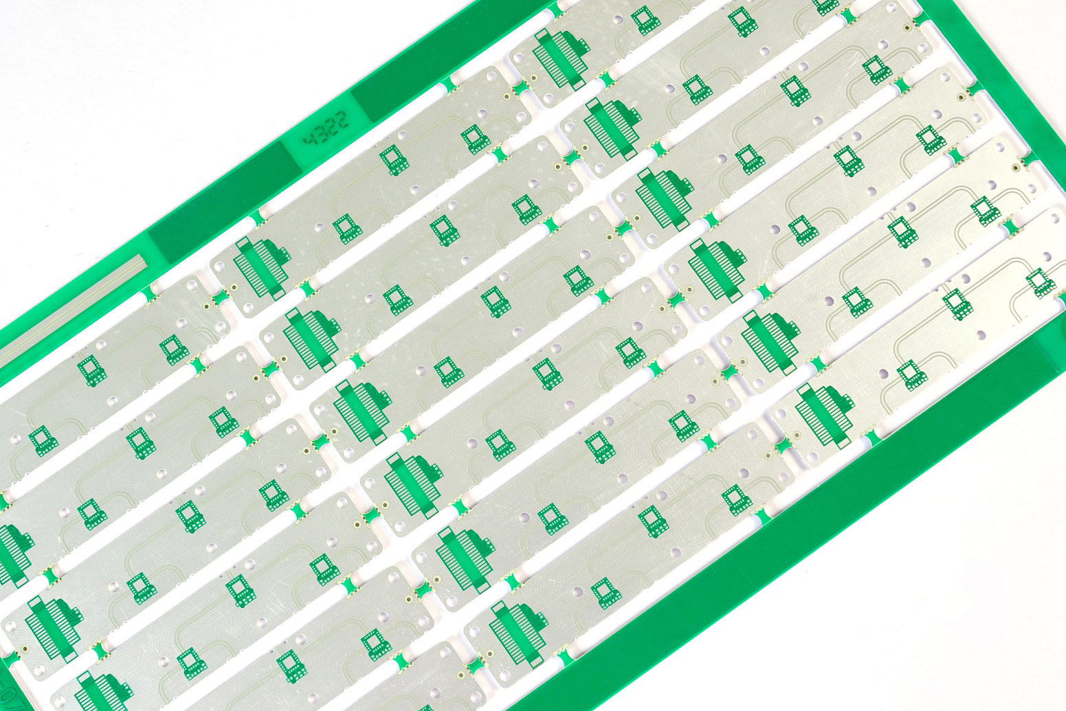
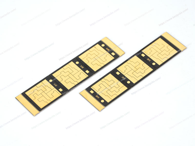
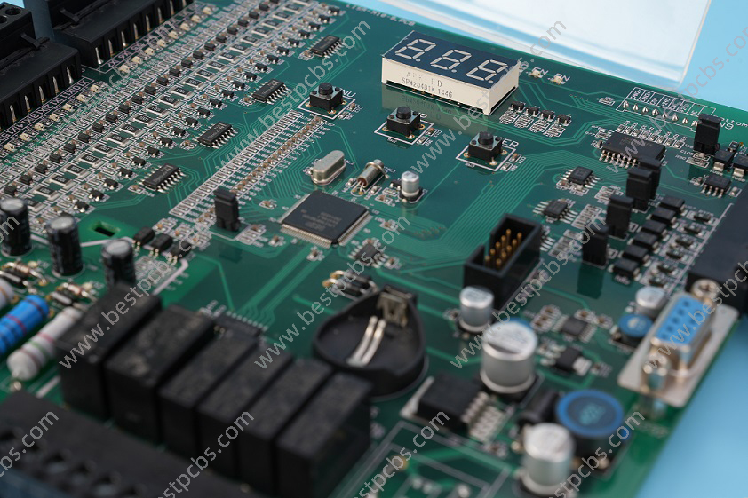
May some designers are reraly to know the bendable aluminum PCB, in their congnition, the bendable PCBs are including flex circuits, rigid flexible circuit and FFC, and aluminum PCB is classfied into one of rigid PCB. But here, EBest Circuit (Best Technology) is so proud to say, we have developed bendable aluminum PCB and we can manufacture it with fast delivery and high-quality, this is what we prouded.
The primary advantage of bendable aluminum PCBs is their flexibility. They can be bent and shaped to fit into various form factors and designs, making them suitable for applications where space is limited or where flexibility is required and traditional rigid boards are not ideal. Common applications include wearable devices, curved displays, and other electronic systems with unconventional form factors.
Additionally, bendable aluminum PCB has the advantages of aluminum, so it has good heat dissipation and higher thermal management than traditional PCBs. This feature is crucial for maintaining the reliability and performance of electronic devices, especially those operating in high-temperature environments.
Considerations During the Design Process
Al Material Selection:
Considering that it is a bendable aluminum substrate, it must be satisfied that the material selection should be bendable but at the same time have good heat dissipation of the metal base. This aluminum base material is a specially designed aluminum alloy or aluminum base composite material. Meanwhile, the thickness of the material is critical, such as the material is generally from 0.2mm to 1.6mm, of which 0.2mm to 1.0mm is the more common bending metal substrate thickness.
Flexibility Requirements:
Defining the flexibility requirements is a crucial step in the design process. The degree of bending, bending radius, and any other factors related to flexibility must be clearly defined based on the intended application. For instance, a wearable fitness tracker might require a specific bending profile to comfortably conform to the curvature of the wrist.
Also note that the bending radius is different for materials of different thicknesses. In general, a smaller bending radius usually corresponds to a thinner board material, while a larger bending radius can accommodate a thicker board material.
Circuit Layout:
The layout of the circuit components plays a pivotal role in ensuring the longevity of bendable aluminum PCBs. Designers should strategically plan the arrangement of components to accommodate bending without subjecting critical elements, such as sensors or microcontrollers, to excessive stress. Even distribution of components contributes to a balanced bending profile.
And the pad should not be designed at the bend of the bending, which will cause damage to the assembly components after bending, or even no way to bend. In addition, the welding pad near the bending cross should also be kept away from the bending line to avoid collision and extrusion of the components after bending.
Bending Radius:
Determining the minimum bending radius that the PCB can tolerate is essential for preventing structural damage or compromise in electrical performance. Specific bending radii should be defined based on the application’s needs. For example, a bendable aluminum PCB designed for a wearable device might need to withstand repeated bending with a predefined radius.
Dielectric Layer:
Choosing an appropriate dielectric material is crucial for maintaining insulation between different layers of the PCB. The dielectric layer should possess flexibility to withstand bending without compromising its insulating properties.
As we know, when design the aluminum PCB, the thermal conductivity is also important. Bendable aluminum also has the thermal conductivity requirement, but when the thermal conductivity material is higher, the higher the content of ceramic powder in material. And when the content of ceramic powder is higher, the brittleness of the material is higher, and it is easier to break or break after bending. The material of 1W/m.k is more bendable than 3W/m.k。

Considerations During the Manufacturing Process
Bendable aera line:
For the production requirements of the light plate, the V-cut mark is generally used to determine the complete line at the bend, and attention should be paid to the depth control of the v-cut, so as not to damage the line.
Testing and Validation:
Prototyping is a vital phase in the manufacturing process of bendable aluminum PCBs. Thorough testing and validation are necessary to ensure that the PCB meets the required electrical and mechanical specifications. Bending tests simulating the intended application conditions should be performed to assess the PCB’s durability. such as bending test, bending angle test.
Generally speaking, after the bare board finished, it’s not bendable to the required angle. In order to avoid bad transportation or collision, some customers require not to bend and they will bend it by themselves. But if the customers don’t want to bend the board by himself, we also can help to bend it, it will require mold and it need to custom the package for shipping. The custom package can help to protect the damage in shipping.
Collaboration with Manufacturers:
Close collaboration with experienced PCB manufacturers is key to successful production. Manufacturers with expertise in flexible PCB fabrication can provide valuable insights into the manufacturing process. Working together ensures that the design aligns with manufacturing capabilities, optimizing the production of bendable aluminum PCBs.
Conclusion
In a word, the design and manufacturing of bendable aluminum PCBs involve a series of critical considerations to ensure the success and reliability of the final product. From material selection and flexibility requirements to testing, validation, and compliance with industry standards, each step plays a pivotal role in creating PCBs that meet the unique demands of modern electronic applications. By carefully addressing these considerations, designers and manufacturers can unlock the full potential of bendable aluminum PCBs in diverse and innovative electronic devices. Welcome to contact EBest Circuit (Best Technology) if you want to know more.