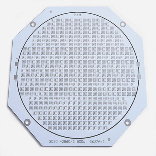
Why Choose EBest for Your LED Street Light Aluminum PCB?
When sourcing LED Street Light Aluminum PCB, EBest is your most reliable partner—offering industry-leading specs, consistent performance, and hassle-free service. Our core goal is to deliver boards that enhance your street light’s durability and efficiency, backed by 19+ years of PCB expertise.
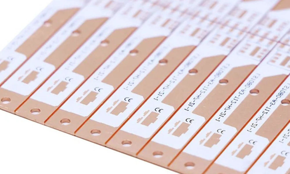
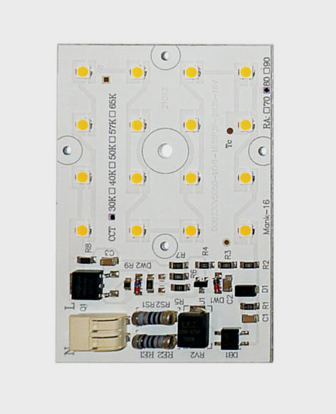
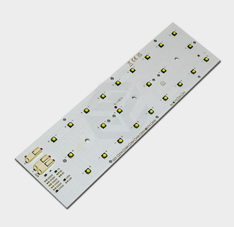
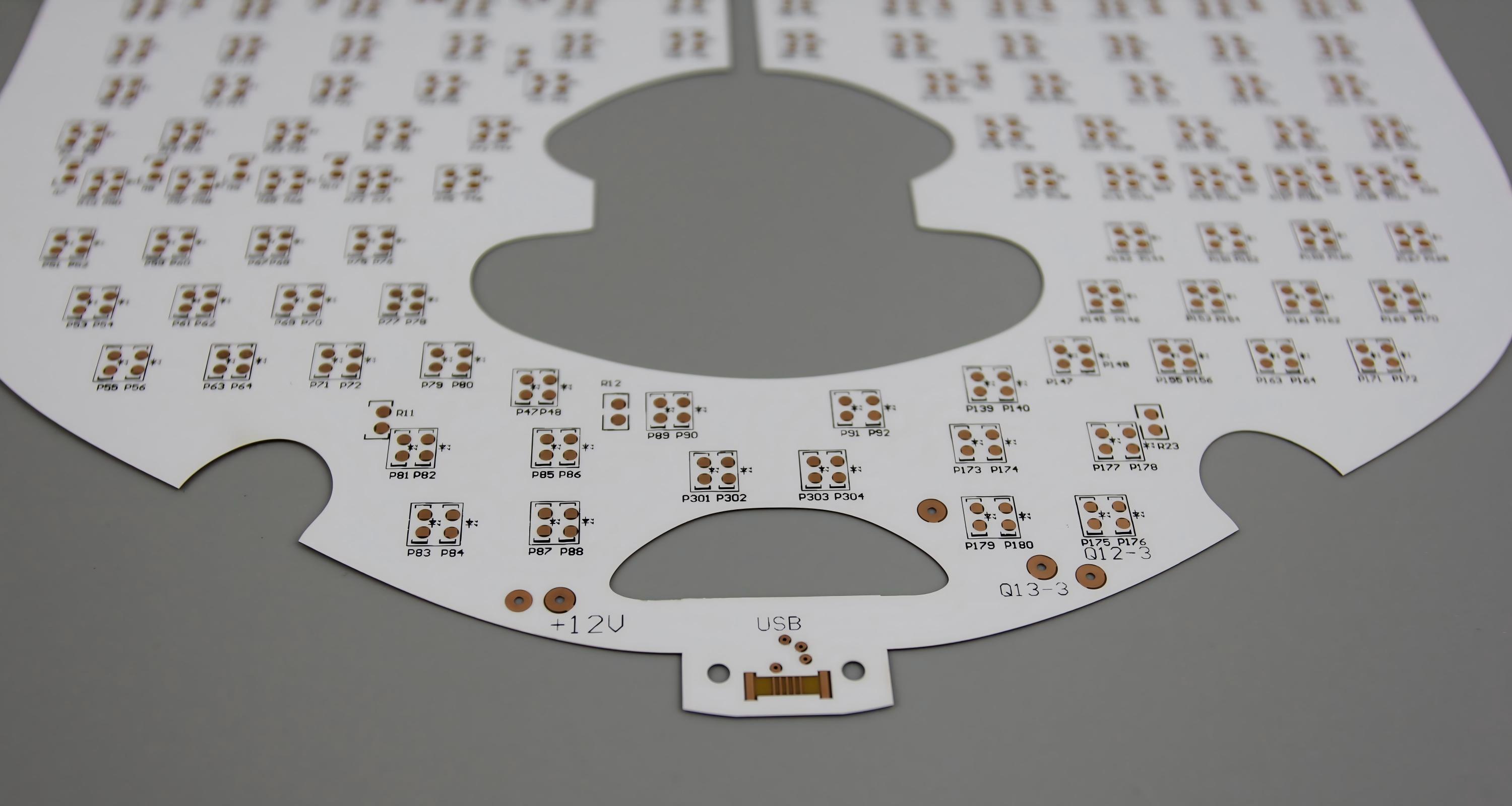
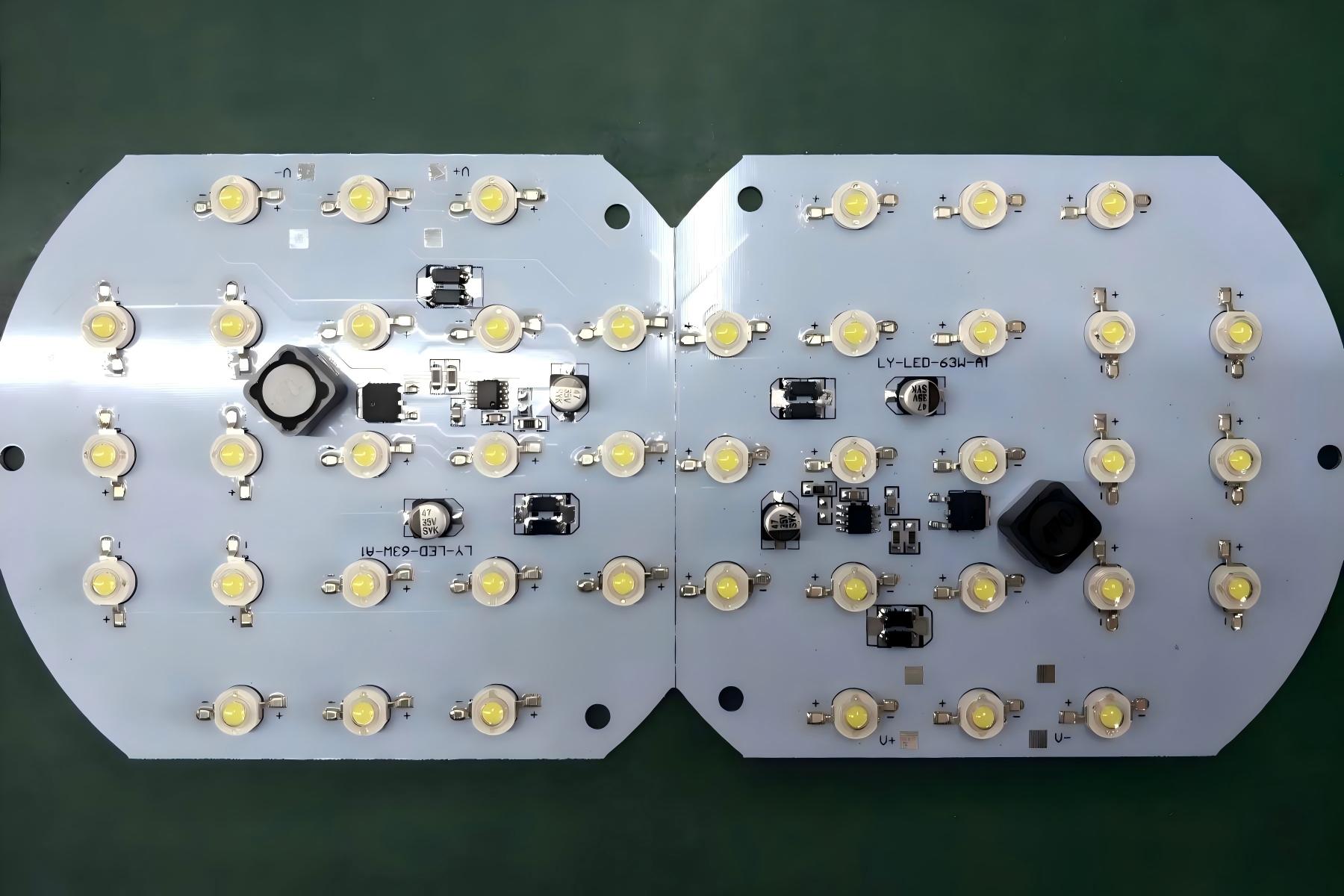
Our LED Street Light Aluminum PCB core parameters meet and exceed industry standards: Thermal conductivity ranges from 1–5 W/m·K, aluminum base thickness 1.0–3.0mm (customizable), copper weight 1–3 oz, dielectric thickness 50–150μm, and operating temperature range -40℃ to 85℃. All boards are designed for outdoor durability, corrosion resistance, and optimal heat dissipation.
Stop settling for subpar PCBs that risk premature street light failure. Choose EBest for your LED Street Light Aluminum PCB needs—contact us today to place your order and experience unmatched quality and service.
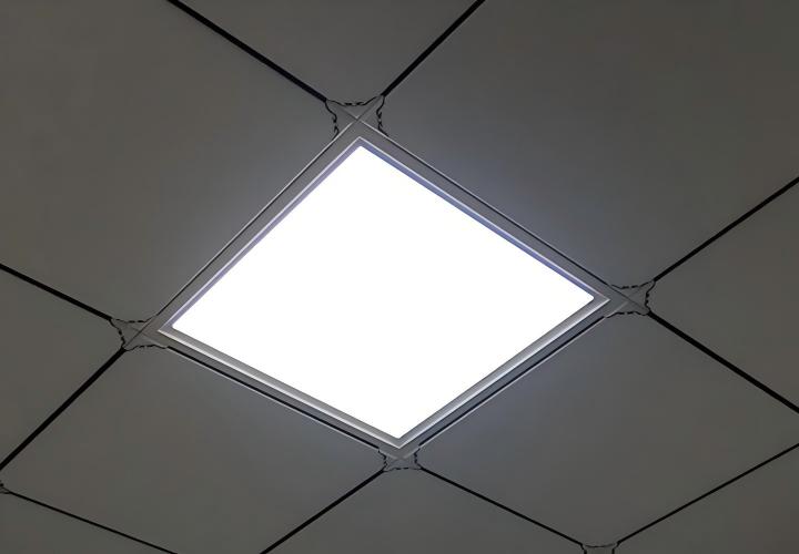
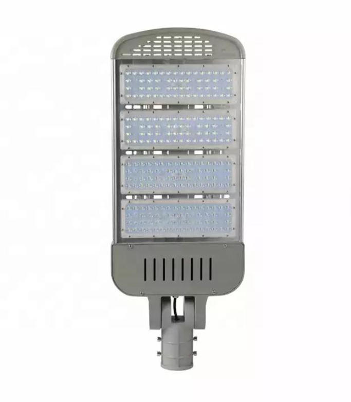
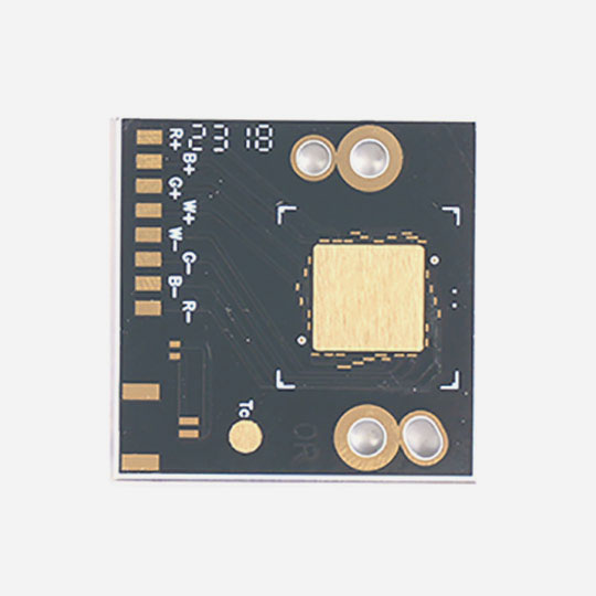
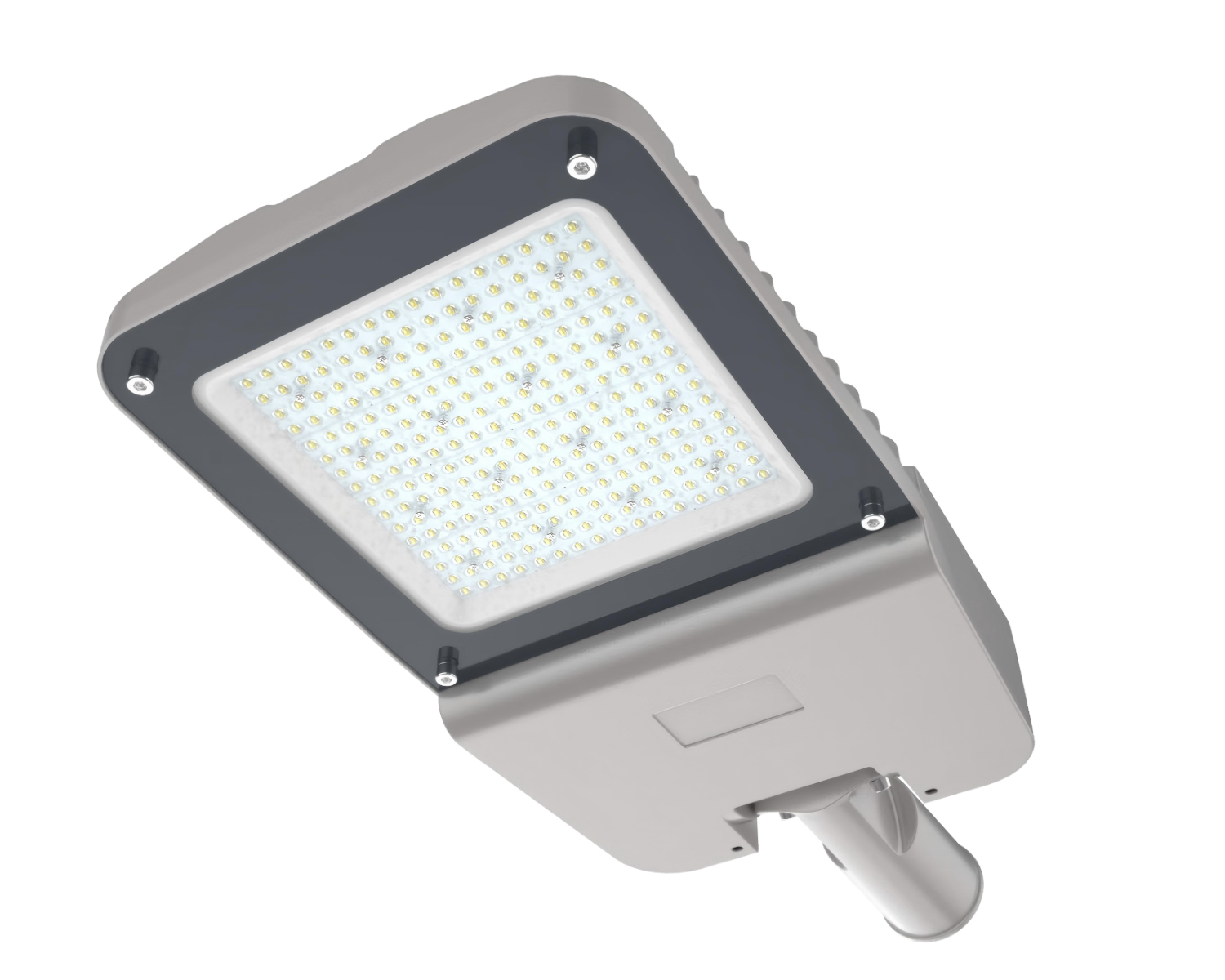
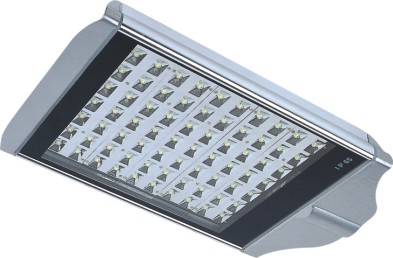
What Is an LED Street Light Aluminum PCB, and Why Is It Essential for Outdoor Lighting?
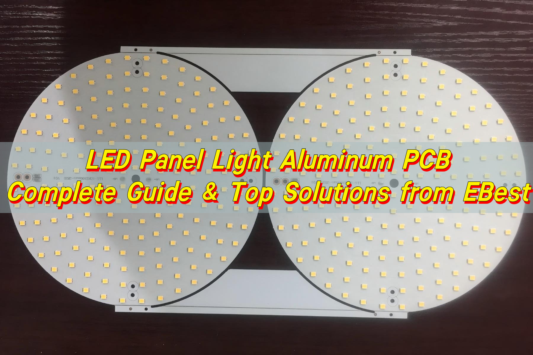
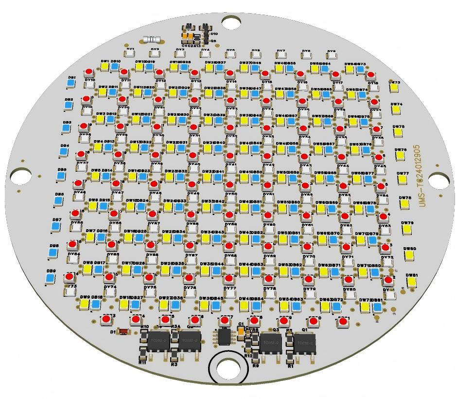
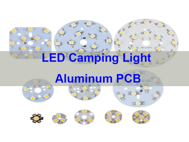
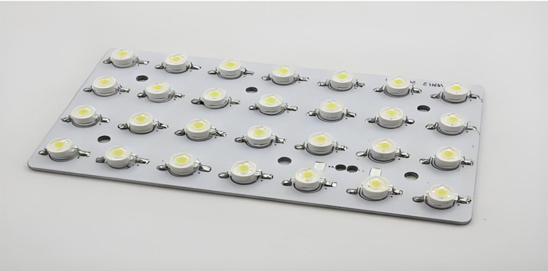
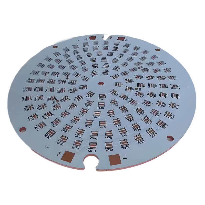
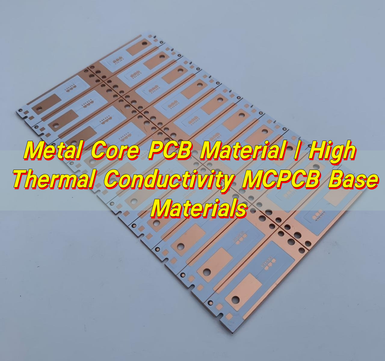
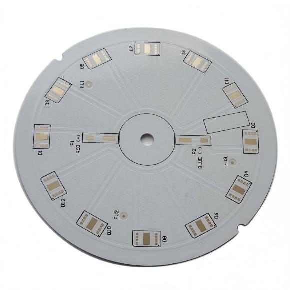
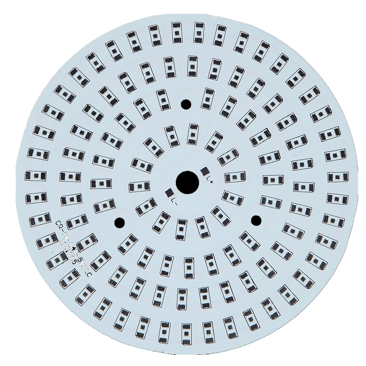
An LED Street Light Aluminum PCB is a metal core PCB (MCPCB) that uses aluminum as its base material, designed specifically to address the heat management challenges of outdoor LED street lights. It features a three-layer structure: circuit layer, thermally conductive dielectric layer, and aluminum base.
LEDs convert 60–80% of input power into heat, and poor heat dissipation shortens their lifespan by 50% for every 10℃ rise above 85℃. LED Street Light Aluminum PCB solves this by acting as an integrated heat sink, reducing thermal resistance to 1–2℃ per watt—10–20x better than standard FR4 boards.
Without a high-quality LED Street Light Aluminum PCB, street lights suffer from lumen depreciation, color shifting, and premature failure, increasing maintenance costs and reducing safety for outdoor areas.
How Does LED Street Light Aluminum PCB Improve Thermal Management for Outdoor Use?
LED Street Light Aluminum PCB improves thermal management through its specialized structure and material properties, ensuring street lights perform reliably in harsh outdoor conditions.
Key Thermal Management Features
- Aluminum base (typically 1050, 1060, 5052, or 6061 alloy) with thermal conductivity 138–234 W/m·K, efficiently spreading heat across the board surface.
- Thermally conductive dielectric layer (1.0–3.0 W/m·K) that transfers heat from the circuit layer to the aluminum base without compromising insulation.
- Optimized copper traces and thermal vias (8–12 per cm²) to direct heat away from LED chips, keeping junction temperatures below 85℃.
This design ensures LED Street Light Aluminum PCB maintains stable performance in extreme temperatures, from -40℃ cold to 85℃ heat, critical for outdoor street lighting durability.
What Are the Top Applications of LED Street Light Aluminum PCB? 4 Industry Case Studies
LED Street Light Aluminum PCB is widely used across outdoor lighting and related industries, with proven performance in diverse scenarios. Below are four popular industry case studies showcasing our solutions.
Case Study 1: Municipal Street LightingA municipal government needed durable LED Street Light Aluminum PCB for 5,000+ street lights across urban and rural areas. We delivered boards with 1.6mm aluminum base, 2oz copper, and 100μm dielectric layer.
Result: 3-year service life with only 12% light decay, 40% less maintenance than previous FR4-based street lights, and stable performance in heavy rain and extreme temperatures.
Case Study 2: Highway Tunnel LightingA transportation company required LED Street Light Aluminum PCB for tunnel lighting, where high humidity and constant operation demand exceptional reliability. Our boards featured corrosion-resistant aluminum and waterproof dielectric layers.
Result: 24/7 operation for 2 years with zero failures, heat dissipation improved by 35%, and compliance with highway safety lighting standards.
Case Study 3: Residential Community LightingA real estate developer needed cost-effective LED Street Light Aluminum PCB for residential streets and walkways. We customized boards with 1.0mm aluminum base and optimized circuit layout to balance performance and practicality.
Result: 50,000+ hours of service life, 25% energy savings compared to traditional lighting, and seamless integration with smart lighting controls.
Case Study 4: Industrial Park LightingAn industrial park required LED Street Light Aluminum PCB for high-power street lights (50–100W) in areas with heavy machinery and dust. Our boards included thickened copper traces and anti-dust surface finishes.
Result: Stable performance in dusty environments, 15% lower operating temperature, and compatibility with industrial-grade power supplies.
How Does LED Street Light Aluminum PCB Compare to FR4 and Copper Core PCBs?
Choosing the right PCB material is critical for LED street lights. Below is a detailed comparison of LED Street Light Aluminum PCB with FR4 and copper core PCBs, highlighting key differences.
| Feature | LED Street Light Aluminum PCB | FR4 PCB | Copper Core PCB |
|---|---|---|---|
| Thermal Conductivity (W/m·K) | 138–234 (aluminum base) + 1.0–3.0 (dielectric) | 0.2–0.3 | 300–400 |
| Thermal Resistance (℃/W) | 1–2 | 20–22 | 0.5–1 |
| Outdoor Durability | High (corrosion-resistant, temperature-stable) | Low (prone to moisture damage) | High (but prone to oxidation) |
| Design Flexibility | High (single/double/multilayer options) | High (but poor heat management) | Low (complex manufacturing) |
| Suitability for LED Street Lights | Ideal (balances performance and practicality) | Not recommended (poor heat dissipation) | Overkill (unnecessary for most street light applications) |
What Are the Common Pain Points with LED Street Light Aluminum PCB?
Many users face recurring issues with LED Street Light Aluminum PCB, from poor heat dissipation to unstable supply and inconsistent quality. EBest addresses these pain points with proven solutions, ensuring your projects run smoothly.
Pain Point 1: Premature Failure Due to Poor Heat DissipationSolution: Our LED Street Light Aluminum PCB uses high-grade aluminum alloys and optimized dielectric layers, reducing thermal resistance to 1–2℃/W. We also add thermal vias and thick copper traces to eliminate hotspots, extending LED lifespan by 50%.
Pain Point 2: Inconsistent Quality Across BatchesSolution: Every LED Street Light Aluminum PCB undergoes 100% full inspection before delivery, including thermal resistance testing, insulation resistance testing, and visual inspection. Our strict quality control ensures batch-to-batch consistency.
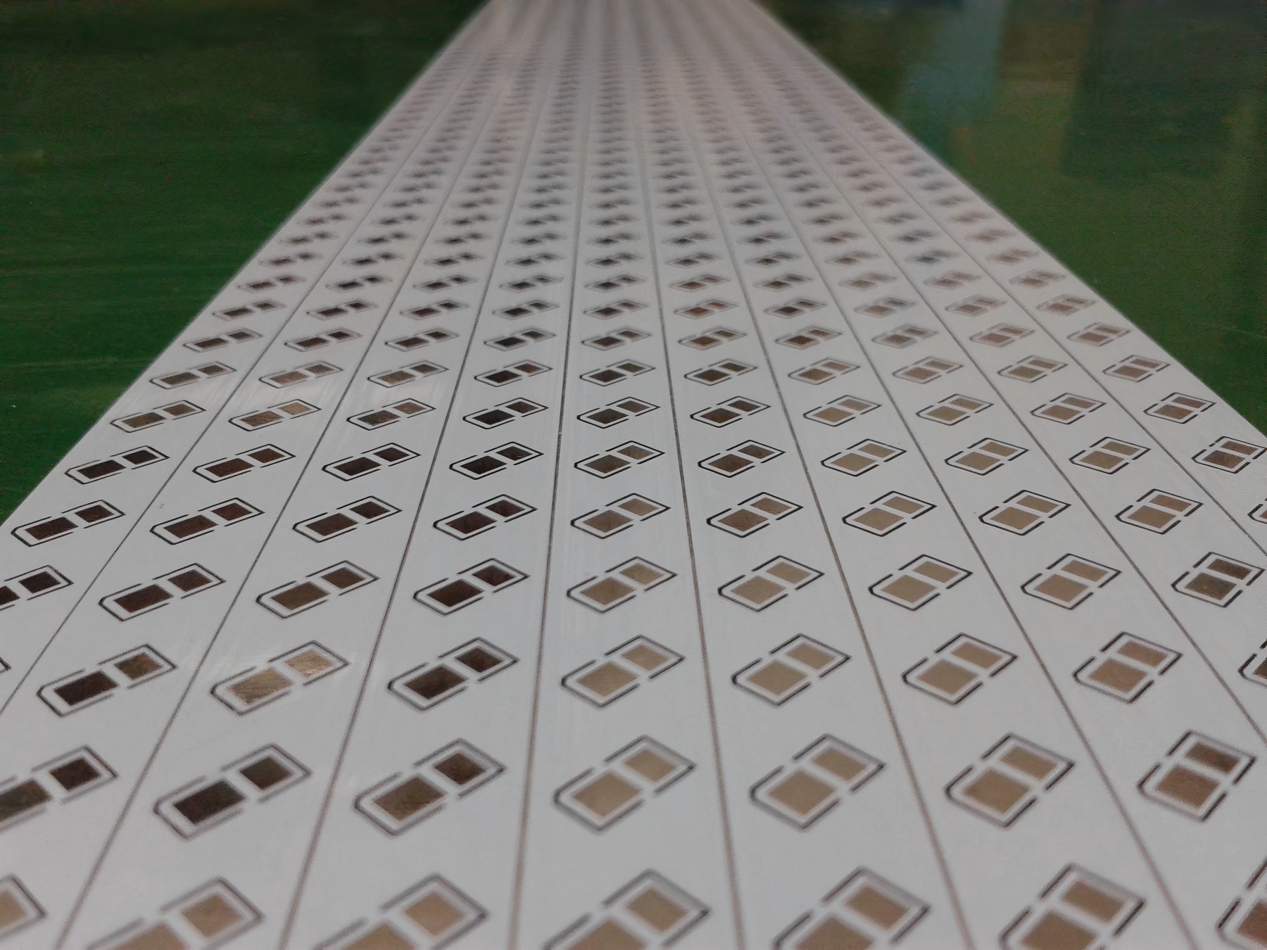
Pain Point 3: Delays in Production and DeliverySolution: With a monthly production capacity of 260,000 square feet, we handle both small prototypes and large-volume orders. Urgent LED Street Light Aluminum PCB orders can be shipped within 24 hours, meeting tight project deadlines.
Pain Point 4: Difficulty Customizing for Specific Street Light DesignsSolution: We offer fully customizable LED Street Light Aluminum PCB, including aluminum base thickness, copper weight, dielectric material, and surface finish. Our engineering team works with you to optimize designs for your specific street light requirements.
Pain Point 5: Unreliable Supply Chain for ComponentsSolution: EBest has a stable, global supply chain for all components needed for LED Street Light Aluminum PCB, ensuring we never face shortages. This stability means consistent production and on-time delivery for your orders.
Don’t let these pain points derail your LED street light projects. Choose EBest for LED Street Light Aluminum PCB solutions that solve your biggest challenges—contact us today to get started.
What Are the Key Design Tips for LED Street Light Aluminum PCB?
Designing an effective LED Street Light Aluminum PCB requires attention to thermal management, layout, and material selection. Follow these tips to ensure optimal performance and durability.
- Prioritize thermal path design: Place LED chips directly above the aluminum base to minimize thermal resistance. Use thermal vias to connect the circuit layer to the aluminum base for faster heat transfer.
- Choose the right aluminum alloy: For most street lights, 1060 or 6061 aluminum is ideal—1060 for high thermal conductivity, 6061 for better mechanical strength.
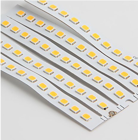
- Optimize copper weight: Use 2–3oz copper for high-power street lights (50W+); 1oz copper works for low-power applications. Thicker copper improves heat dissipation and current carrying capacity.
- Select a durable dielectric layer: Use ceramic-filled epoxy dielectric (1.0–3.0 W/m·K) for outdoor use, as it resists moisture, corrosion, and temperature fluctuations.
- Leave adequate spacing: Ensure 0.5mm+ spacing between LED chips and traces to prevent overheating and signal interference.
How to Test the Quality of LED Street Light Aluminum PCB Before Use?
Testing LED Street Light Aluminum PCB before integration is critical to avoid costly failures. Follow these simple, effective tests to verify quality and performance.
Test 1: Thermal Resistance TestUse a thermal imaging camera to measure the board’s surface temperature under load. A quality LED Street Light Aluminum PCB should have a surface temperature below 65℃ when powering a 50W LED.
Test 2: Insulation Resistance TestUse a megohmmeter to test insulation between the circuit layer and aluminum base. The resistance should be ≥10¹²Ω to ensure no electrical leakage, critical for outdoor safety.
Test 3: Mechanical Strength TestCheck the board’s bending strength—1.6mm thick LED Street Light Aluminum PCB should withstand 150MPa of force without bending or cracking, ensuring durability in outdoor installations.
Test 4: Corrosion Resistance TestExpose the board to salt spray for 24 hours. A quality board will show no signs of corrosion on the aluminum base or circuit layer, ensuring longevity in coastal or humid areas.
What Are the Latest Innovations in LED Street Light Aluminum PCB Technology?
The LED Street Light Aluminum PCB industry is constantly evolving, with new innovations focused on better thermal performance, durability, and sustainability. Here are the latest advancements to watch in 2026.
Innovations 1: High-Thermal Dielectric MaterialsNew ceramic-filled dielectric materials (up to 8 W/m·K) improve heat transfer by 200% compared to traditional dielectric layers, reducing junction temperatures by 15–20℃ for even longer LED lifespan.
Innovations 2: Multilayer Aluminum PCBsMultilayer LED Street Light Aluminum PCB allows for more complex circuit designs, integrating power management and control circuits on a single board, reducing size and improving efficiency.
Innovations 3: Sustainable Aluminum AlloysRecycled aluminum alloys with the same thermal conductivity as virgin aluminum are now used in LED Street Light Aluminum PCB, reducing environmental impact without compromising performance.
Innovations 4: Smart Thermal MonitoringSome advanced LED Street Light Aluminum PCB include built-in thermal sensors, allowing real-time monitoring of board temperature and proactive maintenance alerts, reducing downtime.
What Services and Certifications Does EBest Offer for LED Street Light Aluminum PCB?
EBest provides comprehensive services and holds industry-leading certifications to ensure our LED Street Light Aluminum PCB meets the highest standards of quality and reliability.
Our Core Services for LED Street Light Aluminum PCB
- Custom Design & Prototyping: Tailor-made LED Street Light Aluminum PCB designs based on your specific requirements, with fast prototype turnaround.
- Full Turnkey Production: End-to-end production from component sourcing to final assembly, saving you time and effort.
- Quick Turn Service: Urgent LED Street Light Aluminum PCB orders shipped within 24 hours, ideal for tight project deadlines.
- Component Supply: Stable supply chain for all electronic components needed for your LED Street Light Aluminum PCB.
- Post-Sale Support: Technical assistance and troubleshooting to ensure your LED Street Light Aluminum PCB performs optimally.
EBest Quality Certifications
| Certification | Relevance to LED Street Light Aluminum PCB |
|---|---|
| IATF 16949 | Ensures compliance with automotive and industrial lighting quality standards, critical for durable street lights. |
| ISO 9001:2015 | Guarantees consistent production processes and quality control for every LED Street Light Aluminum PCB. |
| ISO 13485:2016 | Meets medical-grade quality standards, ensuring high reliability for critical outdoor lighting applications. |
| AS9100D | Complies with aerospace-grade quality requirements, reflecting our commitment to extreme reliability. |
| REACH | Ensures our LED Street Light Aluminum PCB is free from harmful substances, safe for the environment. |
| RoHS | Complies with global environmental standards, making our PCBs suitable for international markets. |
| UL | Guarantees electrical safety, critical for outdoor lighting systems exposed to weather and public use. |
Why Should You Choose EBest for LED Street Light Aluminum PCB? (Quality, Delivery, Service & More)
When it comes to LED Street Light Aluminum PCB, EBest stands out from competitors with our unwavering focus on quality, speed, and customer satisfaction. Here’s why we’re the top choice for businesses worldwide.
Uncompromising QualityOur LED Street Light Aluminum PCB uses A+ grade materials, strict quality control, and 100% full inspection before delivery. We invest heavily in R&D to stay ahead of industry trends, ensuring our boards meet the latest performance standards.
Fast, Reliable DeliveryWith a monthly production capacity of 260,000 square feet, we handle orders of all sizes. Urgent LED Street Light Aluminum PCB orders are shipped within 24 hours, and standard orders are delivered on time, every time.
Stable Supply ChainOur dedicated purchasing team maintains a stable, global supply chain for all components needed for LED Street Light Aluminum PCB, eliminating shortages and delays.
Customized ServiceWe offer fully customizable LED Street Light Aluminum PCB designs, tailored to your specific street light requirements. Our engineering team provides personalized support to optimize your design for performance and durability.
19+ Years of ExpertiseFounded in 2006, EBest has over 19 years of experience in PCB manufacturing, making us a trusted partner for clients worldwide. We understand the unique challenges of LED Street Light Aluminum PCB and deliver solutions that work.
FAQ: Common Questions About LED Street Light Aluminum PCB
Below are the most frequently asked questions about LED Street Light Aluminum PCB, with clear, concise answers to help you make informed decisions.
Q1: What is the typical lifespan of LED Street Light Aluminum PCB?A1: The typical lifespan of LED Street Light Aluminum PCB is 50,000+ hours when used in standard outdoor conditions. This translates to 5–7 years of continuous operation, depending on the LED power and environmental factors. Our boards are designed to match the lifespan of high-quality LED chips, reducing maintenance costs.
Q2: Can LED Street Light Aluminum PCB be used in cold or hot climates?A2: Yes, LED Street Light Aluminum PCB is designed for extreme temperatures, with an operating range of -40℃ to 85℃. The aluminum base and durable dielectric layer resist thermal expansion and contraction, ensuring stable performance in both cold and hot climates—from snowy winters to scorching summers.
Q3: Is LED Street Light Aluminum PCB compatible with smart lighting systems?A3: Yes, our LED Street Light Aluminum PCB is fully compatible with smart lighting systems. We can customize the board to integrate sensors, dimming controls, and wireless communication modules, allowing for remote monitoring and control of street lights.
Q4: How long does it take to produce LED Street Light Aluminum PCB at EBest?A4: Production time for LED Street Light Aluminum PCB depends on order size. Prototypes are ready in 1–3 days, standard orders (100–1000 units) take 5–7 days, and large-volume orders take 10–14 days. Urgent orders can be shipped within 24 hours for time-sensitive projects.
Q5: Can I get a custom size for LED Street Light Aluminum PCB?A5: Yes, EBest offers fully customizable sizes for LED Street Light Aluminum PCB. We can produce boards in any size, from small prototypes to large panels, to match your street light design. Our engineering team will work with you to optimize the size for thermal performance and installation.
Q6: Does LED Street Light Aluminum PCB require special installation?A6: No, LED Street Light Aluminum PCB uses standard installation methods, compatible with most street light fixtures. The aluminum base is lightweight and easy to mount, and the board’s design ensures compatibility with standard LED chips and power supplies. We provide installation guidelines to ensure a smooth process.
Q7: How does LED Street Light Aluminum PCB reduce maintenance costs?A7: LED Street Light Aluminum PCB reduces maintenance costs by improving LED lifespan and stability. Its superior heat dissipation prevents premature LED failure, reducing the need for frequent replacements. Additionally, our strict quality control ensures minimal defects, further lowering maintenance efforts and costs.
How to Select the Right Thickness for LED Street Light Aluminum PCB?
Choosing the right thickness for LED Street Light Aluminum PCB is critical for performance and durability. The thickness depends on LED power, installation method, and environmental conditions.
Guidelines for Thickness Selection
- Low-power street lights (10–30W): 1.0–1.2mm aluminum base—lightweight and cost-effective for small fixtures.
- Medium-power street lights (30–50W): 1.6mm aluminum base—balances thermal performance and mechanical strength.
- High-power street lights (50–100W): 2.0–3.0mm aluminum base—provides superior heat dissipation and durability for heavy-duty use.
EBest can help you select the ideal thickness for your LED Street Light Aluminum PCB based on your specific project requirements.
Get Your High-Quality LED Street Light Aluminum PCB from EBest Today
If you’re looking for reliable, high-performance LED Street Light Aluminum PCB that meets your design, quality, and delivery needs, EBest is your trusted partner. With 19+ years of expertise, industry-leading certifications, and customized solutions, we deliver PCBs that enhance your street light’s performance and durability.
We provide top-tier LED Street Light Aluminum PCB for all outdoor lighting applications. Whether you need prototypes, small batches, or large-volume orders, we have the capacity and expertise to deliver on time and to your exact specifications.
Place your order today by emailing us at sales@bestpcbs.com. Let EBest be your go-to source for LED Street Light Aluminum PCB—we’re here to help you succeed.