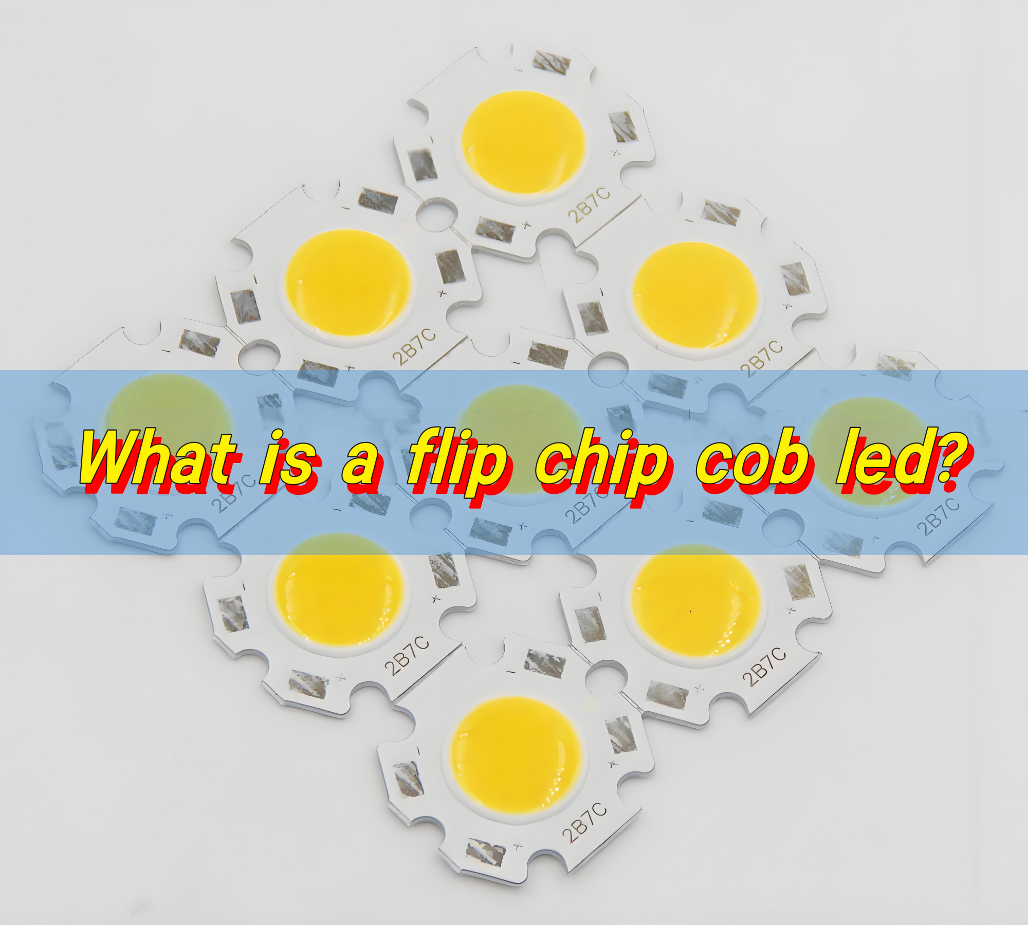
What is a full flip chip cob led? COB (Chip On Board), or chip on board packaging technology, is a technology that directly packages multiple LED chips on a circuit board. Unlike traditional LED packaging methods, COB LEDs do not need to package each chip separately, but instead arrange them closely and integrate them on a common substrate to form a light-emitting module.
What is a COB flip chip?
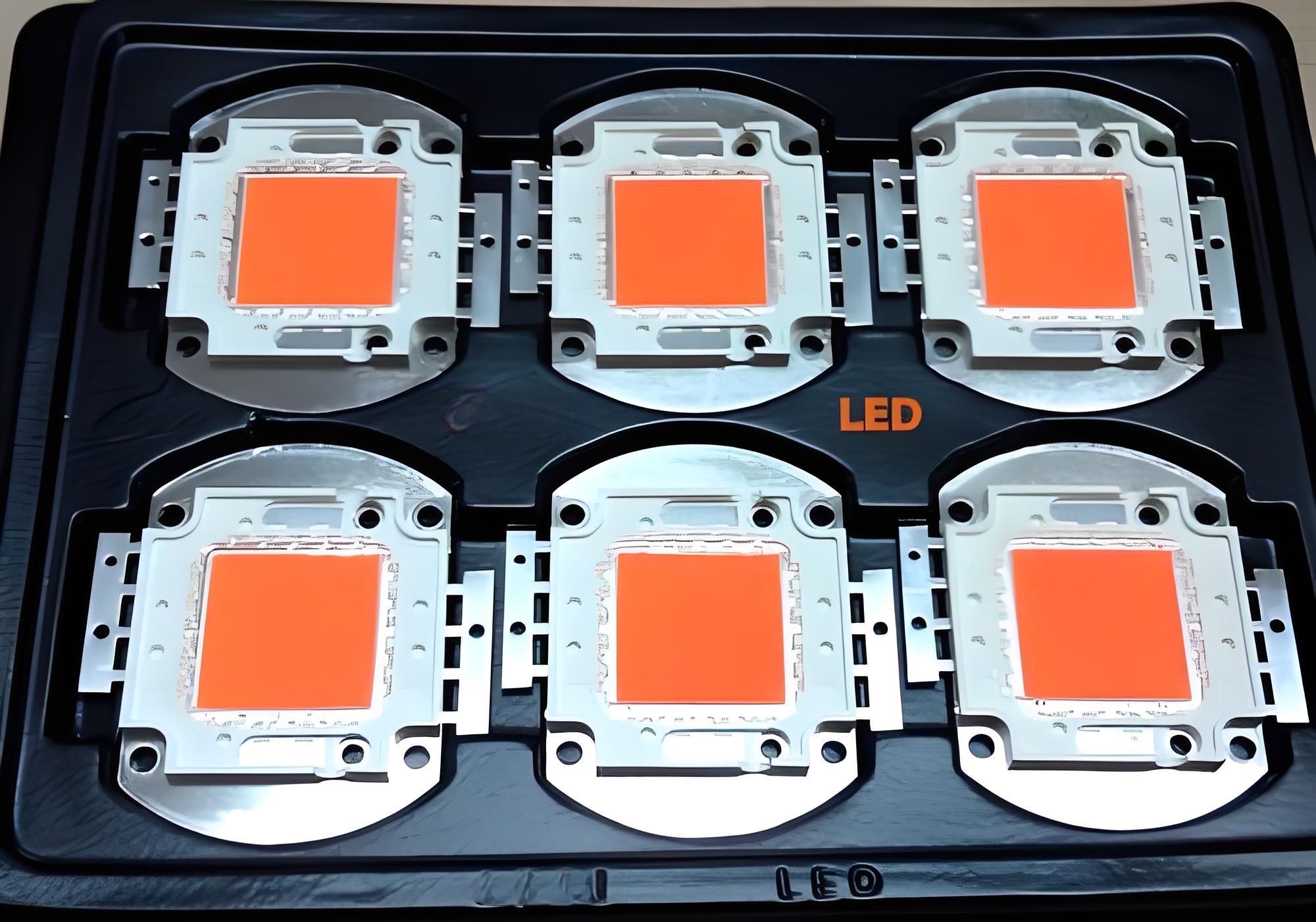
COB flip chip refers to a packaging technology, the full name of which is Chip on Board (chip directly on the board), where “flip” refers to the packaging method of the chip. Flip chip COB technology packages LED chips directly on the PCB substrate, covers the silicon wafer with thermally conductive epoxy resin, and performs heat treatment, and finally establishes an electrical connection between the chip and the substrate through wire bonding.
Its characteristics and applications:
- Simple structure: Full Flipped chip COB technology has a simpler structure, reduces gold or copper wire connections, and simplifies the manufacturing process.
- High temperature resistance: This packaging method has better high temperature resistance and improves the stability and reliability of the product.
- Good heat dissipation performance: Due to the reduction of connecting parts, the heat dissipation performance is improved, reducing the risk of dead lights and falling lights.
- Widely used: Flip-chip COB technology is widely used in indoor small-pitch LED displays.
Comparison with other packaging technologies
- Formal COB: The formal chip packaging method is earlier, the process is mature but the stability is poor, it is easily affected by moisture, and it affects the light output efficiency and heat dissipation efficiency.
- Mixed COB: Mixing formal and flip chips, taking into account cost and performance, is suitable for the transition stage.
What is a flip chip used for?
The main functions of flip chips include:
- Reduce signal delay and parasitic inductance: Flip chips are directly electrically connected to the pads of the package substrate through bumps, without the need for long bonding wires, so the signal path is shorter, which can effectively reduce signal delay and parasitic inductance.
- Improve heat dissipation performance: Since the chip is directly connected to the substrate through bumps, heat is more easily transferred to the substrate, thereby improving heat dissipation performance.
- High I/O pin density: Flip chips have higher I/O pin density, save area, and are suitable for high-performance and high-integration applications.
- Improve package reliability: Flip chips use metal ball connections, which are compact and reliable, so they are increasingly used in the packaging industry.
- Reduce package size: Using metal ball connections can reduce package size, improve electrical performance, and solve the problem that traditional packaging methods need to expand volume due to increased pin counts.
How does a flip-chip work?
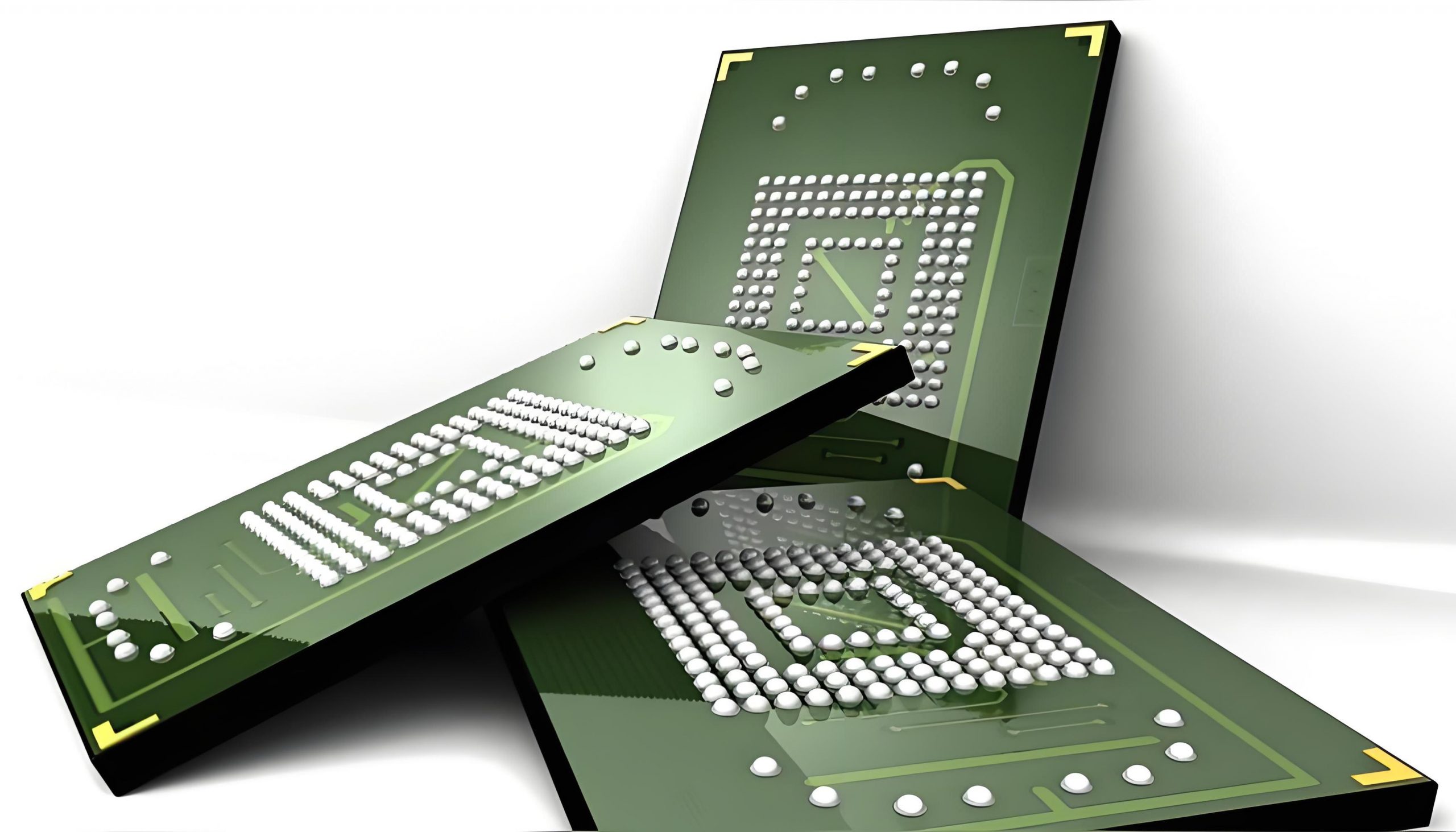
The working principle of flip chip technology is to form bumps on the active side of the chip, and then align and weld the active side of the chip with the pads on the substrate facing down, thereby achieving direct electrical connection between the chip and the substrate.
This connection method not only reduces the package volume, but also improves signal transmission speed and reliability because the signal path is shorter and the parasitic inductance and capacitance effects caused by wire bonding are avoided.
What are the disadvantages of flip chip?
The main disadvantages of flip chips include thermal stress problems and reliability problems. Due to the mismatch in the coefficient of thermal expansion (CTE) between the chip and the substrate, when the temperature changes, the solder joints will be subjected to large thermal stress, resulting in fatigue damage and failure. In order to solve these problems, the bottom filling process is usually adopted, that is, polymer materials are injected into the gap between the chip and the substrate to improve the stress distribution of the solder joint, reduce the strain amplitude, and extend the thermal fatigue life of the solder joint.
In addition, flip chip technology faces some challenges in practical applications, including:
- Material selection and process optimization: As chips become increasingly miniaturized and thinner, the requirements for the performance of filling materials and packaging reliability continue to increase. Material design, process optimization and other measures are effective ways to deal with potential challenges.
- Wide-scale use of lead-free solder: The use of lead-free solder has put forward new requirements for the bottom filling process, which requires further research and improvement.
What are the different types of flip chips?
There are mainly the following types of flip chips:
FCBGA (flip chip ball grid array package):
- Process characteristics: FCBGA uses small balls instead of pins for welding, has high I/O density, can effectively solve electromagnetic compatibility and electromagnetic interference problems, and reduce the packaging area. In addition, its good heat dissipation performance enables the chip to work stably at higher power.
- Application areas: Widely used in high-end microprocessor and graphics processing chip packaging, such as high-end CPU and GPU, to ensure the stability and performance of the chip when running at high frequency.
FCCSP (Flip Chip Size Package):
- Process characteristics: FCCSP can achieve chip size and package size close to each other, suitable for portable electronic devices with strict space requirements. Its compact packaging form minimizes the space occupied by the package while ensuring chip performance.
- Application areas: Suitable for devices with limited internal space such as smartphones and tablets, which can reduce the package space while ensuring performance, leaving more space for other components.
Cob flip chip vs smd
SMD and COB each have their own advantages and disadvantages. Which technology to choose depends on the specific application scenario and requirements.
Application scenarios and comparison of advantages and disadvantages
1. Packaging method:
- SMD: SMD (Surface Mount Device) technology is to package LED chips into lamp beads and then solder them on the PCB board. This technology is mature and low-cost, and is suitable for LED displays with regular spacing.
- COB: COB (Chip-on-Board) technology is to directly package the LED chip on the PCB board, with a smaller dot pitch, which is suitable for micro-pitch LED display screens. Although the cost is higher, the process is simpler and the dot pitch can be smaller.
2. Dot pitch:
- SMD: The dot pitch is larger, usually reaching P20 to P1.25, but it is difficult to reduce further.
- COB: The dot pitch is smaller, suitable for products of P1.25 and below, such as P0.93, P0.78, etc.
3. Cost:
- SMD: Due to mature technology and low cost, it is suitable for large-scale production and conventional applications.
- COB: Due to the high cost of technology and materials, it is suitable for the high-end, high-demand micro-pitch LED display market.
4. Stability and life:
- SMD: Due to the protrusion of the lamp beads, it is easy to cause the problem of falling or dead lights during installation and removal.
- COB: Directly encapsulated on the PCB board, the probability of falling and dead lights is reduced, and the stability is better.
5. Optical performance and heat dissipation performance:
- SMD: The light spot may be uneven due to the independent light emission of multiple LED chips, and the color rendering performance is affected by the design and materials. Heat dissipation performance is affected by the packaging design of a single LED chip.
- COB: Multiple LED chips are closely arranged, the light spot is uniform, the color rendering performance is good, and the heat dissipation area is large and uniform.
What is the difference between flip chip and BGA?
The main difference between flip chip (Flip Chip) and BGA (Ball Grid Array) lies in the packaging method and application scenario.
1. Packaging method
- Flip chip (Flip Chip): Flip chip is a packaging technology that directly solders the contact points of the chip to the substrate. The contact points of the chip (usually metal balls) are directly connected to the contacts on the substrate to form an electrical connection.
- BGA (Ball Grid Array): BGA is a surface mounting technology in which the chip is connected to the pads on the substrate through its contact points (usually ball pins). BGA packaging usually uses a solder ball array, and the solder balls are fixed to the substrate by reflow soldering.
2. Application scenarios and advantages and disadvantages
Flip chip:
- Advantages: Reduced resistance and parasitic capacitance, increased signal transmission speed; small package size, suitable for high-density integration; high reliability because of reduced connection points.
- Disadvantages: Complex manufacturing process and high cost; requires precise alignment and welding technology.
- Application scenarios: Suitable for high-performance computing and high-speed signal transmission occasions, such as CPU, GPU, etc.
BGA:
- Advantages: Increased I/O pin count and increased packaging density; increased assembly yield; improved electrothermal performance.
- Disadvantages: Occupies a large substrate area; relatively complex manufacturing process and high cost.
- Application scenarios: Suitable for high pin count and high performance requirements, such as high-end processors, graphics processing units, etc.
What is the difference between flip chip and COB?
Flip chip and COB (Chip on Board) have significant differences in definition and application.
1. Definition and basic concepts
- Flip chip is a chip packaging technology in which the I/O end (pin) of the chip faces downward and is connected to the substrate through solder bumps. This technology can improve packaging density and electrical performance, and is often used in high-performance computing and communication equipment.
- COB (Chip on Board) is a technology that directly packages chips on circuit boards, aiming to solve the shortcomings of traditional LED displays, such as dead lights and falling lights, and improve stability and resolution. COB technology is divided into two types: positive and flip.
2. Packaging method:
- Flip chip: The I/O end of the chip faces down and is connected to the substrate through solder bumps.
- COB: The chip is directly packaged on the PCB board, which is divided into positive and flip. The positive chip faces up and is connected through welding wires; the flip chip faces down and is directly connected to the PCB without welding wires.
3. Application field:
- Flip chip: Widely used in high-performance computing, communication equipment and other fields, it is favored for its high-density installation and good electrical performance.
- COB: Mainly used in LED displays, especially in the field of high-end displays. COB technology can solve the problems of high thermal resistance, high cost and smaller spacing in traditional SMD packaging.
4. Advantages and Disadvantages:
- Flip chip: Advantages include high packaging density and good electrical performance; Disadvantages are complex production process and high cost.
- COB: Formal COB has lower cost, but there are wire bonding problems that affect stability and heat dissipation efficiency; Flip chip COB has high process requirements, better stability, strong thermal conductivity, but higher cost.
Flip chip COB LED integrates the advantages of COB packaging and flip chip technology, achieving precise light color control and uniform light distribution in optical performance, excellent electrical performance, efficient heat dissipation, and strong stability. As a professional PCB manufacturer, BEST Technology is committed to creating high-quality PCBs for flip chip COB LEDs and providing stable and reliable solutions.