What Is Solder Mask?
A solder mask also called solder resist, it is a protective layer applied to a printed circuit board (PCB) to shield copper traces from oxidation, contamination, and unintended solder bridges. Without this layer, exposed copper can easily corrode or cause short circuits due to accidental solder connections.
Most solder masks are made from epoxy resins, liquid photo imageable (LPI) materials, or dry films. These materials create an insulating layer that only exposes the necessary contact points for soldering, such as component pads. In modern PCB manufacturing, solder masks are essential for ensuring proper functionality, ease of assembly, and long-term reliability. Whether for simple or advanced circuits, a high-quality solder mask is critical for maintaining the integrity of a PCB.
How Is Solder Mask Applied to Your PCB?
How is solder mask applied to your PCB? Applying a solder mask is a multi-step process that requires precision to ensure even coverage and proper functionality. The process varies depending on the type of solder mask used, but the general steps include:
1. Surface Preparation
Before applying a solder mask, the PCB surface must be thoroughly cleaned. Any dust, grease, or oxidation can affect adhesion. Manufacturers use chemical cleaning or mechanical scrubbing to remove contaminants and prepare the board for coating.
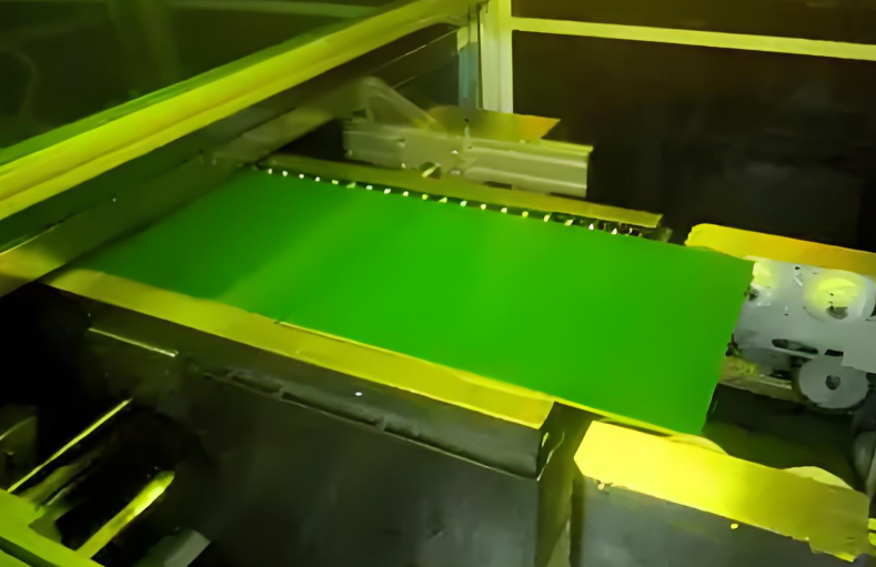
2. Solder Mask Application
The solder mask is applied using one of the following methods:
- LPI Solder Mask: A liquid mask is sprayed or screen-printed onto the PCB surface. This method provides excellent precision and is widely used in high-density PCB designs.
- Dry Film Solder Mask: A pre-cured solder mask film is laminated onto the board and then exposed to UV light for patterning. It is a common method in high-volume manufacturing.
- Epoxy-Based Solder Mask: A thermosetting polymer is screen-printed onto the board and then cured. This is one of the oldest methods but is less precise than LPI.
3. UV Exposure and Developing
After application, the board is exposed to ultraviolet (UV) light through a photomask that defines the solder mask openings. The exposed areas harden, while the unexposed parts remain soft and can be removed using a developer solution.
4. Curing and Final Inspection
Once the mask is developed, the PCB undergoes a curing process, usually in an oven, to fully harden the solder mask. Afterward, the board is inspected to ensure the mask is properly applied without defects. Evenly application of the solder mask is essential for preventing soldering issues and ensuring the long-term reliability of the PCB.
Why Is the Solder Mask Green?
The green color of solder masks became the industry standard due to a combination of historical, practical, and technical factors. Early PCB manufacturing processes used epoxy-based resins, which naturally had a green tint. Over time, manufacturers standardized this color because it offered excellent contrast for visual inspection. Engineers and technicians rely on automated optical inspection (AOI) systems to detect defects, and the green color provides the best balance between visibility and eye strain. Other colors like red, blue, and black exist, but green remains the most widely used due to its well-established reliability and cost-effectiveness.
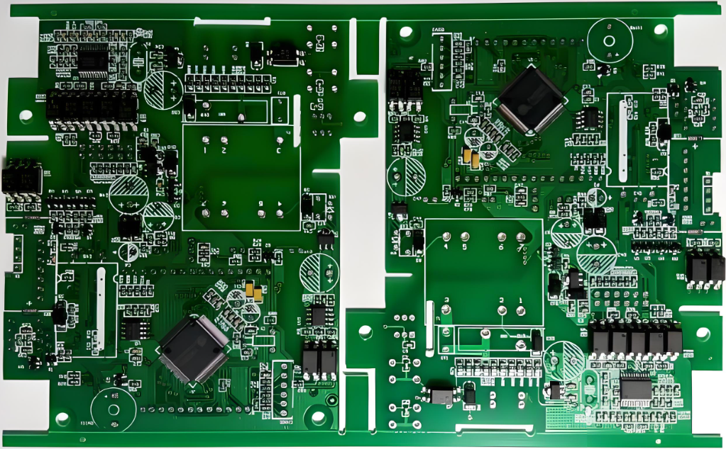
Beyond visibility, green solder masks also offer superior thermal and chemical stability compared to some other colors. PCBs endure high temperatures during soldering, and green formulations have been extensively tested to withstand heat without degrading.
What Can I Use Instead of a Solder Mask Material?
If a solder mask isn’t available, there are alternative methods to protect PCB copper traces. However, they may not provide the same level of durability and precision.
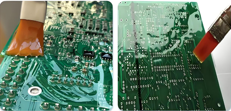
1. Conformal Coatings
Conformal coatings are thin protective layers applied to PCBs to protect against moisture, dust, and corrosion. While they don’t replace solder masks, they can provide an extra layer of protection. Some PCBAs may required to coating a layer of conformal as an extra protect layer.
2. Kapton Tape
Kapton tape is a heat-resistant, electrically insulating material that can be used to protect specific areas of a PCB. However, it doesn’t offer the same level of coverage or durability as a solder mask.
3. PCB Lacquers
Some manufacturers use specialized PCB lacquers to coat copper traces and prevent oxidation. These coatings are easy to apply but may wear off over time.
4. DIY Solutions
Some electronics hobbyists use clear nail polish as a temporary solder mask substitute. While it can offer short-term protection, it is not a recommended solution for professional PCBs.
A proper solder mask is always the best choice for ensuring the longevity and reliability of a PCB.
How Do You Apply Solder Mask Evenly?
A smooth and uniform solder mask application is crucial for avoiding defects. Here are some key factors to consider:
1. Clean the PCB Surface: Any dust or grease can cause uneven adhesion. Proper cleaning ensures the mask spreads evenly.
2. Use Controlled Application Methods: Automated spraying, screen printing, or laminating techniques help distribute the solder mask uniformly.
3. Maintain Proper Viscosity: If the solder mask is too thick or too thin, it may not spread evenly. Maintaining the right consistency ensures better coverage.
4. Ensure Proper Curing: Over-curing or under-curing can create issues with adhesion and durability. Controlled UV exposure and thermal curing help achieve the best results.
What Is the Solder Mask Requirement?
Solder mask requirements vary depending on PCB design, industry standards, and application needs. The mask must very good to protect the board from oxidation, solder bridges, and contaminants. Manufacturers should follow strict guidelines to ensure the solder mask meets performance and quality expectations. And customers also can inspect these parameters to make sure solder mask is good.
1. Thickness Requirements
The solder mask must maintain a consistent thickness to prevent defects. Typical thickness values are:
- Over Copper Traces: 15–35 μm (micrometers)
- Over Substrate (Bare Board Areas): 5–15 μm
- Near SMD Pads and Through-Holes: Sufficient clearance to avoid interference with soldering.
An uneven or excessively thick mask can cause soldering issues, while a thin mask may not provide enough protection.
2. Registration Accuracy
The solder mask must align precisely with the PCB layout. Misalignment can lead to:
- Blocked SMD pads or vias, affecting solderability.
- Unprotected traces, increasing the risk of oxidation or short circuits.
Industry standards, such as IPC-6012, define the allowable misregistration, typically within ±3 mils (±0.075 mm) to ensure proper coverage.
3. Clearance and Openings
The solder mask must be designed with appropriate clearances around pads and vias to ensure smooth soldering. Key points include:
- Pad-to-solder mask clearance: Typically 3–5 mils (0.075–0.125 mm) to prevent solder mask from covering pad edges.
- Via coverage: Some designs require tenting (fully covering the via), while others leave vias exposed for better connectivity.
4. Electrical Insulation Properties
Solder masks act as an insulating layer to prevent short circuits between copper traces. The dielectric strength must be high enough to withstand PCB operating voltages. Common requirements include:
- Dielectric strength: Above 500V/mil for proper insulation.
- Surface resistivity: Greater than 10⁹ Ω/sq to prevent leakage currents.
5. Compliance with Industry Standards
Solder mask materials and application processes must comply with international standards, such as: IPC-SM-840, RoHS & REACH, UL 94V-0.
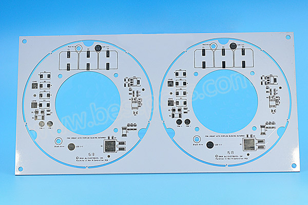
What Kinds of Solder Masks Do We Have in EBest Circuit (Best Technology)?
At EBest Circuit (Best Technology), we offer a range of solder masks to suit different PCB applications. Our selection includes:
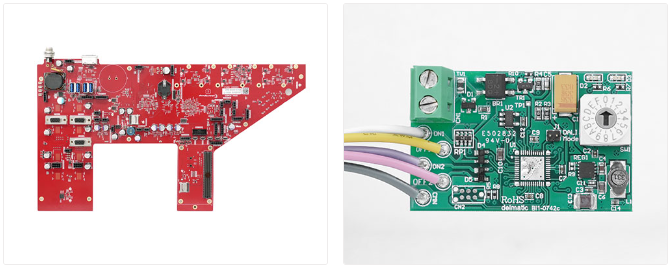
- Green (commonly select)
- Red (for prototype)
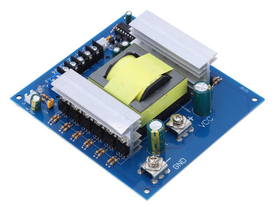
- Blue (for power supply board)
- Black (consumer electronics)
- Matte Black (high-end products or prototypes)
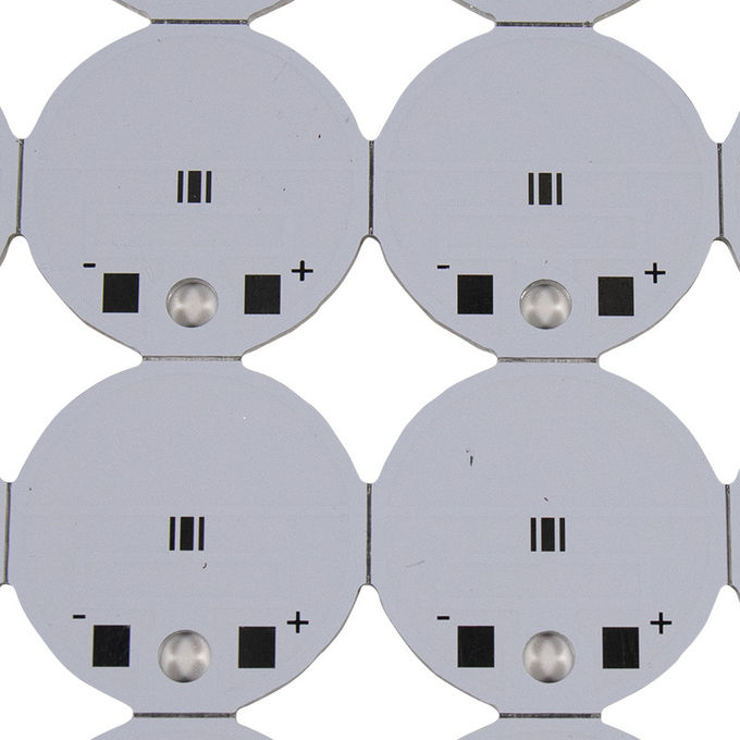
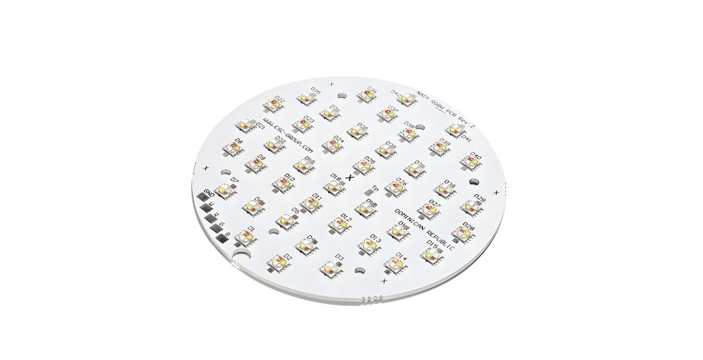
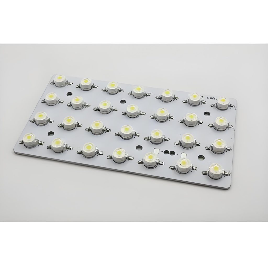
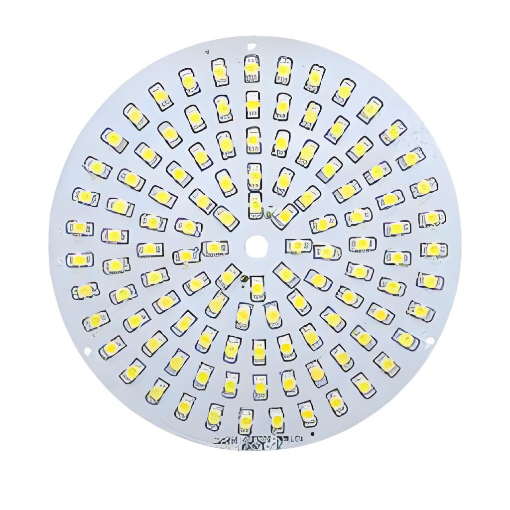
- White (lightings)
- Grey (prototypes)
- Matte Grey (prototypes)
- Yellow (rarely used)
- Purple (prototype or high-end product that need good appearance)
We ensure that our solder masks meet industry standards, providing excellent adhesion, thermal stability, and long-term reliability. Would you like to discuss a specific solder mask for your PCB project? Contact us today!