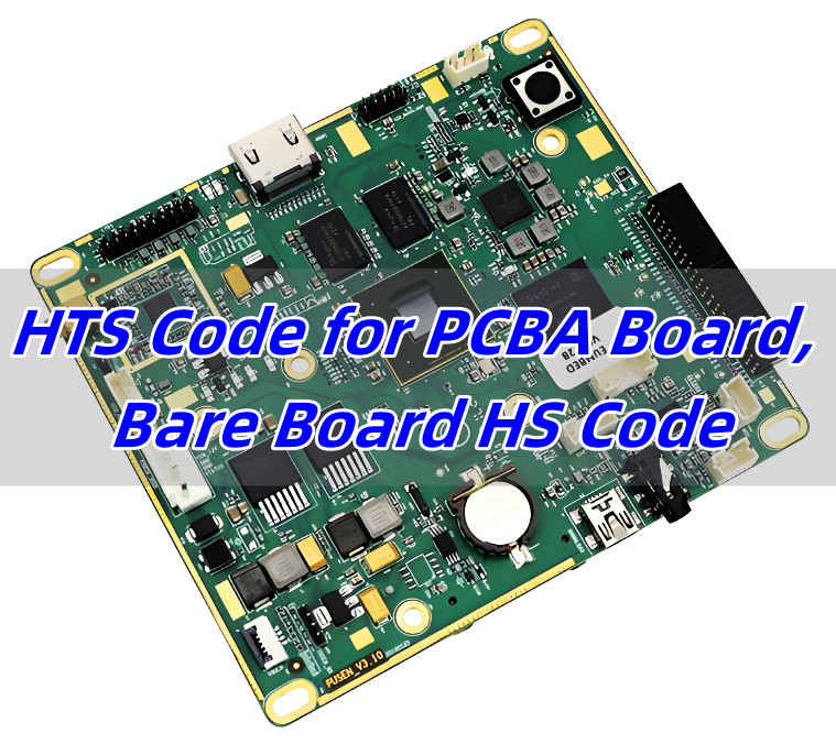
The HTS code for PCBA boards often fall under headings in Chapter 85, particularly sections dealing with electrical apparatus, but it doesn’t have a standard HS code cause it should depends on its function and purpose.
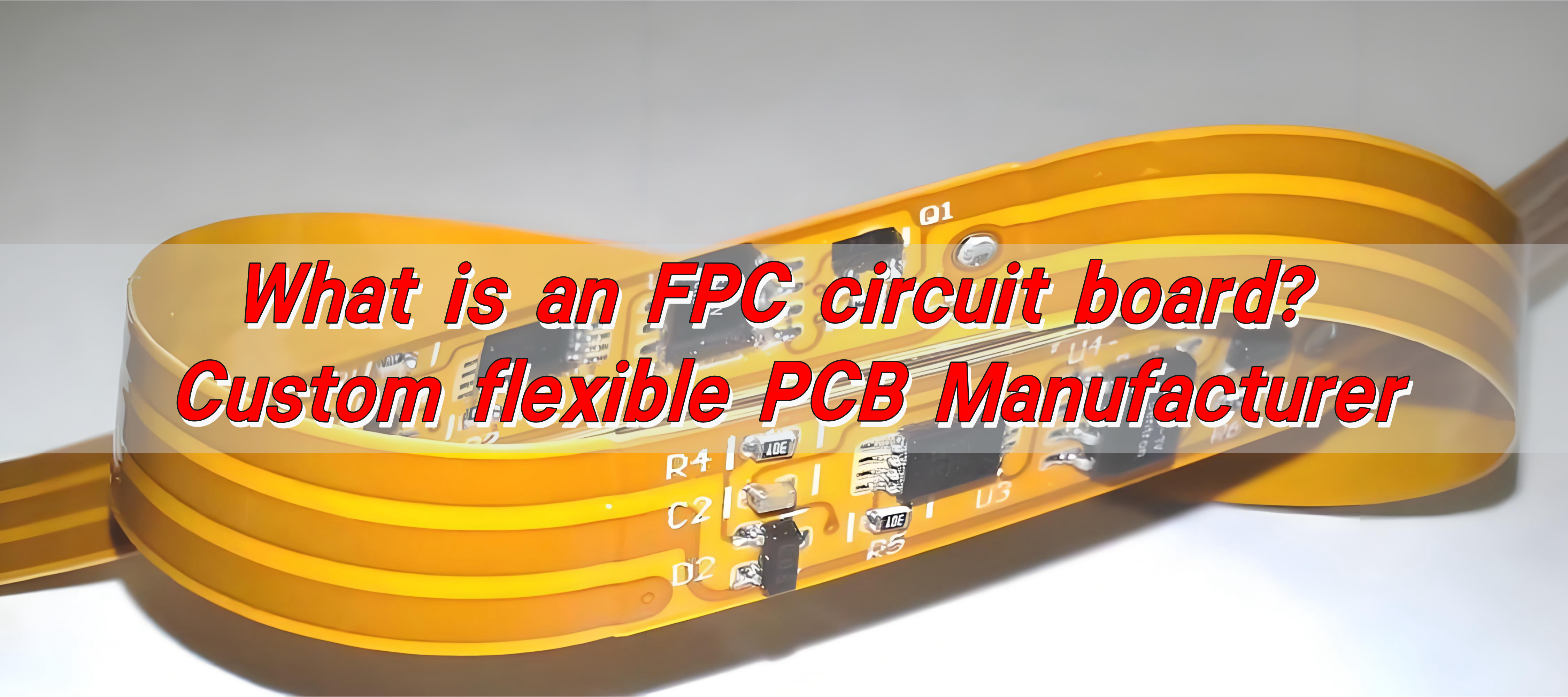
Understanding the HTS Code for PCBA Board is one of the most important steps in moving electronic assemblies across borders. This code tells customs how to classify a PCBA during import and export, and although the idea seems simple, the real process often causes uncertainty for buyers, logistics teams, and even engineers. The correct classification affects tariffs, clearance speed, and how your shipment is documented, so a solid grasp of HTS rules helps companies avoid delays and build a more predictable supply chain.
What Is HTS Code?
The HTS code, also called HS code or Harmonized Tariff Schedule code, is a numerical classification used by U.S. Customs for imports. It is based on the international Harmonized System (HS), which is managed by the World Customs Organization. These codes define how goods should be categorized during cross-border trade.
HTS is used in the United States, while many other countries use the six-digit HS format. The HTS expands those six digits into ten digits, offering more detailed classification for tariffs and trade control.
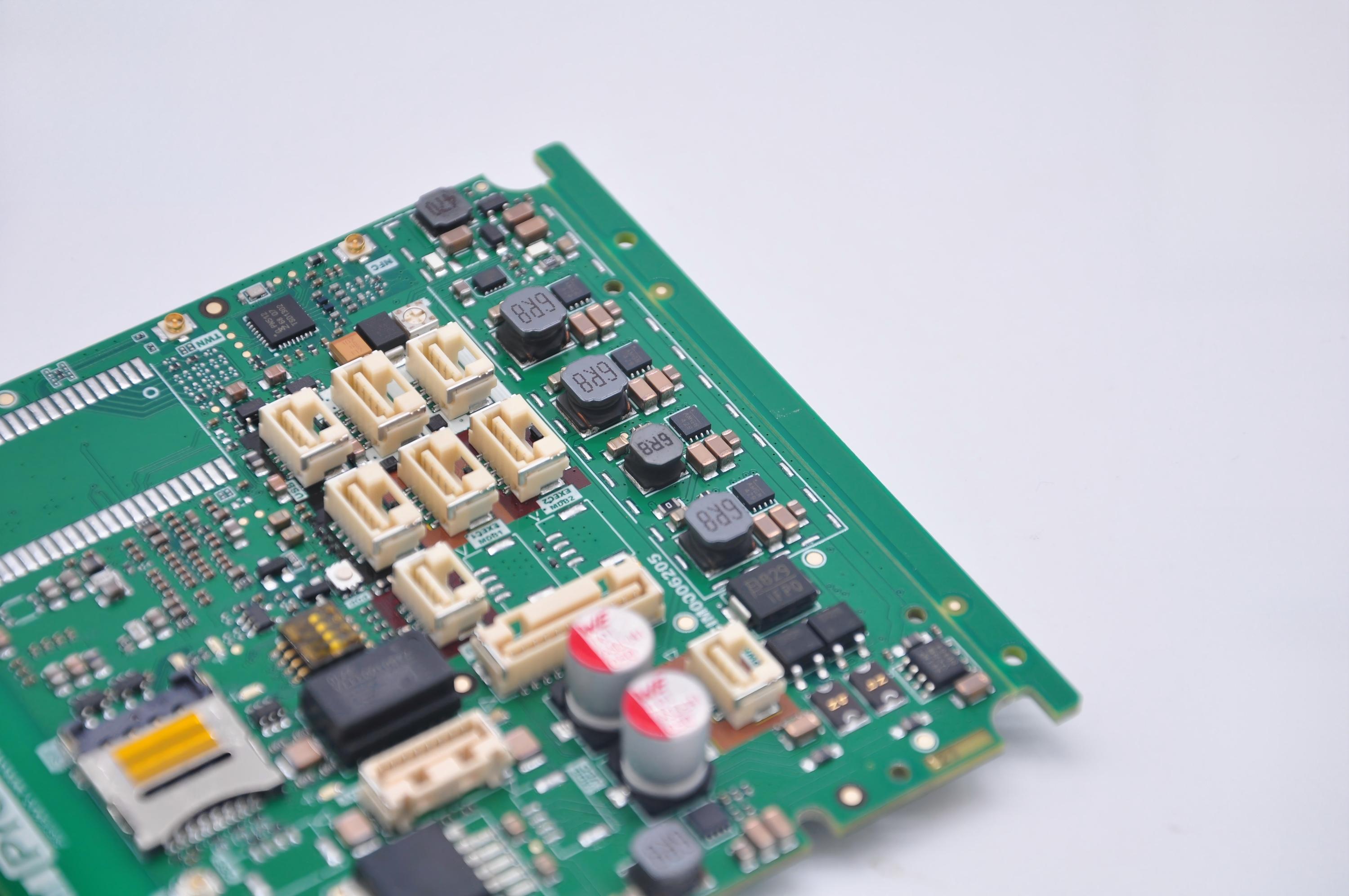
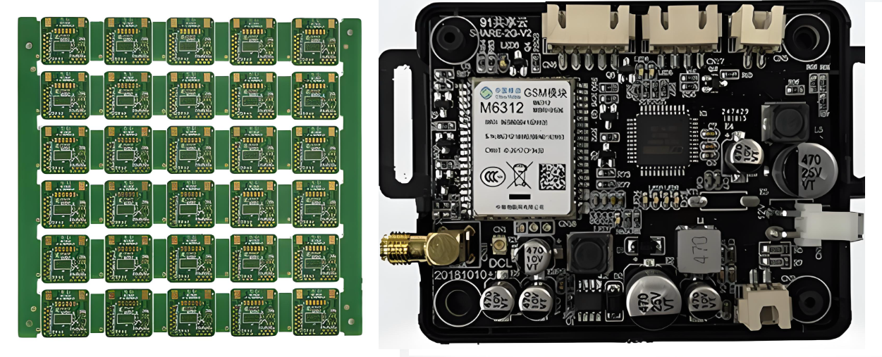
For electronic assemblies and PCBA shipments, an HTS code describes the board’s function, its degree of assembly, and how it will be used inside the final device. Although many companies assume there is only one standard code for PCBAs, classification actually depends on the product’s characteristics and end application.
In simple terms, HTS code = product identity in the customs system. It determines how the product is taxed, tracked, and cleared.
Why Correct HTS Code Is Important in International Trade?
Using the correct HTS code is a critical requirement for every international shipment. Customs authorities rely on the HS/HTS number to understand what the product is, how it should be taxed, and whether it has any special restrictions. When the code is accurate, shipments pass through customs faster and without extra checks.
The importance of accurate HTS classification lies in several areas:
- Accurate duty calculation
Tariffs depend entirely on the HTS code. Some codes have zero duty, while others carry higher rates. An incorrect code could lead to unexpected costs or disputes with customs authorities.
- Compliance and risk prevention
Incorrect classification may trigger delays, inspections, or even penalties. Customs departments may reclassify goods, creating extra paperwork and cost for importers.
- Proper trade documentation
Commercial invoices, packing lists, and declarations must use the right HTS code to match the product description. This consistency reduces the chance of errors during review.
- Avoiding future trade complications
Many companies are audited months or years after importing goods. A wrong HTS code can create issues long after the shipment has cleared.
For PCBA boards, correct classification also affects export compliance because some assemblies include RF modules, encryption components, or high-power devices. While the HTS code focuses on customs, an accurate description supports broader trade requirements.
How to Classify Electronic Board HS Code?
Classifying electronic boards requires a clear understanding of the product’s function. Customs classification is not based on the component list alone. Instead, the primary purpose of the board determines the HS code.
To classify any electronic board, the following factors are considered:
1. Is the board bare or assembled?
Bare PCBs and PCBAs fall under different HS categories. A bare copper-clad laminate with etched traces belongs to one code. Once components are mounted, the board is treated as an electronic module or a part of another machine.
2. What is the board used for?
Function is the central element in HS classification. Customs asks what device the PCBA belongs to:
- A control module
- A communication device
- A power supply
- A medical instrument
- An automotive controller
- A home appliance module
Each category may match a different HTS subheading.
3. Does the board perform a complete function or act as a part?
Some PCBAs operate as standalone electronic devices. Others are only subassemblies. Customs will place standalone units and internal modules in different HS categories.
For example:
- A PCBA that serves as a complete power supply may fall under power supply device codes.
- A PCBA used as a part inside a larger machine is classified as a “part of” that machine.
Common HS Codes for PCBA & PCB
When importing or exporting PCB and PCBA products, several HS codes are frequently used. While the final code always depends on product function, here are the most common categories buyers encounter.
Common HS Code for Bare PCB (Unassembled)
Bare printed circuit boards usually fall under:
- HS 8534.00 – Printed circuits
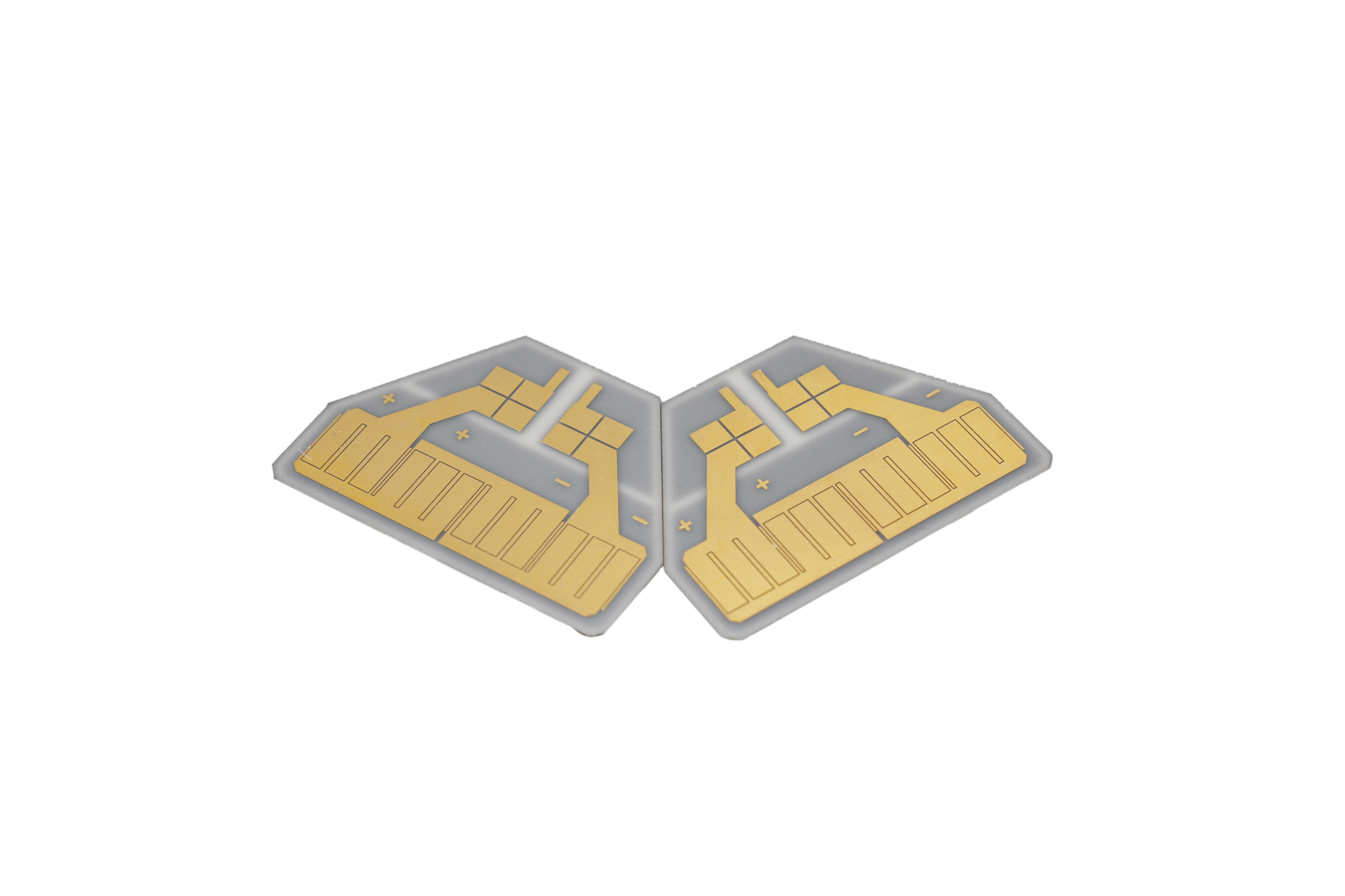
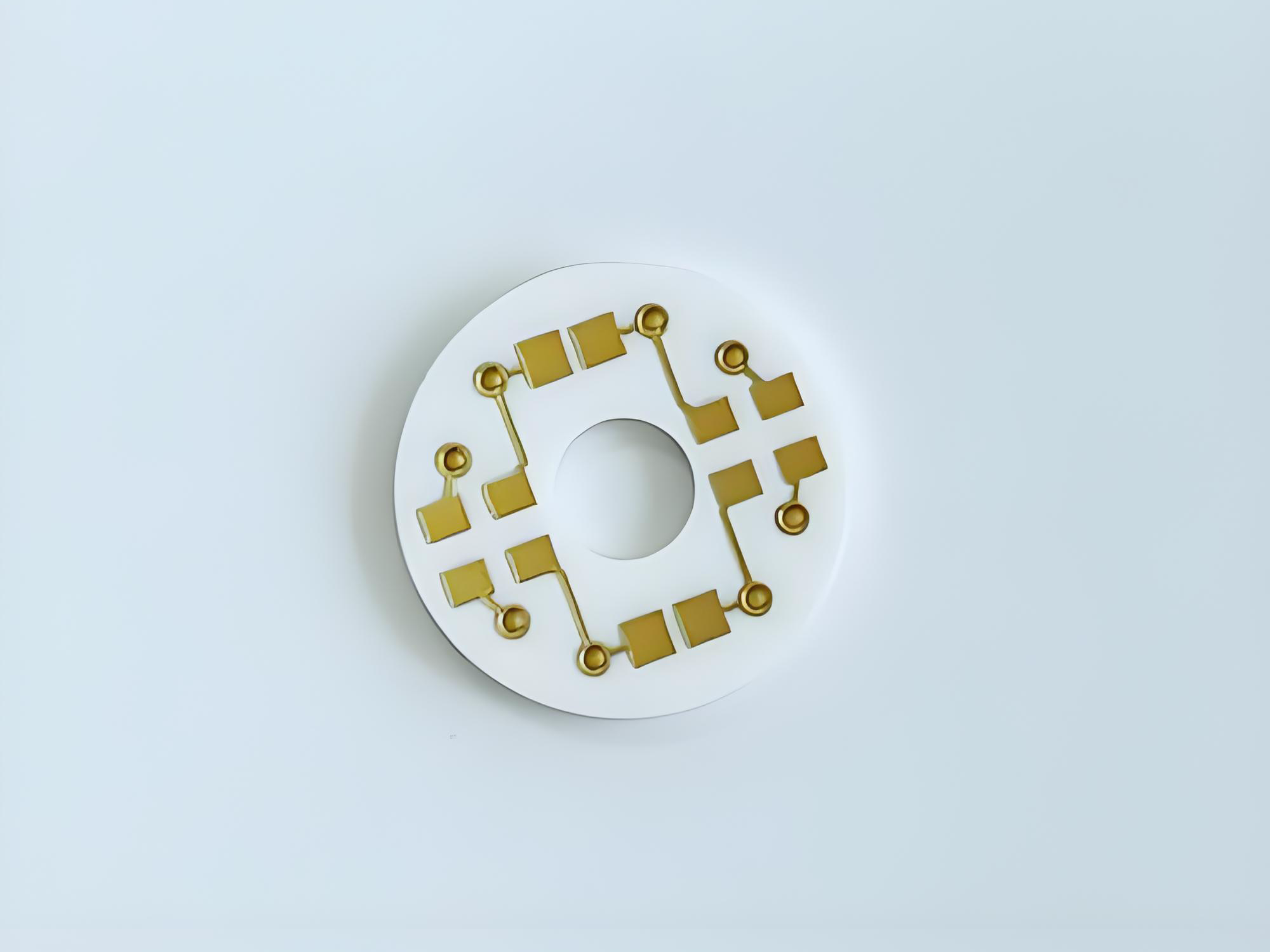
This covers rigid boards, flexible boards, metal-core PCBs, ceramic PCBs, and hybrid structures without mounted components.
Bare Board HS Code
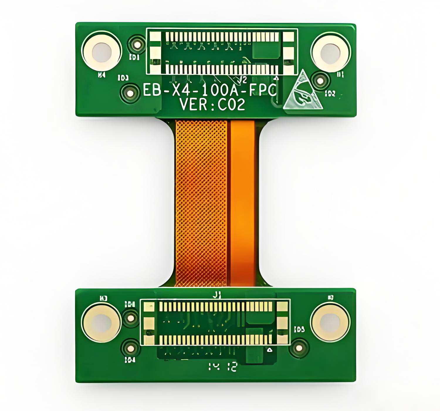
Common HS Codes for PCBA (Assembled Boards)
PCBAs often fall under headings in Chapter 85, particularly sections dealing with electrical apparatus.
Common examples include:
- HS 8538.90 – Parts suitable for use with equipment of 8535/8536
Often used for control boards, relay boards, switch assemblies, and modules used inside electrical equipment.
- HS 8504.90 – Parts of electrical transformers and power supply units
Used for PCBA boards functioning as power supply modules.
- HS 8543.90 – Parts of other electronic apparatus
Covers general-purpose electronic assemblies not specifically addressed in other HS categories.
- HS 8517.70 – Parts of telephone and communication equipment
Used for IoT modules, RF transceiver boards, Wi-Fi boards, and 4G/5G PCBAs.
- HS 9032.90 – Parts of automatic control instruments
Used for sensor boards, industrial automation modules, and process control units.

HTS Code for PCBA Board
Because PCBA boards serve different industries—automotive, telecom, medical, industrial—the HS classification changes with the board’s role. Customs does not assign a “universal PCBA code,” so buyers must evaluate each product individually.
3 Key Factors Affecting PCB & PCBA HS Codes
Although many engineers assume HS classification is based on technical features like layers, copper weight, or assembly density, customs decisions rely on broader functional principles. Three major factors influence how a board is coded during import or export.
1. Degree of Assembly
A bare board and a populated board fall under different HS chapters.
- Bare boards = “printed circuits”
- PCBA boards = “parts” or “devices,” depending on function
2. Intended Application
The final use of the PCBA determines its HS category. Customs looks at the device where the board will be installed:
- A PCBA for a communication product
- A PCBA for an appliance
- A PCBA for industrial equipment
Each category corresponds to a specific customs heading.
3. Functionality of the Assembled Board
A board that performs its own function may receive a different classification from one that relies on other modules.
For example:
- A complete motor controller board is treated as a control device.
- A sensor board that works only when embedded in a larger system is treated as a part.
When exporters understand these three factors, selecting the correct HTS code becomes far easier and more consistent.

Why PCBA HTS Code Is Different from PCB HTS Code?
Many importers confuse the codes for PCB and PCBA, assuming both belong to the same tariff category. In reality, they represent different stages of production and different customs responsibilities.
A bare printed circuit board has no components mounted on it. It consists of copper layers, dielectric structure, and mechanical features. Customs recognizes it as a raw material, not a functioning electronic item. Bare PCBs therefore fall under HS 8534.00, which covers printed circuits only.
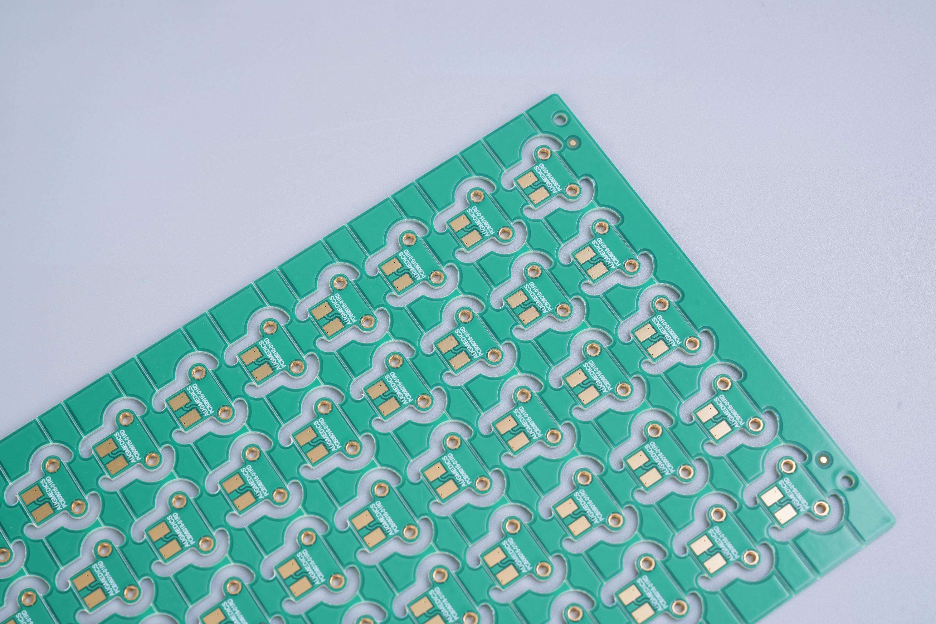
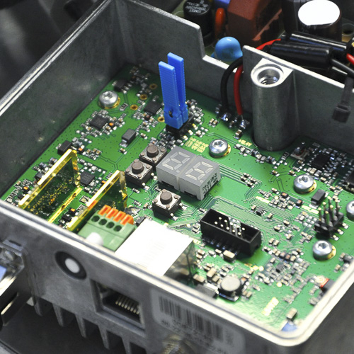
A PCBA board, however, is populated with electronic components. It may include ICs, connectors, resistors, sensors, and specialized chips. Once assembly occurs, the board gains a specific purpose, such as power regulation, communication, or control. Customs treats this assembly as a part of a machine or an electronic module.
Therefore:
- PCB = printed circuit (raw structure, no mounted parts)
- PCBA = module or part of a larger device (active, functional assembly)
Because the HTS system is function-based, PCBAs must be classified according to their function or application—not simply as “printed circuits.”
Can I Use Bare Board HS Code for PCBA Import & Export?
No, a bare board HS code cannot be used for a PCBA shipment. This is one of the most common mistakes made by buyers and new importers. Using HS 8534.00 for a populated PCBA is not acceptable in U.S. customs or in most global trade systems because:
- It misrepresents the product’s value.
- It misstates the function of the item.
- It leads to incorrect tariff calculation.
- It may trigger customs inspection or reclassification.
For example, a PCBA used in a communication product should fall under HS 8517.70. A PCBA used in an appliance belongs under a different heading. Filing it under HS 8534.00 would cause a mismatch between the invoice description and the actual product.
How to Find the Correct HTS Code for Your PCBA Board?
Selecting the correct HTS code for a PCBA requires a combination of technical understanding and compliance knowledge. Importers follow a structured approach to ensure the selected code is reasonable, accurate, and defensible during customs review.
Here is a practical method that companies use:
1. Define the function of the PCBA
Ask: What does the board do?
- Communication module
- Power control board
- Sensor or measurement board
- Industrial automation controller
- Automotive ECU board
This will point you to the correct HS chapter.
2. Look at the end product
What product does the PCBA support?
- A communication device → Chapter 85 (8517)
- A home appliance → Chapter 85 (various subheadings)
- A control instrument → Chapter 90 (9032)
The parent device determines the parent HTS number.
3. Check U.S. HTS database or your country’s HS system
The U.S. International Trade Commission (USITC) maintains updated HTS tables. Searching for the device type helps narrow down the code.

4. Review binding rulings
Customs rulings provide examples of how similar products were classified in the past. These rulings often help clarify classification for ambiguous cases.
5. Confirm with your customs broker
A licensed broker provides guidance aligned with import regulations. Many companies finalize their HTS selection with professional review to avoid risk.
6. Maintain consistency in documentation
The commercial invoice, packing list, CO, and airway bill must all reference the same HS number.
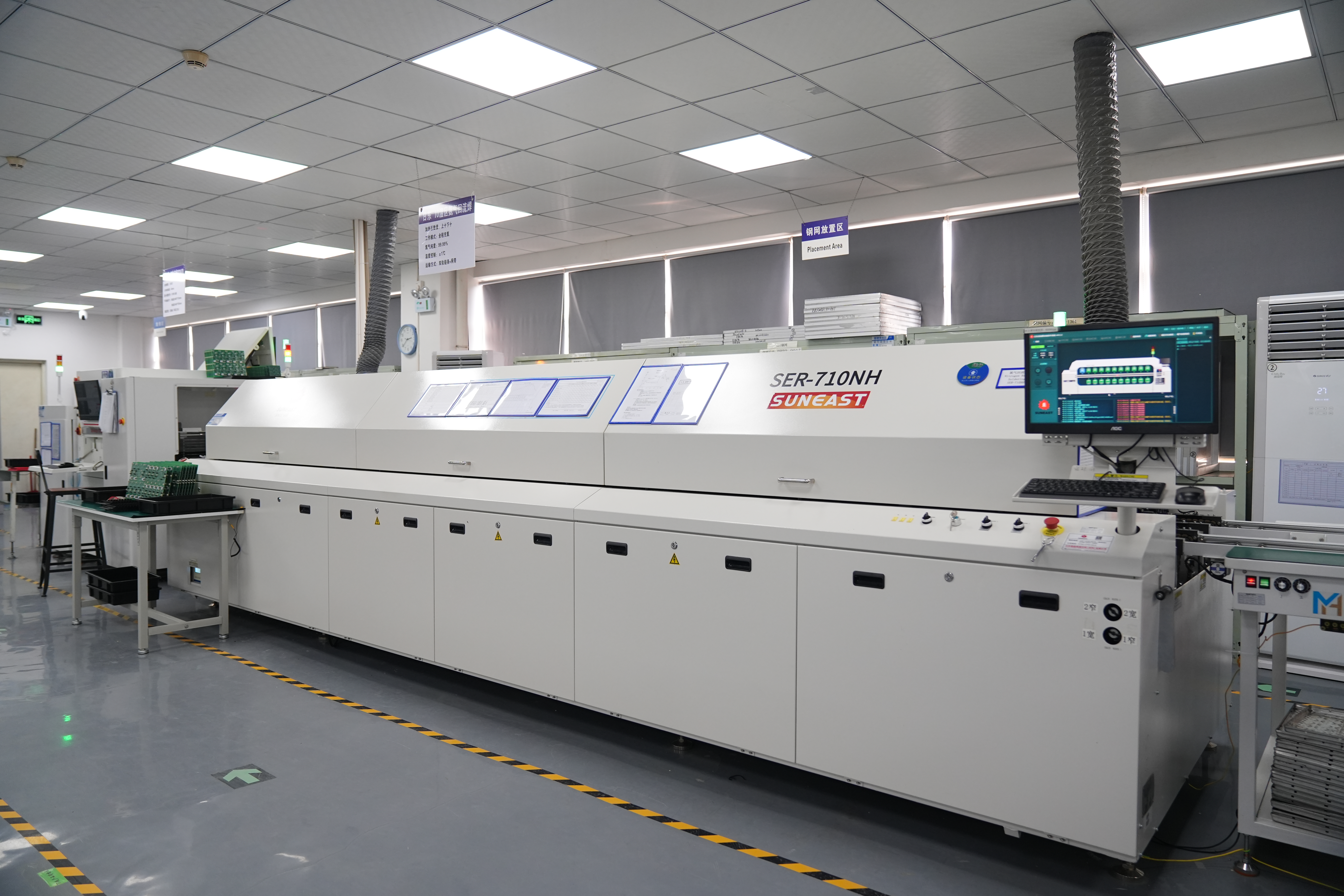
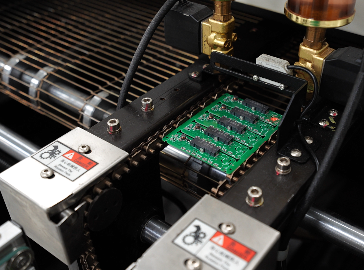
Why Work With EBest Circuit (Best Technology) for Global PCBA Shipments?
Companies looking for a reliable PCBA manufacturer benefit from working with a supplier who understands technical manufacturing and export procedures. EBest Circuit (Best Technology) supports customers across North America, Europe, and Asia with dependable engineering, stable production, and accurate shipment documentation.
EBest Circuit (Best Technology) offers:
- Professional PCB and PCBA manufacturing under ISO9001, ISO13485, IATF16949, and AS9100D
- Full traceability with MES systems
- Detailed export documents including recommended HTS codes
- Engineering support for prototype, low-volume, and mass-production PCBA
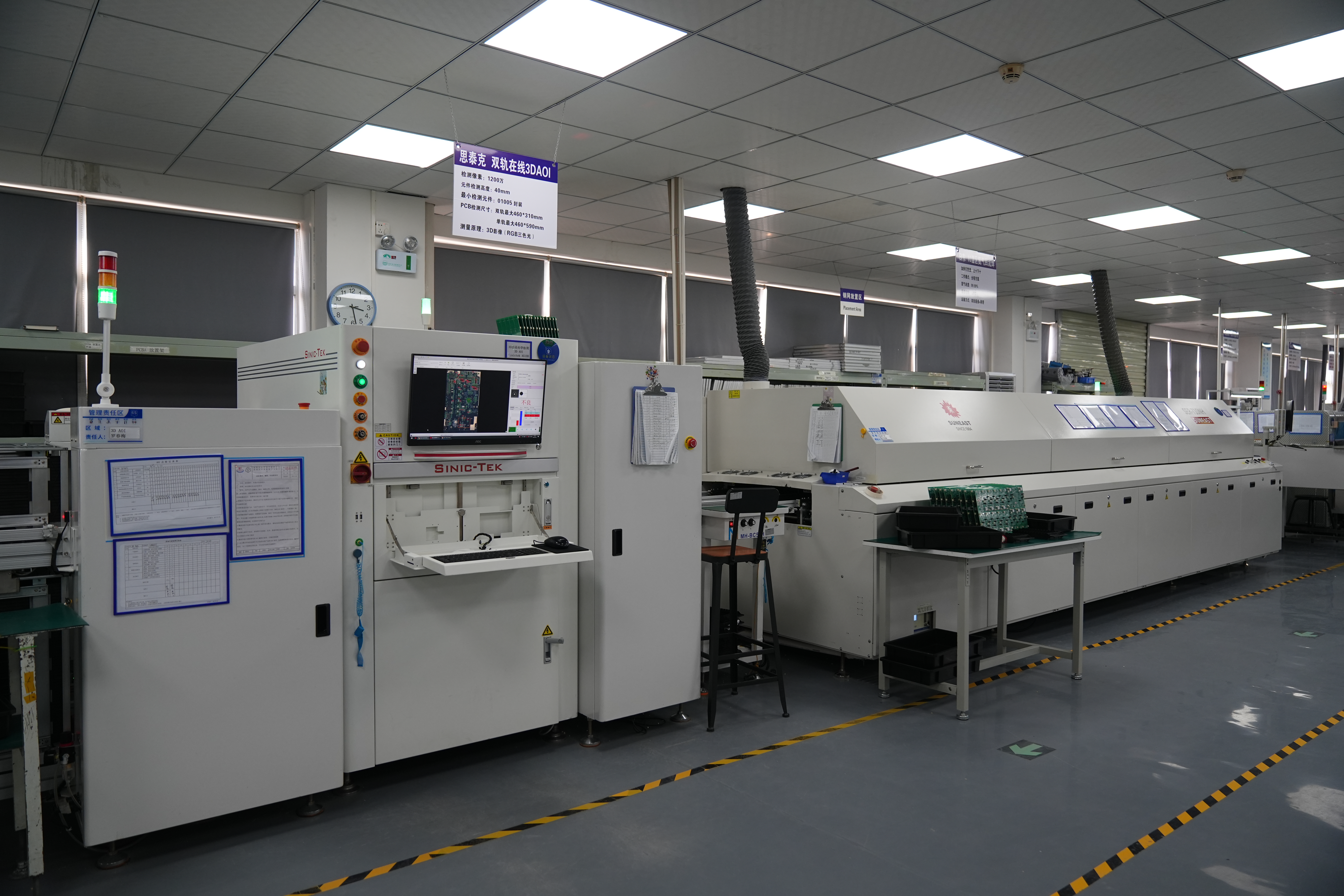
- High-mix capability covering RF boards, heavy copper boards, ceramic PCBs, HDI PCBs, and more
Accurate HTS classification is part of EBest Circuit (Best Technology)’s shipment workflow. With every order, customers receive consistent documentation that supports smoother customs clearance and reduced administrative work.
For PCBA projects requiring global shipping, EBest Circuit (Best Technology) helps simplify trade steps and shorten your delivery timeline.
Frequently Asked Questions
1. Is there a universal HTS code for all PCBA boards?
No. HTS codes for PCBA boards depend on their function and the device where they will be installed.
2. Can I classify a PCBA under HS 8534.00?
No. HS 8534.00 applies only to bare printed circuit boards without components.
3. Who decides the final HTS code: supplier or importer?
The importer has final responsibility for correct classification, although suppliers often provide recommendations.
4. Why does application matter so much for PCBA classification?
Because customs categorize PCBAs as “parts” of other devices. The parent device determines the correct HS code.
5. Can one PCBA have multiple possible HTS codes?
Yes. When a PCBA could belong to several categories, importers choose the most accurate code based on primary function.