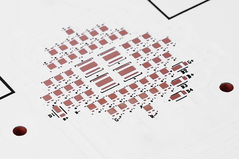
In high-power electronics, thermal management is everything. Whether you’re designing LED modules, motor controllers, or power converters, one of the first decisions you’ll make is selecting the right copper thickness for your copper core PCB.
It’s tempting to assume that more copper is always better. After all, thicker copper offers lower resistance and better heat conduction. But here’s the truth: while thicker copper can enhance performance, it also introduces new challenges—in cost, manufacturability, and even thermal efficiency in certain contexts.
In this article, we’ll dive into how copper thickness affects heat dissipation, mechanical integrity, and overall PCB performance. You’ll also learn how to find the sweet spot—balancing copper thickness with practical requirements.
What Does Copper Thickness Really Do in a PCB?
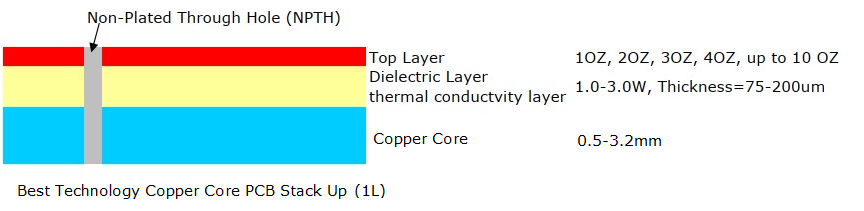
Copper thickness in a PCB is typically measured in ounces (oz), where 1 oz equates to approximately 35 micrometers of thickness. The thicker the copper, the more current it can carry and the more heat it can dissipate—up to a point.
For example:
- 1 oz copper is standard in many applications like consumer electronics or low-power LED boards.
- 2 oz–3 oz copper is often used in medium- to high-power applications, such as telecom equipment or automotive control modules.
- 4 oz–6 oz copper or more is reserved for ultra-high-current or extreme thermal environments, like industrial drives or inverters.
In a copper core PCB, the copper layer not only serves as a trace but also acts as a heat conduit. But simply adding more copper isn’t always the best strategy—it needs to be balanced with mechanical, thermal, and design constraints.
How Does Thicker Copper Affect Thermal Conductivity?
Thermal conductivity is the rate at which heat passes through a material. Copper’s thermal conductivity is excellent—about 398 W/m·K—much higher than FR4 (0.25 W/m·K) or aluminum (205 W/m·K). Thermal conductivity improves as copper gets thicker—up to a point.
- A 1 oz (35µm) copper layer offers good heat flow for standard loads.
- 2 oz (70µm) or 3 oz (105µm) copper layers are used for medium-to-high power circuits.
- Ultra-thick copper like 6 oz (210µm) or more is suitable for extreme applications like power inverters or motor drivers.
But while thicker copper improves thermal conductivity, it also increases thermal mass, which can slow down heat transfer in fast-cycling circuits. That means copper core PCBs with ultra-thick copper aren’t always the most efficient in dynamic thermal environments.
What Happens to Mechanical Strength as Copper Gets Thicker?
A copper core PCB with heavy copper also becomes more rigid. This can be beneficial in harsh environments (e.g. EV chargers, industrial robots) where vibration or mechanical shock is a concern.
However, ultra-thick copper comes with drawbacks:
- Reduced flexibility: Too much copper can crack during mechanical stress.
- Higher internal stress: Thicker copper can warp other layers if not carefully designed.
- Drilling and routing challenges: High copper thickness limits hole aspect ratio and increases the risk of burrs or tool breakage.
In short, thicker copper increases strength but decreases the PCB’s resilience during assembly or use.
Manufacturing Challenges of Thick Copper Core PCBs
As copper thickness increases, so does the cost—not just of materials, but also in processing:
- Etching Control: The deeper the copper, the harder it is to maintain precise trace widths and spacing. Over-etching or under-etching can occur, especially with high-aspect-ratio designs.
- Drilling Difficulties: Thick copper increases drill wear and may require specialized bits. This adds time and cost.
- Solder Mask Issues: Solder mask adhesion becomes less reliable with thick copper due to surface tension and lack of anchor points.
- Fine-pitch traces are harder to produce with heavy copper.
A copper core PCB with 3 oz copper may cost up to 1.8x more than a standard 1 oz version. And a 6 oz copper design might require specialized etching equipment, which not all PCB manufacturers can support. That’s why working with an experienced supplier like EBest Circuit (Best Technology) is crucial.
How to Choose the Right Copper Thickness for Your PCB?
Rather than defaulting to the thickest copper available, consider these design factors:
- Power Dissipation
Estimate total wattage and heat output. Use simulation tools or thermal imaging to understand hot zones.
- Current Capacity
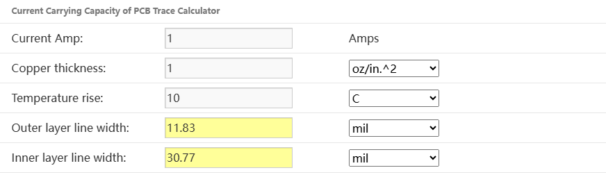
Follow IPC-2152 guidelines to determine trace width vs. amp load. For example:
1 oz copper: ~10A for 100 mil trace (surface)
2 oz copper: ~18A for same width
- Board Size and Layer Count
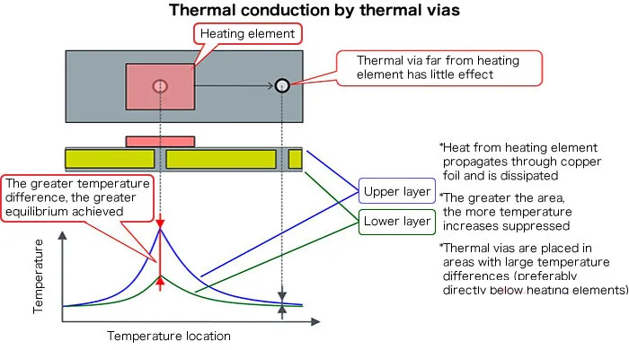
Larger boards may use thinner copper with thermal vias and heat sinks. Multilayer designs must balance all layers.
- Application Environment
Will the board be exposed to vibration, moisture, or rapid temperature swings? If yes, go thicker and stronger.
- Budget and Lead Time
Thick copper PCBs cost more and take longer to fabricate. Optimize design for performance within your price range.
Rule of thumb:
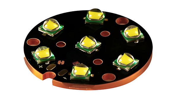
- Use 1 oz–2 oz copper for LED lighting, chargers, and automotive control boards.
- Go for 3 oz–4 oz only if you have continuous high current or extreme heat.
- Consider 5 oz+ only for industrial power systems or heavy-duty applications.
Case Study: How Thicker Copper Solved and Created Problems
A client building a 500W motor driver switched from 2 oz to 5 oz copper core PCB to improve thermal dissipation. While heat decreased by 12%, they faced new issues:
- Via drilling became inconsistent due to copper pull-out.
- Board warpage increased after reflow soldering.
- Assembly cost rose by 30%.
We helped them optimize with a hybrid solution:
- Kept 2 oz on signal layers.
- Added localized copper in power zones.
- Improved base layer contact for better heat flow.
Finally, thermal performance remained strong, but manufacturability and cost were brought back under control.
Conclusion
When designing a copper core PCB, it’s easy to fall into the trap of thinking “thicker is better.” In reality, optimal performance comes from careful engineering—not just stacking on copper.
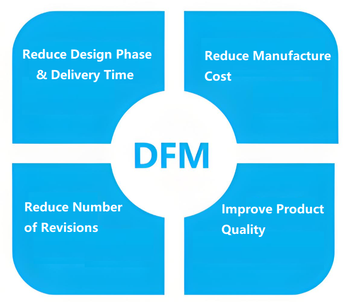
At EBest Circuit (Best Technology), we help clients worldwide balance copper thickness with thermal, mechanical, and manufacturing constraints. We use simulation, prototype validation, and DFM support to ensure your final product is both high-performing and cost-effective.
Why Work With EBest Circuit (Best Technology) for Copper Core PCBs?
We are not just PCB fabricators—we are problem solvers. Our copper core PCB services include:
✔️ Copper thickness options from 1 oz to 10 oz
✔️ Full-stack DFM analysis and thermal modeling
✔️ IPC-compliant thermal and electrical simulations
✔️ MES-based quality traceability
✔️ Rapid prototyping and scalable mass production
We help you avoid over-designing or under-designing copper thickness—saving cost and ensuring long-term reliability. No matter the application—EVs, LEDs, telecom, or industrial—you’ll find the right copper balance with us.
FAQs
Q1: Is 3 oz copper enough for a 100W LED module?
Yes, in most cases 3 oz copper on a properly designed copper core PCB can handle that heat load efficiently.
Q2: How does copper thickness affect signal integrity?
Thicker copper affects impedance. It must be calculated carefully for high-speed or RF circuits.
Q3: Can thick copper cause warping during reflow?
Yes. Uneven copper thickness across layers can cause thermal imbalance. This must be addressed in stack-up design.
Q4: What’s better: thicker copper or more thermal vias?
Depends. Thermal vias can be more efficient in some layouts and cost less than increasing copper.
Q5: Does EBest Circuit (Best Technology) support custom stack-ups for copper PCBs?
Absolutely. We provide custom stack-up planning based on your power, thermal, and mechanical needs.