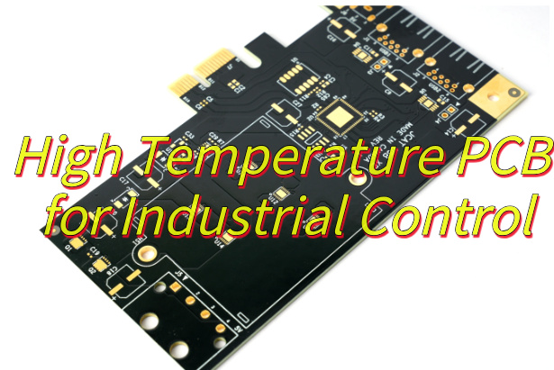
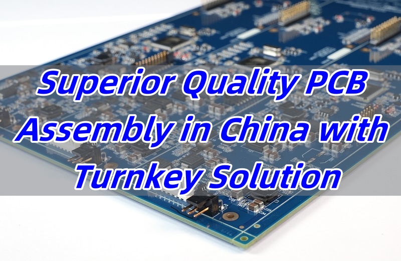
A DTP MCPCB, or Direct Thermal Path Metal Core PCB, also known sinkpad MCPCB, is a type of printed circuit board designed for high-power and high-heat applications. It helps electronics stay cool and stable, even under heavy loads. Compared to standard MCPCBs, DTP PCBs offer better thermal transfer and stronger mechanical support. Many industries, including LED, power supply, automotive, and telecom, now prefer DTP copper MCPCBs for reliable performance.
In this blog, we’ll explain what DTP means, its features, structure, design tips, manufacturing process, and how it fits into modern electronics.
What Is DTP and Its Features?
DTP stands for Direct Thermal Path. It refers to a design where heat moves directly from hot components to the metal base without many thermal barriers. This path lowers thermal resistance and keeps components cooler.
Main Features of DTP:
- Direct connection between heat source and metal base
- Higher heat dissipation than traditional MCPCBs
- Stronger thermal conductivity through thick copper or copper convexity
- Better reliability in high-power circuits
- Long-lasting even under thermal cycling and vibration
This structure reduces the chance of overheating, which helps the whole system run longer and safer.
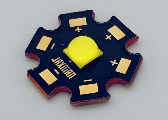
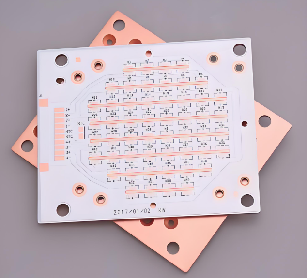
DTP Copper MCPCB Structure
A DTP copper MCPCB uses a raised copper structure (called a copper convexity or copper boss) formed directly on the metal base. This convex feature aligns under the heat source, typically a power component like a MOSFET or high-wattage LED. The DTP copper PCB layers are:
- Top Layer: Copper trace for electrical routing
- Dielectric Layer: High thermal conductivity insulation
- Copper Convexity: Directly contacts both the component and the base
- Metal Base: Usually aluminum or copper for heat spreading
Its stackup layers is:
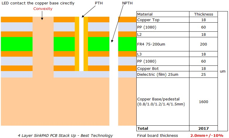
This design bypasses traditional insulation layers and allows heat to flow directly into the metal core.
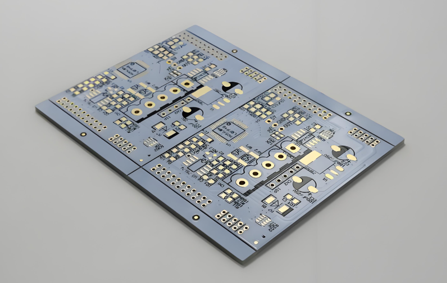
DTP MCPCB vs Traditional MCPCB
Standard MCPCBs have a thin dielectric layer between the copper trace and the metal base. This layer adds thermal resistance. In contrast, a DTP PCB reduces this resistance by forming a direct path between the component and the base metal using copper convexities.
| Feature | DTP MCPCB | Traditional MCPCB |
| Heat Transfer | Direct (through copper convexity) | Through dielectric |
| Thermal Resistance | Very Low | Medium |
| Use Case | High-power, LED, EV, power supply | General LED, moderate power |
| Cost | Higher | Lower |
| Performance | Excellent | Good |
Where Are DTP PCBs Used?
DTP MCPCBs are perfect for any application where heat is a big issue. They’re now standard in many thermal-critical products. The main applications including:
- High-power LED lighting
- Power supplies and inverters
- Electric vehicles (EVs) and battery packs
- RF and telecom base stations
- Solar energy systems
- Laser modules and sensors
Whenever components get hot and space is tight, DTP copper MCPCBs offer a smart solution.
Tips for MCPCB Design with DTP Structure
Designing a DTP PCB requires special attention to thermal paths, layout, and material selection.
- Place heat-generating components directly over copper convexities
- Use high-conductivity dielectric materials to keep thermal resistance low
- Align thermal vias with component pads for effective heat flow
- Choose a suitable base material: aluminum for cost, copper for performance
- Ensure planarity and flatness for solid thermal contact
A carefully designed DTP MCPCB handles more power without compromising safety or reliability.
Why Is the Price of DTP MCPCB Higher Than a Normal MCPCB?
The cost of a DTP MCPCB is higher due to the complexity of its design and processing. It uses thicker copper or custom copper convexities, which are more expensive than standard copper foil. Creating a precise raised copper feature under each heat source requires extra machining steps, tight alignment, and rigorous quality checks.
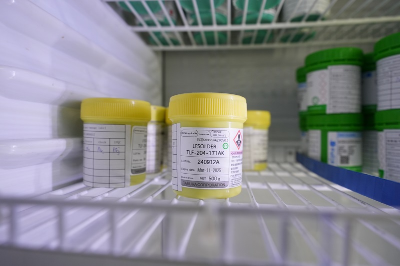
Additionally, the dielectric materials used must have very high thermal conductivity and are usually more costly. The manufacturing process also involves advanced methods like X-ray alignment, CNC machining, and thermal performance testing. Despite the higher price, DTP MCPCBs offer long-term savings by improving thermal efficiency, reducing failure rates, and extending product lifespan.
How DTP MCPCBs Are Manufactured?
The manufacturing of a DTP MCPCB is more advanced than a standard MCPCB manufacturing process. It focuses on forming a raised copper boss (convexity) that provides a one-piece thermal bridge between the heat source and the metal base.
1. Base Metal Preparation
The aluminum or copper base is cleaned and pre-treated. This forms the foundation for the entire board.
2. Creating the Copper Convexity
A raised copper feature is formed on the base metal. This copper boss is placed directly beneath high-heat components. The convexity may be CNC machined or created during the copper plating process.
3. Dielectric Layer Lamination
A thin, high-thermal-conductivity dielectric is laminated around the copper convexity and onto the metal base. The copper bump remains exposed to make direct contact with the top copper circuit.
4. Copper Foil Application & Circuit Etching
Copper foil is laminated onto the surface and patterned using photolithography. The exposed part of the copper boss connects directly to a pad on the top layer.
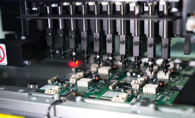
5. Drilling & Plating (if required)
If the design includes signal vias or multi-layer connections, micro-drilling and copper plating are applied carefully to avoid damaging the copper boss.
6. Solder Mask & Surface Finish
Solder mask is printed, leaving heat transfer pads exposed. Surface finish (e.g., ENIG, HASL) is applied for soldering protection.
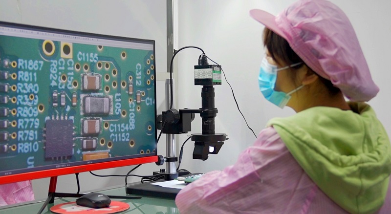
7. Inspection & Testing
- X-ray confirms alignment of copper convexity under the pad
- Thermal resistance is measured
- Electrical continuity is tested
- Visual and mechanical checks ensure no delamination or defects
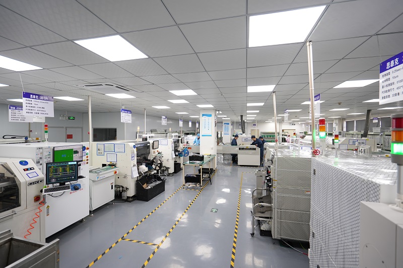
This process requires tight process control and high-end fabrication equipment.
Benefits of Using DTP Copper MCPCB in High-Power Electronics
- Superior thermal performance for high-wattage components
- Longer component life due to reduced junction temperatures
- Smaller form factor with higher power density
- Stable performance under vibration, shock, and thermal cycling
- Improved system efficiency and lower cooling requirements
These benefits make DTP MCPCBs an excellent investment for demanding applications.
DTP PCB Material Choices
A high-quality DTP PCB relies on the right materials:
- Copper Convexity: Pure copper, usually 1–4mm thick
- Dielectric Layer: Ceramic-filled epoxy or other high-conductivity material
Metal Base:
- Aluminum: Lightweight, good for general use
- Copper: Best thermal conductivity, ideal for extreme conditions
The right combination depends on your project needs, thermal limits, and cost targets.
Why Work With a Reliable DTP MCPCB Manufacturer?
Not all PCB manufacturers can build DTP MCPCBs. You need a supplier with tight process control, CNC machining, and advanced lamination tools.
A good DTP supplier should offer:
- Custom DTP MCPCB design support
- In-house thermal simulation and analysis
- CNC or stamping for copper convexity
- X-ray and AOI for high-precision quality control
- Quick prototyping and scalable volume production
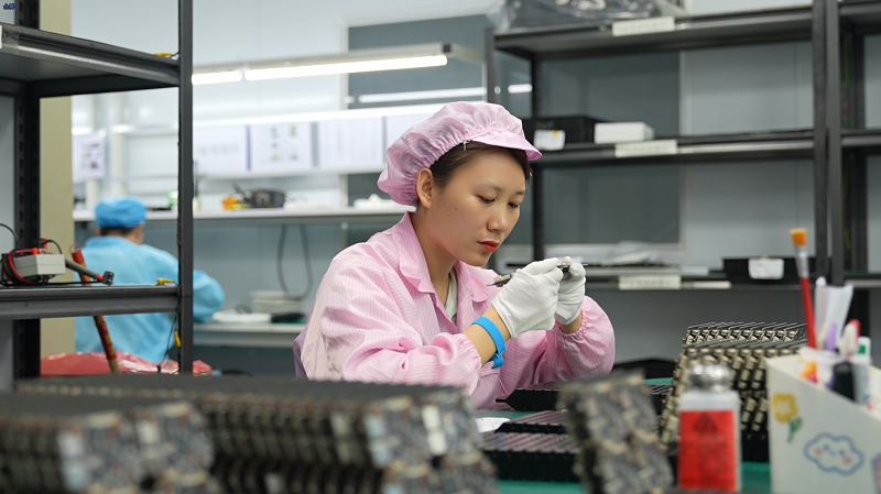
About EBest Circuit (Best Technology)
At EBest Circuit (Best Technology), we are experts in DTP MCPCBs, aluminum PCBs, and thermal solution boards. We serve industries including LED, automotive, telecom, and medical electronics. We also use MES systems to provide full traceability of materials and processes. Our team can support you from design to mass production with reliable engineering and fast service.
FAQs
1. What is a DTP MCPCB?
A Direct Thermal Path MCPCB uses a raised copper convexity to transfer heat directly from the component to the metal base.
2. How does a DTP copper MCPCB differ from a standard one?
It bypasses insulating layers by forming a direct copper path, reducing thermal resistance.
3. What are the main uses of DTP PCBs?
Used in LED lighting, power supplies, automotive electronics, and telecom base stations.
4. Why is the DTP MCPCB more expensive?
It uses more copper, complex machining, high-end materials, and tighter quality control.
5. Does EBest Circuit (Best Technology) offer custom DTP MCPCB services?
Yes, we provide full engineering support, fast prototyping, and scalable production.