If you’ve come across the term CPR on a PCB, you might be wondering what it means. While it’s not as commonly known as terms like VCC or GND, CPR plays an important role in many circuit designs. Depending on the context, CPR can have different meanings. In this blog, we’ll explore the meaning of CPR on a PCB, its typical applications, and how it impacts circuit performance.

What Does CPR Stand for on a PCB?
On a PCB, CPR most commonly stands for Current Path Resistor. This component is used to control or monitor the flow of current through specific parts of a circuit. It can help protect sensitive components by limiting the current or providing a voltage drop where needed.
In some cases, CPR might also stand for:
- Charge Pump Resistor – In voltage conversion circuits, a CPR is used to manage the charge and discharge cycles of capacitors like DC-DC converters. This is mainly used to ensure efficient voltage boosting or regulation
- Component Placement Reference – In some PCB designs, CPR may simply be a reference label used to identify a specific resistor during assembly or testing.
What is a Current Path Resistor (CPR)?
A Current Path Resistor is a resistor placed strategically in a circuit to control the flow of current. It acts as a safeguard by limiting the current that can pass through, protecting downstream components from damage due to excessive current.
Functions of a Current Path Resistor:
- Current Limiting: By introducing resistance, the CPR ensures that the current stays within safe limits, preventing overcurrent damage.
- Voltage Division: It can create a voltage drop that is proportional to the current, which is useful in voltage division circuits.
- Current Sensing: In some applications, the voltage drop across the CPR is measured to monitor or control the current flow in real-time.
For example, in LED circuits, a CPR is often used to limit the current flowing through the LEDs, ensuring they operate within their rated specifications.
How Does a Current Path Resistor Work?
A current path resistor works by offering resistance to the current flowing through a specific circuit path. By doing so, it limits the current to a safe level for downstream components.
For example, in power distribution circuits, the CPR helps:
- Prevent excessive current from damaging components.
- Maintain consistent current levels across multiple branches of the circuit.
- Provide a measurable voltage drop that can be used for current sensing.
Current path resistor is an important component in power management and protection circuits.
How to Identify CPR on a PCB?
Identifying the CPR on a PCB can be straightforward if you know where to look. Here are some tips:
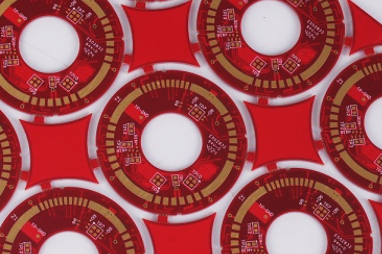
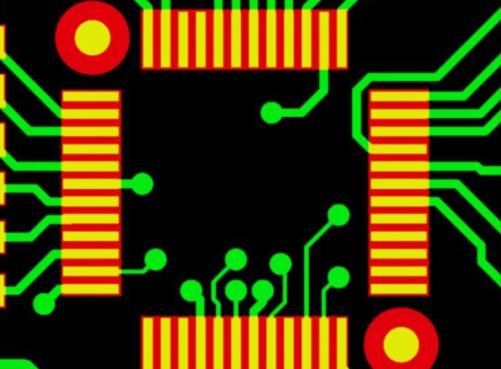
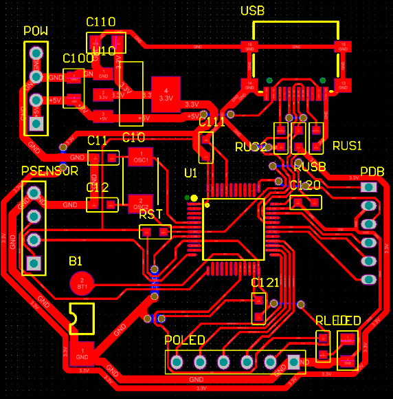
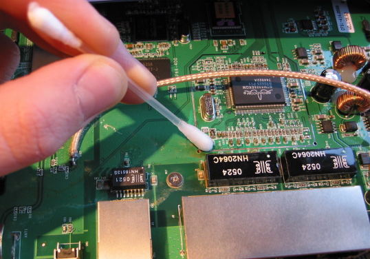
1. Check the Silkscreen: Most PCBs have a silkscreen layer that labels components with their designators. Look for labels like CPR, R, or specific numbers (e.g., R15) near resistors.
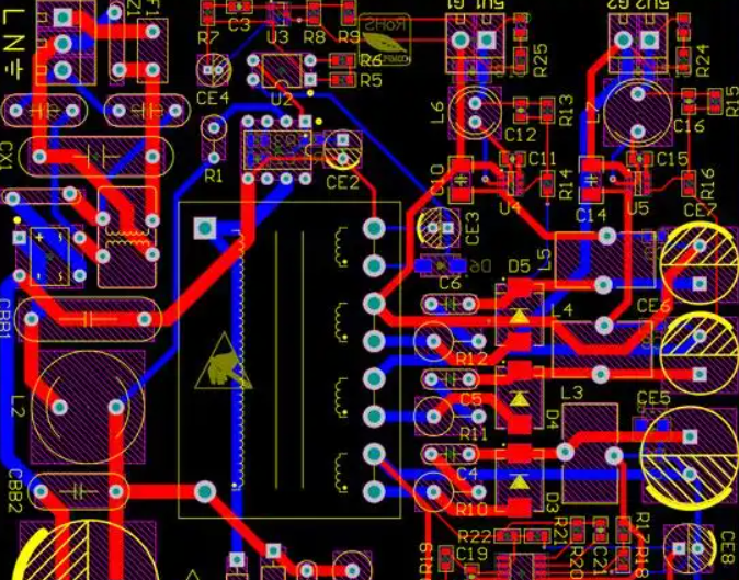
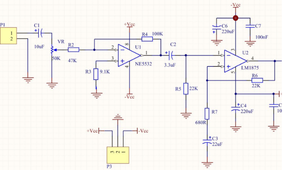
2. Refer to the Schematic: The circuit schematic provides detailed information about the components, including their placement and function.
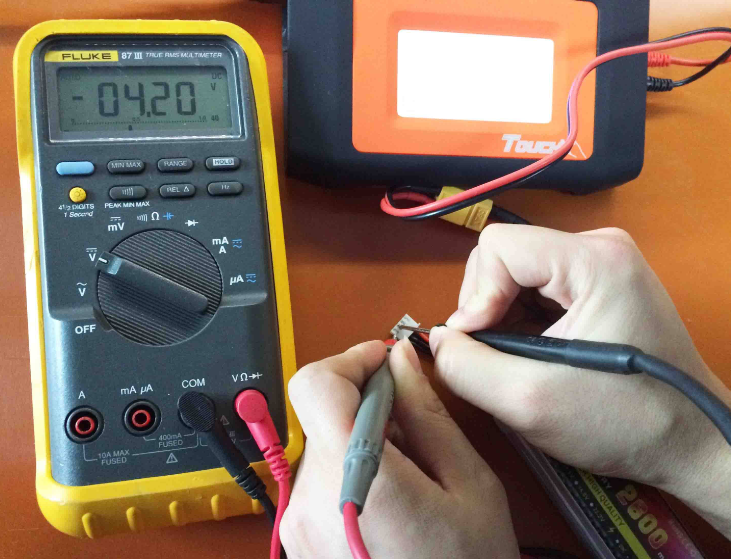
3. Use a Multimeter: If you suspect a resistor is the CPR but it’s not labeled, you can use a multimeter to measure its resistance and compare it with the schematic values.
4. Look for Nearby Components: CPRs are often placed near components they protect or control, such as LEDs, capacitors, or ICs.
Common Applications of CPR in Electronics
CPRs are used in a variety of applications across different types of electronic devices. Their ability to control current and voltage makes them essential in many circuit designs, including:
- Power Management Circuits
CPRs help manage the distribution of power across different sections of a circuit, ensuring that each section receives the correct amount of current.
- Current Sensing Modules
In current sensing circuits, the voltage drop across the CPR is measured to determine the current flowing through the circuit. This information can be used for monitoring or control purposes.
- Overcurrent Protection
CPRs are often used in protection circuits to prevent overcurrent conditions from damaging sensitive components.
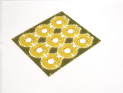
- LED Lighting Systems
In LED circuits, CPRs limit the current flowing through the LEDs, preventing them from burning out and ensuring consistent brightness.
- Voltage Conversion Circuits
Charge pump circuits, which require precise timing and current control, rely on CPRs to maintain stable and efficient operation.
How to Choose the Right CPR for Your Circuit?
Selecting the right CPR for your circuit is crucial for ensuring optimal performance and reliability. Here are some factors to consider:
- Resistance Value: Choose a resistor with the appropriate resistance value to achieve the desired current limit or voltage drop.
- Power Rating: Ensure the resistor can handle the power dissipation without overheating or failing.
- Tolerance: Select a resistor with a tight tolerance if precise current control is required.
- Temperature Coefficient: Consider the resistor’s temperature coefficient if the circuit will operate in varying temperature conditions.
The term CPR on a PCB might not be as widely recognized as other designations, but it plays a significant role in circuit performance and reliability. Whether it stands for Current Path Resistor or other terms, understanding its function can help you design better circuits and troubleshoot issues more effectively.
At EBest Circuit (Best Technology), we specialize in providing high-quality PCBs tailored to your specific needs. From design to manufacturing, our team ensures that every component, including CPRs, is optimized for performance and reliability. Contact us today to learn how we can help with your next project.