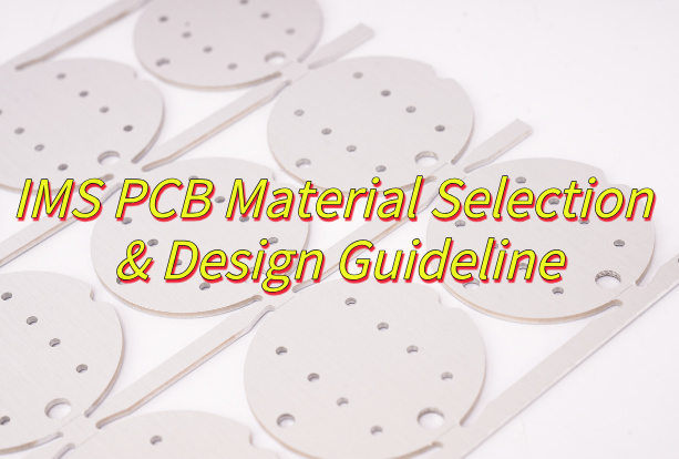
How to calculate thermal resistance of aluminum PCB? This guide explains aluminum PCB thermal resistance fundamentals, selection criteria, calculation methods, influencing factors, design optimization techniques, and testing procedures for efficient thermal management.
Are you troubled these issues?
- Does your LED lamp accelerate the light decay due to insufficient heat dissipation?
- How to solve the frequent overheat protection of high-power power modules?
- How to ensure batch stability due to large fluctuations in thermal resistance of traditional FR4 boards?
EBest Circuit (Best Technology) Can Provide:
- Precise customization: 0.8-5.0°C/W thermal resistance aluminum substrate ±5% tolerance control, matching your thermal design critical value.
- Data endorsement: JEDEC standard thermal resistance test report is provided for each batch.
- Scenario design: 1.2mm ultra-thin heat spreader/multi-layer stacking structure, actual measurement reduces the temperature of key nodes by 20℃.
Feel free to contact us now if you have any inquiry for aluminum PCB: sales@bestpcbs.com.
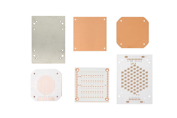
What Is the Thermal Resistance of Aluminum PCB?
The thermal resistance of an aluminum PCB typically ranges from 0.5 to 3.0°C/W, depending on its construction. Key factors include the thickness of the dielectric layer (50–200μm), the thermal conductivity of the aluminum base (160–200W/m·K), and the copper circuitry layout. Compared to FR4 PCBs (10–20°C/W), aluminum substrates offer 5–10× better heat dissipation due to their superior thermal conductivity. For high-power applications, designs with ceramic-filled dielectrics or hybrid materials can achieve thermal resistances below 0.2°C/W. Performance varies with aluminum alloy type (e.g., 6061 vs. 1060) and surface treatments like anodizing.
How to Choose the Thermal Resistance Type of Aluminum PCB?
Aluminum PCB Thermal Resistance Type Selection Guide:
1. Prioritize power requirements by thermal resistance value
- Low thermal resistance type (<0.5℃/W): Suitable for high power density scenarios (such as LED modules >5W/cm², electric vehicle power modules). Although the unit price is high, it can reduce the junction temperature by more than 40℃, significantly extending the life of the device.
- Medium thermal resistance type (0.5-1℃/W): Used for medium power equipment (such as household appliance power supplies, industrial controllers), balance heat dissipation performance and cost, and the thickness of the insulation layer is usually controlled at 80-100μm.
2. Optimize cost performance by structural selection
- Traditional FR-4 composite type: Select when only basic heat dissipation is required (such as low-power LED light strips), the cost is 40%-60% lower than that of dedicated aluminum substrates, but the thermal resistance is >1℃/W.
- Magnetic control sputtering technology type: Suitable for high-frequency and high-temperature applications (such as 5G base station RF modules), the insulation layer is thinner (50-75μm), and the thermal resistance is as low as 0.1℃/W, but the process cost increases by 20%-30%.
- Multilayer thermal conductive structure type: The first choice for complex systems (such as server power supplies). The hot spots are dispersed through multi-layer thermal conductive dielectrics. The thermal resistance can be controlled at 0.3-0.8℃/W, which is suitable for multi-chip integrated design.
3. Cost-sensitive alternatives
- Hybrid design: Aluminum substrate is used for the core high-heat area (such as the CPU cooling area), and FR-4 is used for the peripheral circuit, which reduces the overall cost by 25%-40%.
- Copper foil thickness optimization: 1oz copper foil meets most scenarios, and 3oz copper foil (105μm) is only used for ultra-high current to avoid excessive design and increase board costs.
Tips: First determine the allowable temperature rise through thermal simulation, and then compare the thermal resistance-price curves of different models, and give priority to the lowest cost solution that meets the temperature control requirements.
How to Calculate Thermal Resistance of Aluminum PCB?
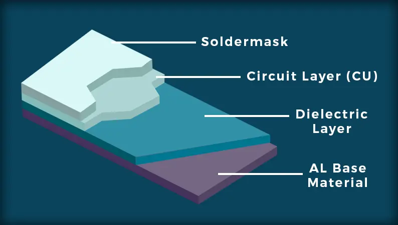
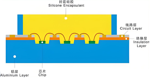
The thermal resistance (Rθ) of aluminum PCBs is calculated by combining material and structural parameters: Rθ = (L₁/(k₁·A₁)) + (L₂/(k₂·A₂))
- L: Thickness of each layer (meters)
- k: Thermal conductivity (W/(m·K))
- A: Heat dissipation area (square meters)
The aluminum substrate layer (k₁≈1-5 W/(m·K)) and insulating layer (k₂≈0.5-3 W/(m·K)) contribute additively to thermal resistance, while the copper layer’s resistance is typically negligible. Ensure unit consistency and account for the series relationship of heat dissipation paths in practical calculations.
What Factors Affect the Thermal Resistance of Aluminum Substrate?
- Material Thermal Conductivity — Lower conductivity in the dielectric layer increases thermal resistance due to reduced heat transfer efficiency.
- Layer Thickness — Thicker dielectric layers raise resistance, while thinner aluminum bases may limit heat spreading capabilities.
- Interface Quality — Poor contact surfaces between aluminum and dielectric layers add interfacial thermal resistance, impacting overall performance.
- Structural Elements — Features like thermal vias or hybrid composites (e.g., with carbon nanotubes) enhance heat dissipation and lower resistance.
- Environmental Factors — Moisture absorption and high operating temperatures degrade thermal properties, increasing resistance in humid or extreme conditions.
- Surface Treatments and Coatings — Protective or conductive finishes alter heat flow, reducing resistance if optimized for thermal management.
- Density and Porosity — Higher density dielectric materials improve insulation but may increase resistance, whereas porosity can trap air and worsen performance.
How to Design to Reduce the Thermal Resistance of Aluminum PCB?
Design Strategies to Reduce Aluminum PCB Thermal Resistance:
- Optimize Dielectric Layer: Use thinner, high-thermal-conductivity insulation (e.g., graphene-filled or ceramic-filled prepreg) to reduce heat transfer barriers.
- Increase Metal Core Thickness: Thicker aluminum substrates (e.g., 2.0mm vs. 1.0mm) enhance lateral heat spreading.
- Maximize Copper Coverage: Use thicker copper traces (≥2oz) and expand ground/power planes to boost heat dissipation.
- Add Thermal Vias: Place arrays of small, closely spaced vias under high-power components to channel heat to the aluminum layer.
- Improve Component Layout: Position heat-generating parts centrally over the aluminum core and avoid clustering.
- Select Low-Thermal-Resistance Materials: Choose aluminum alloys (e.g., 6061-T6) with higher thermal conductivity (≈167 W/m·K).
- Incorporate Heat Sinks: Attach external heat sinks or vapor chambers to the PCB’s aluminum surface for forced convection.
- Use Thermal Interface Materials (TIMs): Apply high-conductivity TIMs (e.g., thermal grease, phase-change pads) between components and the PCB.
- Simulate Early: Utilize thermal simulation tools (e.g., ANSYS Icepak) during design to identify and mitigate hotspots.
- Minimize Insulation Layer Count: Reduce multilayer stacking; opt for single-sided aluminum PCBs where feasible.
How to Test the Thermal Resistance of Aluminum PCB?
1. Sample Preparation
- Clean aluminum substrate surface oxidation layer with alcohol and dry thoroughly.
- Apply thermal grease uniformly on the test area (thickness ≤0.1mm).
- Securely mount heating components (e.g., power resistors) at the center of the test point.
2. Steady-State Method (Standard Procedure)
- Reference standard: IPC-TM-650 2.6.7.2
- Apply constant power (recommended 1-5W/cm²) until thermal equilibrium (±1℃/min temperature change).
- Simultaneously measure temperatures with K-type thermocouples:
- T1: Heating element surface temperature.
- T2: Aluminum substrate backside temperature (3cm from test point).
- T3: Ambient temperature (20cm from sample).
- Calculate thermal resistance: Rθ = (T1-T2)/Power.
3. Transient Method
- Reference standard: ASTM D5470 variant
- Apply square-wave power (duty cycle ≤10%).
- Capture temperature curves at high speed (≥100Hz).
- Derive thermal resistance via exponential fitting: Rθ = (T_max-T_ambient)/Power
4. Thermal Imaging Verification
- Use a calibrated infrared thermal imager (accuracy ±2℃).
- Capture steady-state temperature distribution maps.
- Validate hotspot locations against theoretical heat flow paths.
5. Environmental Control Requirements
- Temperature: 25±1℃ (forced air cooling requires airflow velocity ≤1m/s).
- Humidity: 45±5%RH.
- Chamber volume ≥1m³ to minimize boundary effects.
6. Data Processing Standards
- Average results from ≥3 repeated tests.
- Maximum allowable deviation: ±5% for steady-state method, ±8% for transient method.
- Exclude abnormal data from nonlinear temperature rise phases.
7. Special Notes
- For aluminum substrates with thickness ≥1.5mm, additional lateral thermal resistance testing is recommended. Multipoint temperature measurements should be conducted to evaluate thermal diffusion performance.
- The test report must include thermal resistance values, testing conditions, equipment accuracy specifications, and thermal imaging attachments.
Why Choose EBest Circuit (Best Technology) as Aluminum PCB Manufacturer?
- Precision Thermal Resistance Control: Provide customized thermal resistance values (0.8-5.0°C/W) with ±5% tolerance, ensuring predictable thermal performance for your designs. It can reduce thermal design margins and optimized system costs.
- Thermal Performance Verification: Every PCB undergoes JEDEC-standard thermal testing with detailed reports, giving clients certified performance data for reliability compliance.
- Application-Specific Thermal Solutions: Tailored designs (e.g., 1.2mm thick for LEDs, multilayer for power modules) lower operating temperatures by 15-20°C. It can achieve longer product lifespan and reduced heatsink costs without redesigns.
- 24-hour rapid prototyping: shorten the R&D cycle by 50% and accelerate product launch
- Competitive & Transparent Pricing – No hidden costs, offering the best value without compromising quality.
- Turnkey Solutions – Full-service PCB manufacturing from design to delivery, accelerating your product’s time-to-market.
- ISO 14001/ISO 13485 certification: medical/automotive customers are exempt from secondary testing, and compliance costs are reduced by 30%.
- Free DFM (Design for Manufacturability) Analysis: Optimizes PCB layouts to reduce material waste, lower production costs, and avoid late-stage design revisions.
Welcome to contact us if you have any request for aluminum PCB: sales@bestpcbs.com. Looking forward to hearing from you soon!