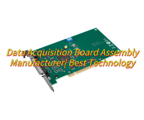
What is a data acquisition board? Let’s discover its components, working principle, function, application, build process, how to connect Arduino to data acquisition board.
Are you troubled with the following questions?
- Signal crosstalk degrading sampling accuracy, forcing costly shielding?
- MOQ blocking rapid prototyping, causing inventory buildup?
- Multi-channel timing drift traced to PCB layout, not algorithms?
As a data acquisition board assembly manufacturer, EBest Circuit (Best Technology) can provide you solutions:
- Signal Integrity: 4-layer hybrid stack with isolated analog channels, boosts ADC SNR ≥85dB, cuts BOM costs by 15%.
- Flexible Production: 10-piece MOQ, 24-hour line-switch, 72-hour delivery (files to finished boards).
- Pre-DFM Validation: Free layout review to preempt 17 timing issues, locks ≥98.5% first-pass yield (2025 Q2 verified).
Welcome to contact us if you have any request for data acquisition board assembly: sales@bestpcbs.com.
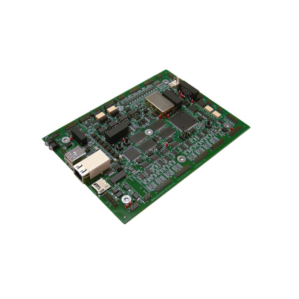
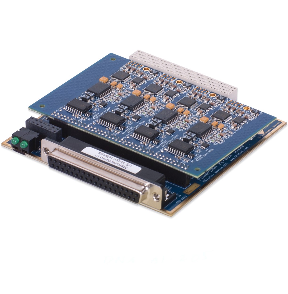
What Is a Data Acquisition Board?
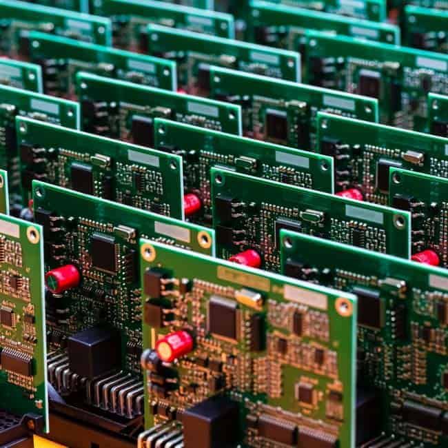
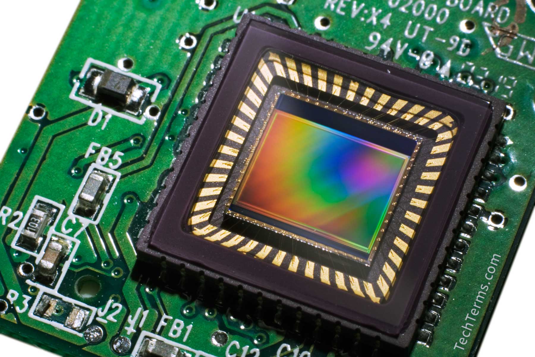
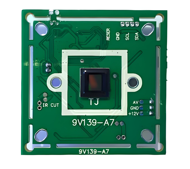
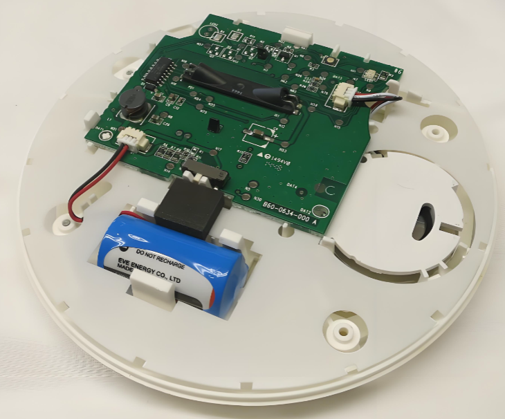
The Data Acquisition Board (also called as DAQ Board), as the core hardware component of the Data Acquisition System (DAQ), is responsible for converting real-world analog signals (such as temperature, pressure, voltage, etc.) into digital signals through Analog-to-Digital Converters (ADCs), enabling computers to process and analyze them.
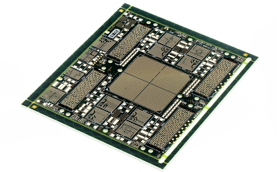
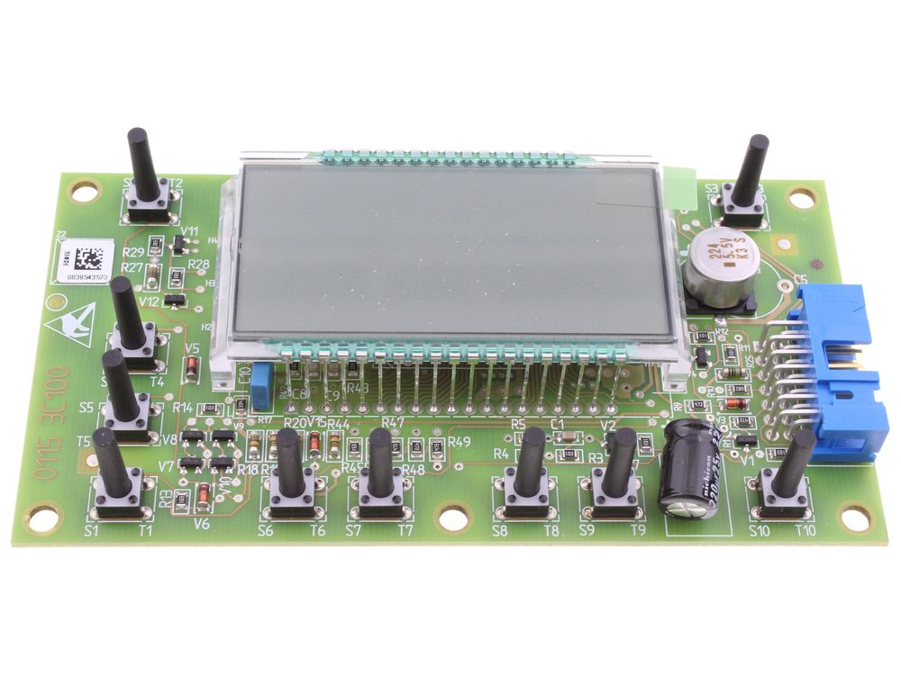
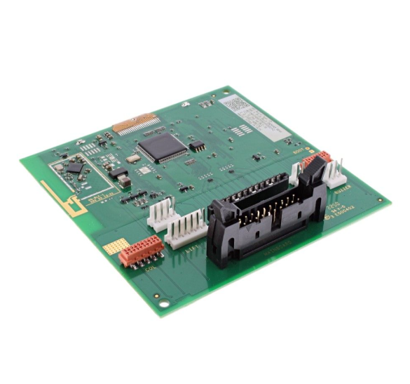
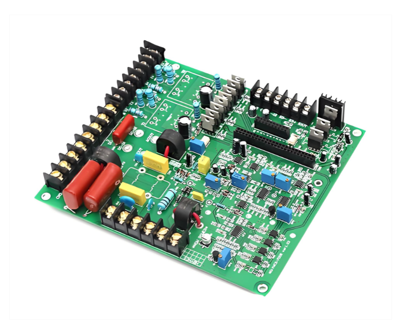
Components of Data Acquisition Board
- Analog Front End: Receives raw analog signals.
- Multi-channel ADC: Enables high-precision signal conversion with support for multi-channel simultaneous sampling.
- FPGA (Field-Programmable Gate Array): Generates interrupt signals to trigger ADCs, ensuring precise timing synchronization.
- Processor (e.g., ARM Cortex-M3): Handles digital data processing and manages communication protocols.
- High-Speed Bus: Links the processor to ADCs, optimizing data transmission efficiency for real-time processing.
How Does a Data Acquisition Board Work?
Data Acquisition Board (DAQ) Working Principle:
- Signal Input & Conditioning: Sensor signals (e.g., voltage, current, temperature) enter the DAQ board via input terminals. Conditioning circuits amplify, filter, or isolate raw signals to match the ADC’s input range (e.g., ±10V), ensuring optimal signal quality for conversion.
- Analog-to-Digital Conversion (ADC): Conditioned analog signals are digitized by the ADC, typically with 12–24-bit resolution. Sampling rates range from kS/s to GS/s, tailored to applications—e.g., ≥44.1 kS/s for audio capture.
- Clock Synchronization & Triggering: A high-precision clock (e.g., TCXO/PLL) governs sampling timing, achieving multi-channel synchronization errors <1μs. Hardware/software triggers (e.g., external pulse) precisely start/stop acquisition.
- Data Processing & Buffering: FPGA/MCU performs real-time processing (e.g., digital filtering, FFT analysis). DMA transfers data to onboard memory (e.g., DDR4), preventing loss due to PC latency.
- Data Transmission: Processed data is uploaded to the host via high-speed interfaces (PCIe, USB 3.0, Ethernet). Bandwidth must align with sampling rates, such as 16 Mbps minimum for 1 MS/s 16-bit data.
What Is the Function of the DAQ Board?
- Multichannel Data Acquisition: Enable simultaneous sampling of multiple signal sources for efficiency; e.g., 16-bit 5-channel data acquisition board handle multi-channel analog inputs for complex system monitoring.
- High-Precision Signal Conversion: Utilize high-resolution ADCs (12/16-bit) for accurate analog-to-digital conversion, minimizing quantization errors. Medical imaging systems employ 12-bit ADCs to ensure data fidelity.
- Real-Time Data Processing & Control: Integrate processors (ARM Cortex-M3, FPGA, DSP) for real-time algorithm execution and feedback control. ARM-FPGA collaboration generates interrupts and processes sensor data for dynamic system control (e.g., Stewart Platform motion control).
- Data Storage & High-Speed Transfer: Include buffers (registers) and high-speed interfaces (USB, optical fiber, PCIe) for efficient data handling. PCIe40 boards use fiber optics for large-data throughput; USB interfaces simplify server connectivity.
- System Monitoring & Diagnostics: Feature status indicators (LEDs) and diagnostic tools for fault detection. LEDs provide visual status feedback, enhancing maintainability.
- Programmability & Flexibility: Leverage FPGA/microcontroller-based architectures for software-defined customization. FPGA platforms allow user-defined logic for adaptable control (e.g., signal processing, system tuning).
What Are Applications of DAQ Board?
- Industrial control: Real-time temperature, pressure, and vibration acquisition on production lines, closed-loop process optimization.
- Scientific measurement: Nano-displacement high-speed pulse capture, precision analysis of bioelectric signals (EEG/EMG).
- Medical monitoring: Digitization of physiological signals (ECG/blood oxygen), continuous monitoring of vital signs in the ICU.
- Environmental monitoring: Wind speed and humidity data acquisition at weather stations, tracking of water pH and heavy metal content.
- Automotive testing: Engine speed and brake pressure recording, analysis of acceleration data from crash tests.
- Aerospace: Aircraft black box parameter recording, satellite solar panel current telemetry.
- Energy management: Smart meter power consumption collection, wind farm gearbox temperature monitoring.
How to Build a Data Acquisition Board?
1. Clarify Requirement Specifications
- Signal Type & Range: Identify physical quantities (e.g., voltage, current, temperature, pressure) and their range (e.g., 0-10V, ±5V, 4-20mA), specify differential/single-ended input.
- Accuracy & Resolution: Set accuracy (e.g., ±0.1%FS) and ADC resolution (e.g., 12/16/24-bit) based on use cases (industrial control, research, medical). Resolution impacts quantization error.
- Sampling Rate & Bandwidth: Apply Nyquist rate (≥2× signal bandwidth). High-dynamic signals (e.g., audio ≥44.1kHz) require higher rates.
- Interface & Protocol: Select host interfaces (USB, PCIe, Ethernet) and protocols (UART, SPI, I2C, CAN) with defined data rates and latency.
2. Hardware Circuit Design
- Signal Conditioning: Amplification/Attenuation: Use instrumentation amplifiers (e.g., AD620) to adjust gain, ensuring signals fit ADC range.
- Filtering: Implement low-pass filters (RC/active) to suppress noise; add anti-aliasing filters (cutoff ≤ sampling rate/2).
- Isolation: Protect with optocouplers, digital isolators, or transformers.
- ADC Selection & Configuration: Choose ADCs (e.g., ADS1256, AD7606) based on resolution, sampling rate, power, and interface. Configure modes (single/continuous), channel scan order, data format (binary/BCD), and triggers (software/hardware).
- Power Management: Design LDO/switching regulators for stable power, prioritize PSRR. Add decoupling caps (e.g., 10μF electrolytic + 0.1μF ceramic) to reduce ripple.
- Digital Interface & Control: Implement protocol circuits (USB PHY, Ethernet controllers). Add GPIO, interrupts, PWM for device coordination.
3. Software & Firmware Development
- Driver Development: Write HAL drivers for ADC reading, data buffering, and interrupt handling, supporting multi-channel sync. For USB, implement descriptors/endpoints for OS compatibility (Windows HID, Linux libusb).
- Data Processing: Apply filters (moving average, Kalman) to reduce noise. Use compression (Huffman) or feature extraction (FFT, statistics) to cut bandwidth.
- Upper Computer GUI: Develop interfaces (Python Tkinter, C# WinForms) for parameter config, waveform display, data saving, real-time monitoring, and history playback.
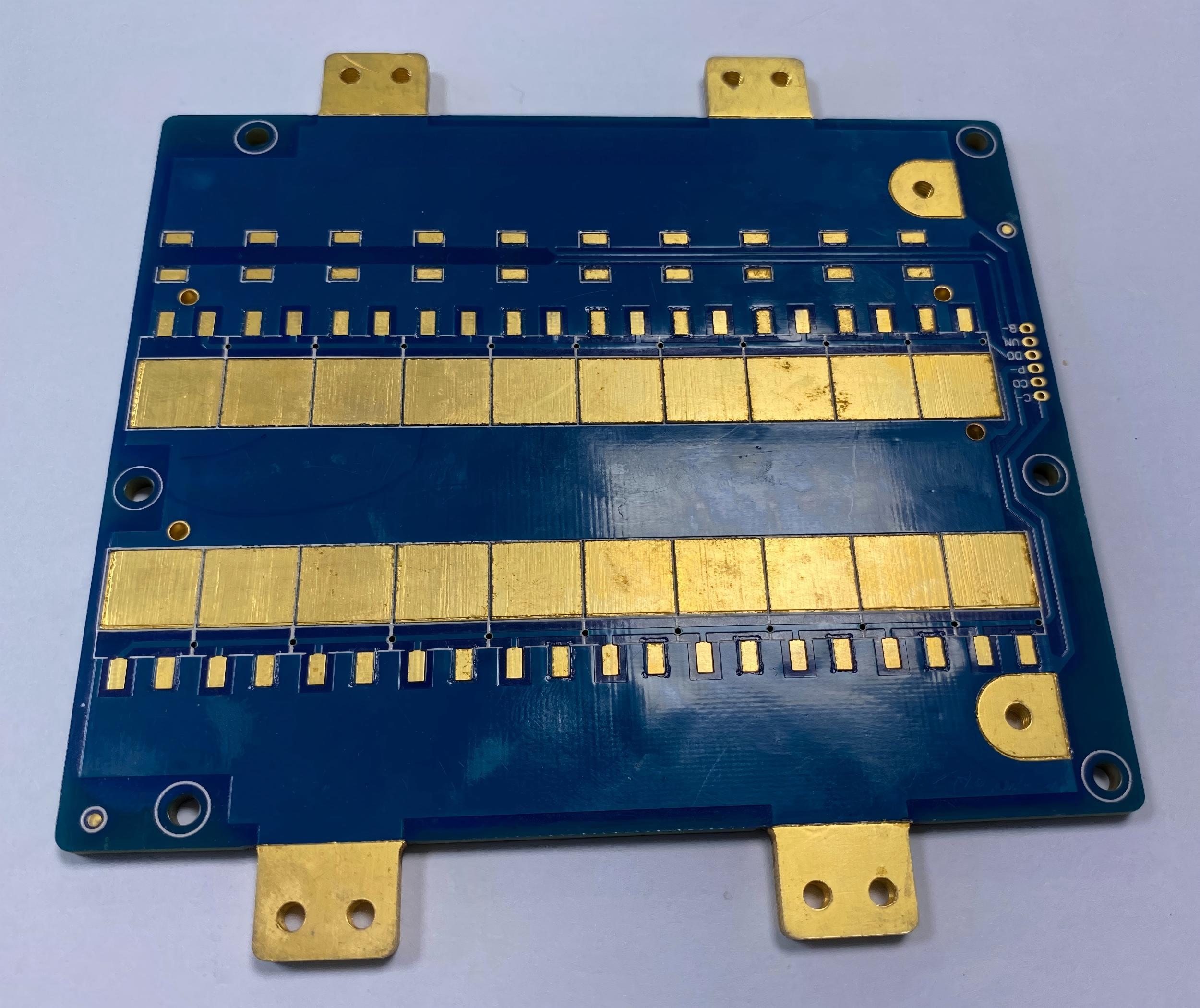
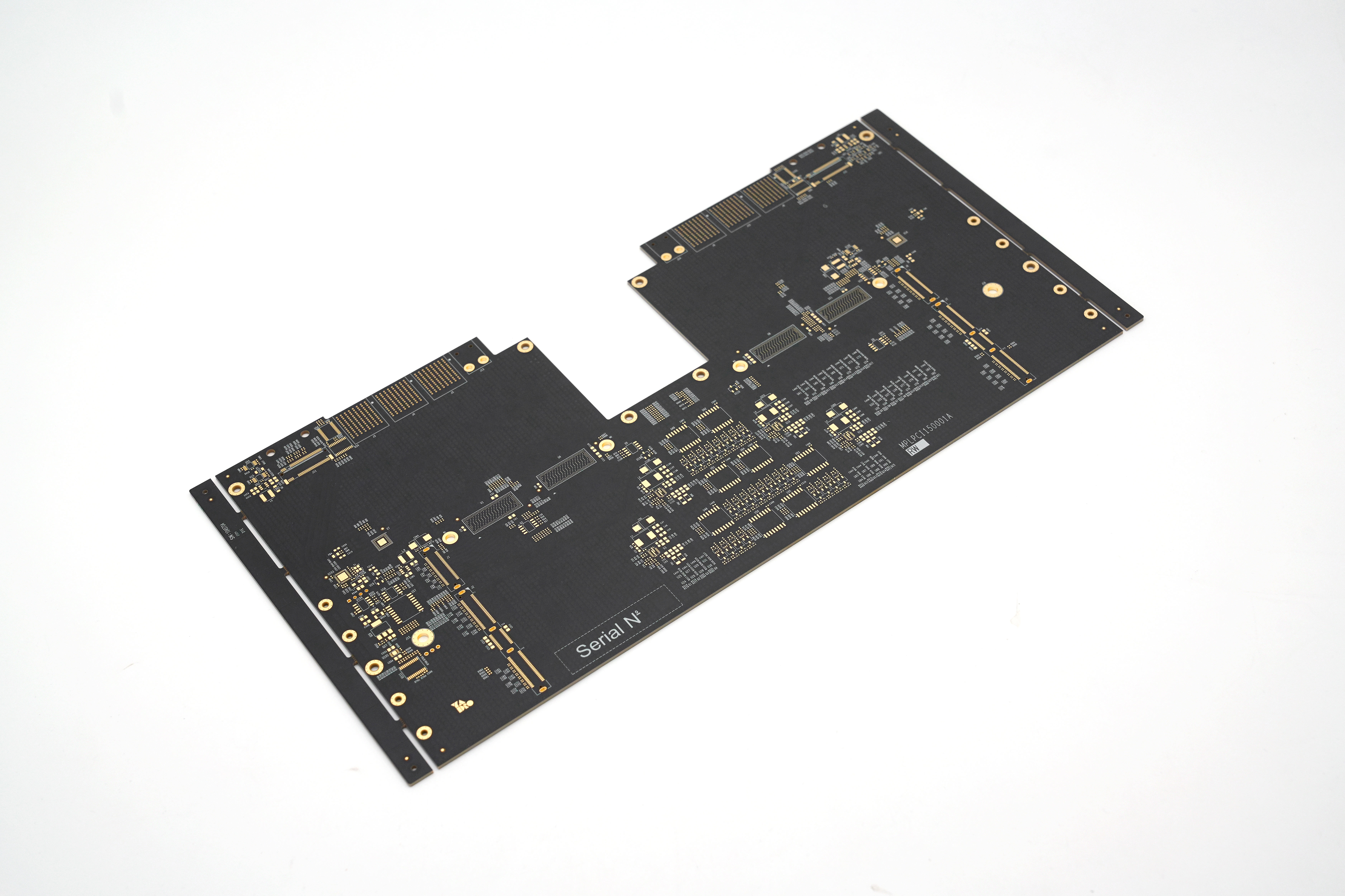
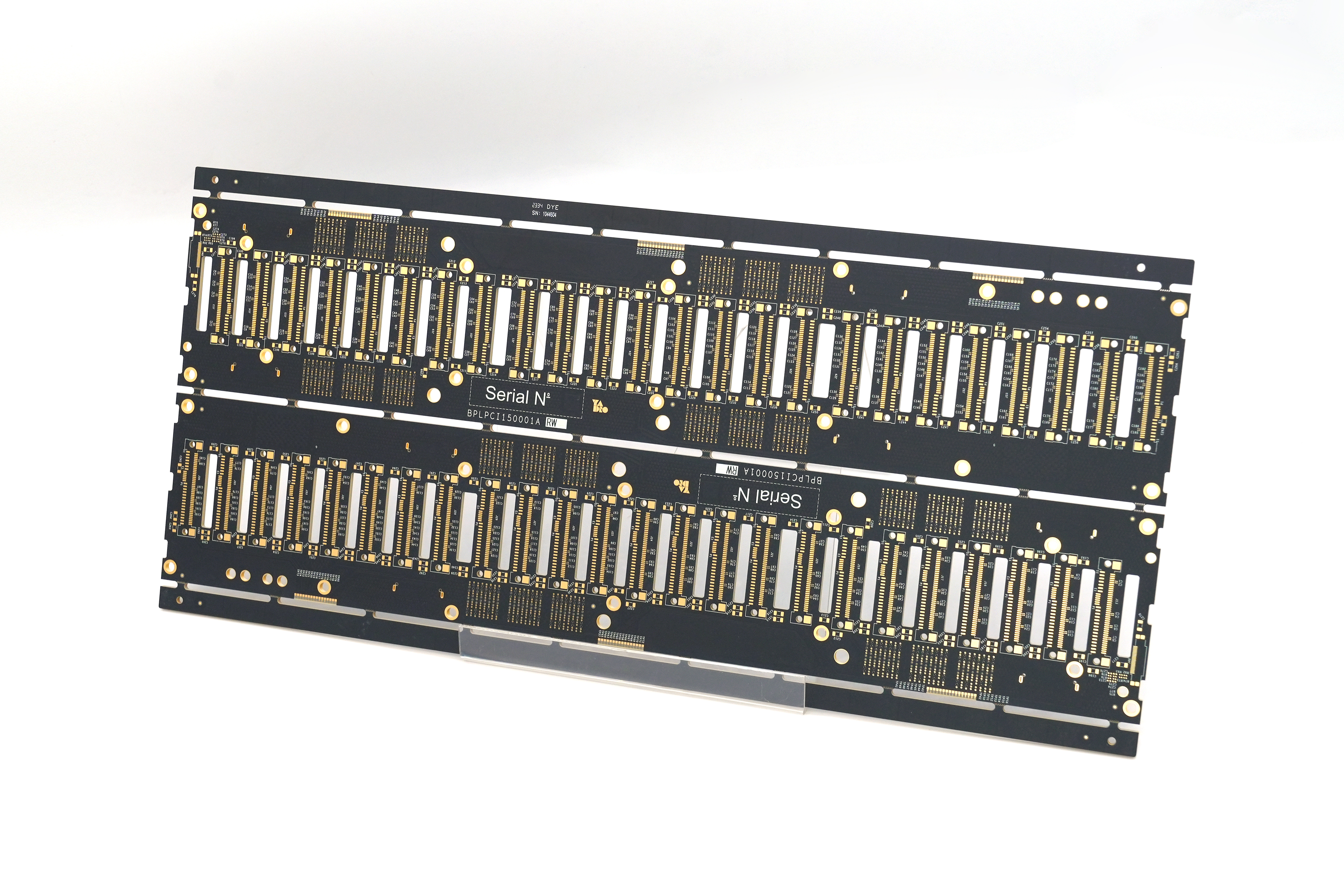
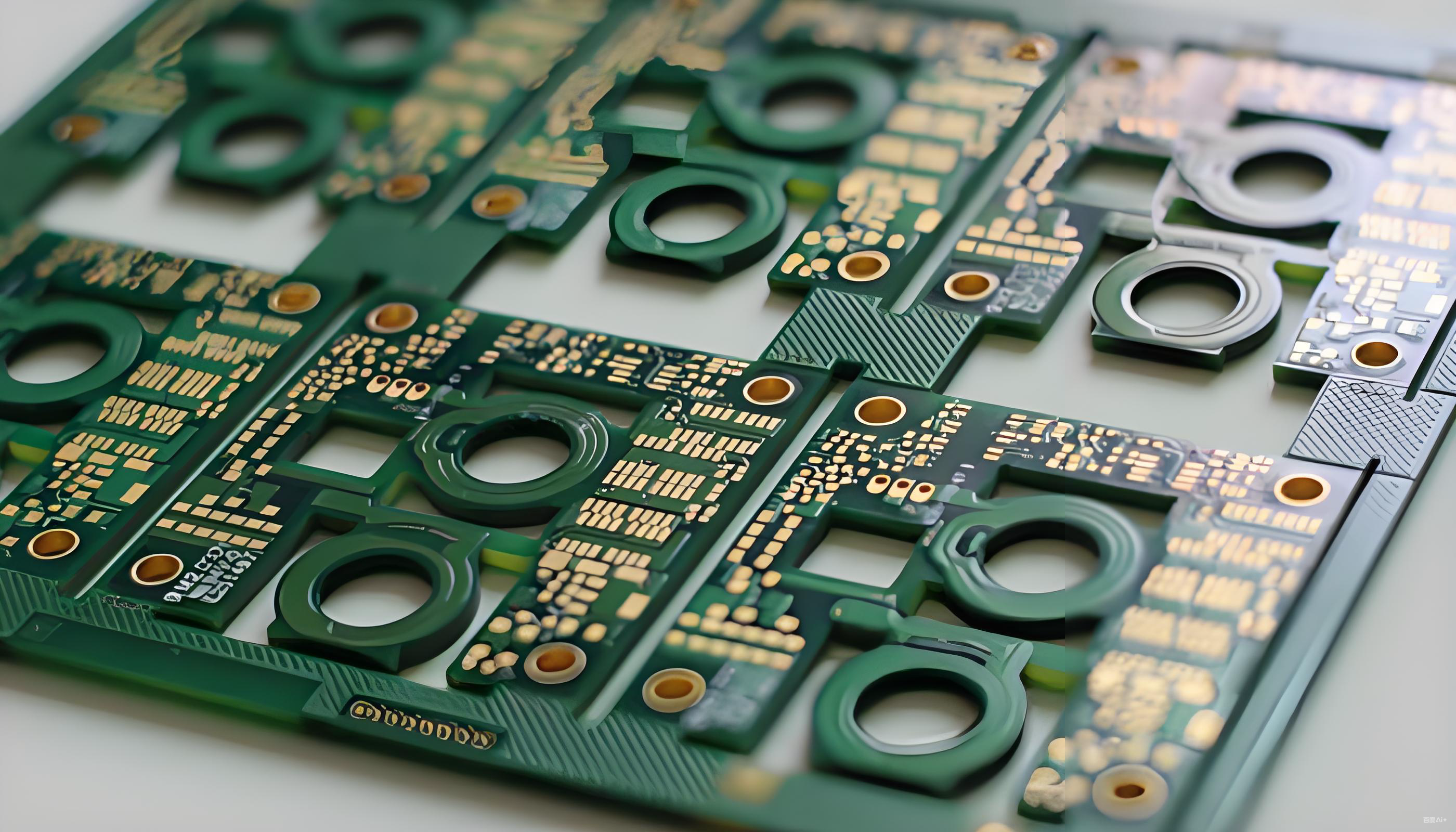
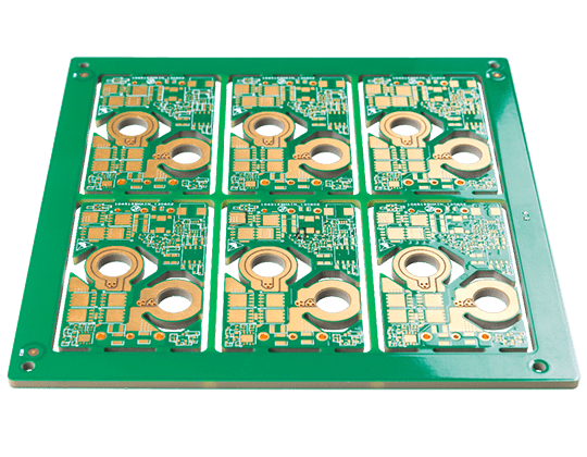
4. PCB Design & Manufacturing
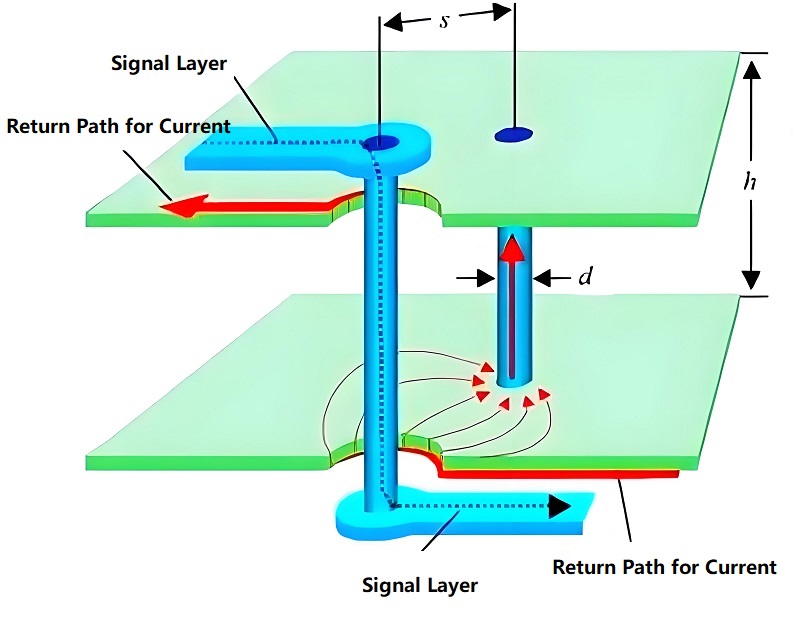
- Layout & Routing: Follow signal integrity: differential pairs for high-speed signals (ADC clocks, buses); separate analog/digital signals. Use star/mesh grounding to minimize noise; shield critical traces.
- Component Selection: Prioritize SMD packages (QFN, SOP) for size, consider solderability/thermal needs (heat sinks for power devices). Verify supply chain stability.
- DFM: Adhere to design rules (trace width/spacing, via size, impedance control) to avoid defects (opens/shorts). Add test points, labels, and mounting holes.
5. Testing & Debugging
- Hardware Testing: Validate power voltage, signal output, and ADC reference with oscilloscopes/multimeters. Test isolation, input impedance, and CMRR.
- Software Verification: Unit-test drivers (ADC read, data transfer); integrate-test workflows (multi-channel sync, upload). Use logic analyzers to verify protocols (SPI timing).
- System Tuning: Connect real sensors/signal sources to validate functions (temperature accuracy, vibration FFT). Adjust circuits (filter cutoff), algorithms (filter coefficients), or layout (ground plane splits) for optimization.
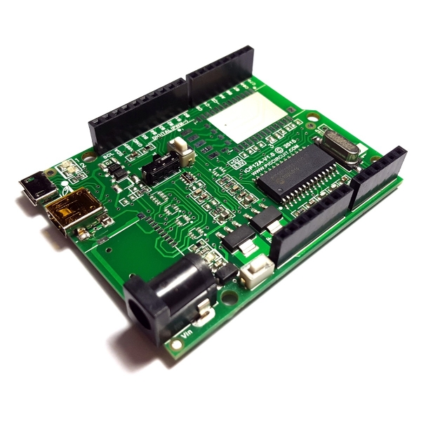
How to Connect Arduino to Data Acquisition Board?
1. Verify Compatibility and Interface Requirements
- Confirm communication protocols (UART, I2C, SPI, analog signals) supported by the data acquisition board.
- Match Arduino interface pins (e.g., SDA/SCL for I2C).
- Check voltage compatibility (use level shifter for 5V-3.3V mismatches).
- Prepare tools: DuPont wires, multimeter, breadboard.
2. Safe Physical Connection
- Power off devices before connecting.
- Align GND-GND, VCC-VCC connections.
- Pair signal wires correctly (TX-RX for UART, SDA-SDA/SCL-SCL for I2C).
- Use color-coded wires and anti-slip connectors.
- Secure with heat-shrink tubing to prevent loose contacts.
3. Power Supply Management
- Use external power adapter for high-power boards (>200mA).
- Calculate total current draw when sharing power (≤500mA Arduino limit).
- Add decoupling capacitors near power pins to reduce noise.
4. Software Setup and Validation
- Install official libraries in Arduino IDE.
- Test via serial monitor with sensors (e.g., temperature readings).
- Adjust baud rates (9600bps) for stable data transmission.
- Check for corrupt characters or data loss.
5. Troubleshooting Tips
- Inspect connections for loose wires or crossed TX/RX lines.
- Shorten wire lengths (<1m) or use shielded cables.
- Consult manufacturer documentation for device-specific issues.
- Regularly check wire integrity in industrial environments.
- Provide connection diagrams when seeking community support.
Why Choose EBest Circuit (Best Technology) as Data Acquisition Board Manufacturer?
Reasons why choose us as data acquisition board manufacturer:
- High-Precision SMT Automation Line: Equipped with imported high-precision pick-and-place machines (e.g., ASMPPT-5800) achieving ±0.08mm placement accuracy. Combined with X-ray/AOI dual inspection, it ensures defect-free soldering for micro-components (e.g., 0201 size), reducing client rework costs by over 30%.
- 24 Hours Rapid Prototyping Service: Dedicated NPI lines enable 48-hour engineering prototype assembly and functional verification. DFM software pre-screens design risks, shortening client product launch cycles by 2-4 weeks.
- High-Reliability Multi-Layer Board Assembly: Specialized vacuum lamination for 6-24 layer HDI boards with laser via detection ensures layer alignment ≤5μm, enhancing signal integrity. This raises client product pass rates in harsh environment tests (-40℃~125℃ thermal cycling) to 99.8%.
- Flexible Volume Production Capability: MES-monitored 18 production lines support seamless transition between 100-100,000 unit orders. Smart material management ensures zero BOM errors, improving client inventory turnover by 40% and eliminating dead stock losses.
- High-Density Hybrid Assembly Technology: Mastery of QFN/BGA/CSP hybrid assembly with selective wave soldering under nitrogen. Void rates in through-hole soldering are controlled below 2%, meeting AEC-Q100 automotive-grade reliability. Client product defect rates drop below 0.3%.
- Automated Functional Testing System: Self-developed ATE platform integrates multi-channel signal sources and precision measurement units for 100% full-function testing. Automatic firmware validation ensures 99.97% outbound quality, minimizing field failures.
- Lead-Free Environmental Compliance: Certified under ISO 14001 and RoHS 2.0, using lead-free solder and water-soluble flux. Waste gas/water treatment systems guarantee compliance with EU/NA environmental regulations, ensuring 100% export legality for client products.
- Expert Engineering Support Team: 20+ senior process engineers (avg. 10+ years’ experience) provide end-to-end support from DFM optimization to cost analysis and failure mode diagnostics. Client R&D efficiency improves by 50% with 3x faster problem resolution.
Welcome to contact us if you have any request for PCBA service: sales@bestpcbs.com.