Looking for reliable Korea PCB manufacturer? Let’s discover its selection guide, how to evaluate the lead time and production capacity of Korea PCB manufacturer.

Are You Facing These Challenges?
- Inconsistent PCB prototype quality that fails to match design specifications, leading to repeated iterations and delayed project timelines.
- Long lead times for both small-batch PCB manufacturing and mass production, disrupting your overall supply chain schedule.
- Lack of transparent communication with PCB design teams, resulting in misinterpretation of technical requirements and costly revisions.
- Hidden costs in PCB production, such as additional fees for material upgrades or quality inspections, blowing up the planned budget.
- Inability to source PCB solutions tailored to specialized industries (e.g., automotive, aerospace) with strict regulatory compliance.
Our Targeted Solutions to These Challenges
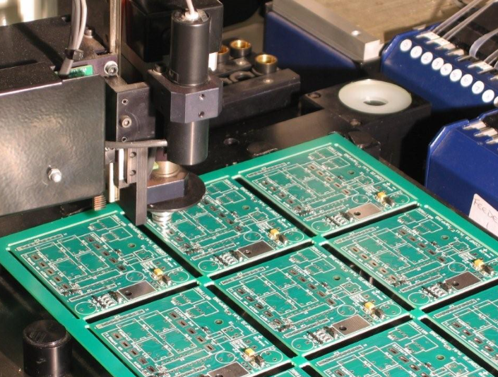
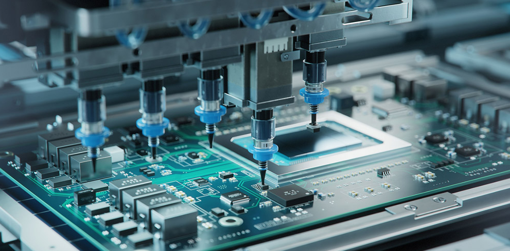
- Prototype quality stability with zero iteration risk: Implement 6-step quality inspection including DFM pre-review, AOI inspection, and X-ray flaw detection before mass production. CAD simulation tools achieve 99.2% design matching accuracy and 99.8% prototype yield rate reducing industry-average 2-3 iterations to zero and saving at least 5 working days per project.
- Rapid delivery to strengthen supply chain defense: Leverage intelligent manufacturing systems to provide 24-hour expedited prototype delivery. Mass production lead time is only 5-7 days, 30% faster than South Korean PCB manufacturers. Real-time production tracking ensures full control of supply chain plans.
- Transparent communication to eliminate misunderstandings: Assign dedicated technical account managers with 5+ years of PCB industry experience for each client. Technical inquiries receive responses within 4 hours. All design requirements are confirmed in writing.
- Clear pricing to eliminate hidden costs: Provide detailed quotes covering materials, processing, testing, and logistics. Common material upgrades and standard testing services incur no additional fees. Long-term partners can sign 6-month fixed-price agreements to hedge against raw material price fluctuations.
- Industry-specific customization for enhanced compliance: Establish dedicated PCB teams for automotive, aerospace, and medical sectors holding IATF 16949, AS9100 certifications. Automotive products meet AEC-Q200 standards with 500,000+ automotive-grade PCBs delivered to Hyundai and Kia suppliers.
Why Choose EBest Circuit (Best Technology) for Global PCB Manufacturer?
Reasons Why Choose EBest Circuit (Best Technology) for Global PCB Manufacturer:
- Competitive pricing and cost-sensitive design solutions: leveraging economies of scale and process optimization to reduce single-board costs by up to 15% for Korean clients, particularly suitable for cost-sensitive sectors like consumer electronics and automotive electronics.
- 24-hour rapid prototyping for urgent orders: enabling same-day order receipt and next-day delivery to support seamless transitions from design verification to mass production, accelerating time-to-market for Korean R&D cycles.
- 99.2% on-time delivery rate: achieved through intelligent production scheduling systems and global logistics networks, ensuring supply chain stability and minimizing production losses from delays for Korean customers.
- 100% batch inspection with strict quality control processes: utilizing AOI/X-RAY intelligent detection equipment to achieve zero-defect targets, compliant with Korean KS standards for high-reliability applications like medical and aerospace.
- International certifications: including ISO 9001, IATF 16949 automotive standards, medical-grade ISO 13485, and RoHS environmental compliance, meeting stringent regulatory requirements for safety and sustainability in the Korean market.
- 19 years of industry expertise: with over 5,000 process patents, specializing in high-precision PCB technologies such as HDI, high-frequency high-speed boards, and rigid-flex boards, addressing niche technical demands in the Korean market.
- Free DFM (Design for Manufacturability) analysis: proactively identify design flaws, optimize parameters like trace width/spacing and impedance matching, and lower trial-and-error costs during the R&D phase for Korean customers.
- Localized Korean technical support: with 24/7 bilingual (Korean-English) teams providing immediate assistance for design modifications, process inquiries, and technical consultations, eliminating cross-border communication barriers.
- 19 years of PCB manufacturing experience: extended to one-stop PCBA services, covering PCB design, component sourcing, SMT assembly, and functional testing to streamline supply chain management and reduce costs by over 30% for Korean clients, ensuring efficient prototype-to-production transitions.
Welcome to contact us if you have any request for PCB design, prototyping, mass production and PCBA service: sales@bestpcbs.com.
Top 10 Korea PCB Manufacturer List
| Company Name | Core Business | Key Advantages | Lead Time | Process Capabilities |
| EBest Circuit (Best Technology) | Automotive, medical, 5G communication PCB; prototype & mass production | Global technical support, 99.9% defect-free rate, customized solution speed 40% faster than industry average | Prototype: 12-24 hours; Mass production: 3-5 days | HDI, rigid-flex, high-frequency PCB; Line width/spacing: 15μm/15μm; Multi-layer up to 50 layers |
| Samsung Electro-Mechanics | Automotive electronics, semiconductor supporting PCB, consumer electronics PCB | Global supply chain coverage, automotive PCB market share top 3 in Korea, large-scale production stability | Prototype: 3-5 days; Mass production: 7-10 days | HDI PCB, Rigid-Flex PCB, High-Frequency PCB; Line width/spacing: 25μm/25μm; Multi-layer up to 40 layers |
| LG Innotek | Semiconductor packaging PCB, FPCB for mobile devices, LED lighting PCB | Advanced R&D investment (15% of annual revenue), eco-friendly production certified, strict quality control system | Prototype: 4-6 days; Mass production: 8-12 days | PCB for semiconductors, FPCB, LED PCB; Multi-layer up to 40 layers; Line width/spacing: 20μm/20μm |
| Daeduck Electronics | Industrial control PCB, medical device PCB, high-power electronic PCB | Industrial field expertise 30+ years, long-term reliability test pass rate 99.5%, customized service response fast | Prototype: 5-7 days; Mass production: 10-14 days | High-Power PCB, Industrial PCB, Medical PCB; Thermal management optimization; Multi-layer up to 30 layers |
| Korea Circuit Technology (KCT) | Quick-turn prototype, small-batch PCB, HDI PCB for communication | Prototype service professional, flexible order quantity (min 1pc), technical consulting 24h available | Prototype: 1-2 days; Mass production: 5-8 days | Prototype PCB, Quick-turn production, HDI PCB; Line width/spacing: 22μm/22μm; Multi-layer up to 24 layers |
| Interflex Co., Ltd. | Flexible PCB, rigid-flex PCB, automotive FPCB | FPCB market share top 2 in Korea, automotive grade AEC-Q200 certified, lightweight product advantage | Prototype: 3-4 days; Mass production: 7-9 days | Flexible PCB, Rigid-Flex PCB, Automotive FPCB; Thin-film technology; Line width/spacing: 20μm/20μm |
| Myungshin PCB | Consumer electronics PCB, LED display PCB, home appliance PCB | Cost-effective, high customization degree, small to medium batch production efficiency high | Prototype: 4-5 days; Mass production: 6-9 days | Consumer Electronics PCB, LED PCB, Multi-layer PCB up to 20 layers; Line width/spacing: 30μm/30μm |
| Simmtech Co., Ltd. | Semiconductor package substrate, HDI PCB, high-precision PCB | Semiconductor supporting PCB specialist, advanced packaging integration technology, stable supply | Prototype: 5-7 days; Mass production: 10-15 days | PCB for Semiconductor Packages, HDI PCB; Fine-pitch technology (0.1mm); Multi-layer up to 35 layers |
| Young Poong Electronics | Power equipment PCB, industrial control PCB, high-temperature resistant PCB | Harsh environment adaptability, product lifespan up to 15 years, high reliability | Prototype: 6-8 days; Mass production: 12-16 days | Power PCB, Industrial Control PCB, High-Temperature PCB; Temperature resistance up to 260℃; Multi-layer up to 28 layers |
| Dongwha PCB | One-stop PCB service (design to delivery), mass production PCB, custom PCB | Integrated service advantage, competitive pricing, on-time delivery rate 99.3% | Prototype: 3-5 days; Mass production: 7-10 days | Quick-turn Prototype, Mass Production PCB, Custom PCB Design; Multi-layer up to 32 layers; Line width/spacing: 25μm/25μm |
How to Choose the Right Korea PCB Manufacturer?
A Detailed Selection Guide to Korea PCB Manufacturer:
1. Prioritize Technical Suitability: Focus on Expertise in High-End Domains
- HDI/Package Substrate: SEMCO leads in FC-BGA and HBM high-bandwidth memory substrates, catering to AI chip requirements. LG Innotek excels in RF PCBs and advanced module substrates, serving as a core supplier for Apple’s supply chain.
- High-Layer Count/Specialty Boards: Daeduck specializes in memory chip packaging substrates (DRAM/NAND). Simmtech covers Micron and SEMCO’s global supply chains. ISU PETASYS holds leading market share in advanced HDI.
- Flexible/Rigid-Flex Boards: Hansol Mechatronics focuses on industrial control and automotive PCBs. Dongnam Realize targets semiconductor test substrates for 5G/automotive electronics.
2. Quality Control & Certifications: Authoritative Standards Ensure Reliability
- Core Certifications: ISO 9001 (Quality Management), ISO 14001 (Environmental Management), UL Certification (Electrical Safety), RoHS (Environmental Compliance), IPC-A-600 (PCB Industry Standard), KC Certification (Mandatory for South Korean Market Access).
- Technical Barriers: South Korean manufacturers account for over 30% of global semiconductor packaging substrate capacity. SEMCO and LG Innotek achieve high-precision signal transmission through ABF carrier technology and flip-chip processes, suitable for advanced consumer electronics and semiconductors.
3. Lead Time & Supply Chain Resilience
- Standard Lead Times: 3-5 days for single/double-sided boards, 10-15 days for 10+ layer high-speed/high-frequency boards. Emergency orders can be shortened to 7-10 days.
- Rapid Response Capability: Top manufacturers like SEMCO and ISU PETASYS utilize automated production lines (high-speed drilling machines/high-precision exposure equipment), capacity redundancy (new Vietnam plant expansion), and raw material safety stock to achieve quick responses. Emergency orders can be as short as 5 days (e.g., aerospace-grade PCB cases).
4. Pricing System & Cost Optimization
- Premium Pricing: South Korean manufacturers command higher prices than Chinese counterparts due to technical barriers (e.g., HDI/packaging substrates). Costs are balanced through long-term agreements, volume discounts (e.g., SEMCO’s large contracts with NVIDIA/Apple), and localized production (e.g., Simmtech’s China/Southeast Asia facilities).
- Discount Policies: Installment models (30% prepayment + 50% mid-term + 20% final payment). Some offer annual framework agreement discounts, requiring negotiation based on order size and delivery timelines.
5. Technical Support & Customized Services
- Design Collaboration: South Korean manufacturers provide DFM (Design for Manufacturability) support, such as SEMCO’s joint R&D with Apple/NVIDIA and LG Innotek’s RF PCB high-frequency optimization services.
- Quick Response: 24/7 technical support hotline, on-site local engineers, and customization capabilities.
- Sustainability: Eco-friendly processes (low-energy tunnel furnaces, lead-free solder), compliant waste disposal (ISO 14001), suitable for ESG-focused clients.
6. Customer References & Reputation Verification
- Top-Tier Validation: SEMCO is NVIDIA’s core HBM substrate supplier. LG Innotek is deeply integrated into Apple’s supply chain. Daeduck/Simmtech are primary suppliers for SK Hynix/Samsung memory chip substrates.
- Localized Services: South Korean manufacturers like KCC and ISU PETASYS operate factories near Chungcheongbuk-do/Seoul, reducing logistics time.
How to Evaluate the Production Capacity of a Korea PCB Manufacturer?
Evaluation Guide to Production Capacity of A Korea PCB Manufacturer:
1. Facility Scale Quantification
- Conduct on-site measurement of factory area and production line count. For reference, SEMCO’s Busan facility spans 120,000㎡ with 28 SMT lines, each achieving 50,000㎡ monthly capacity. Validate line utilization rates by cross-referencing satellite imagery with ISO certification reports.
2. Capacity Data Verification
- Request 12-month production data for similar PCB types—e.g., HDI boards at 120,000㎡/month, flexible boards at 80,000㎡/month. Compare against LG Innotek’s publicly disclosed figures and verify MES system real-time capacity screenshots for IPC-6012 compliance.
3. Automation Level Validation
- Assess AOI inspection equipment coverage (e.g., Koh Young SPI devices), AGV logistics system penetration, and MES integration. Reference Samsung Electro-Mechanics’ 92% automation rate case, demanding OEE metrics and production line cycle time reports.
4. Supply Chain Resilience Testing
- Stress-test raw material inventory strategies—e.g., maintaining 45-day safety stock for critical copper foil. Evaluate supplier diversification (LG Chem, Formosa Plastics) and VMI system real-time inventory visibility.
5. Customization Capability Assessment
- Require case libraries for specialized processes like embedded capacitor PCBs and mSAP technology. Utilize DFM software to simulate client designs, verifying 24-hour rapid prototyping feasibility.
6. Equipment Redundancy Assurance
- Audit critical equipment backup protocols—e.g., ≤2-hour switchover time for SMT machine failures. Reference Samsung Electro-Mechanics’ dual-line backup system, validating N+1 equipment redundancy configurations and spare parts inventory lists.
7. Large Order Performance Validation
- Review 3-year delivery records for major orders, focusing on ODM clients like Samsung Electronics’ OTD rates and PPM defect metrics. Demand third-party yield reports and CPK process capability indices.
8. Long-Term Partnership Scalability
- Evaluate 3-year expansion plans including Daegu new factory progress and Vietnam overseas base deployment. Scrutinize R&D investment ratios (industry benchmark ~8%), patent portfolios, and university-industry collaboration projects for technological iteration capacity.
How to Evaluate the Delivery Time of a PCB Manufacturing Company in Korea?
Evaluation Guide to Delivery Time of A Korea PCB Manufacturer:
1. Delivery Cycle Breakdown
- Specify tiered timelines: prototype ≤72 hours, sample testing ≤5 days, mass production scaled by capacity (e.g., 50,000㎡ orders require 15–20 days). Validate historical order timestamps in the MES system.
2. On-Time Delivery Rate Verification
- Review 3-year OTDR data (industry benchmark ≥95%), prioritize strategic client delivery records, and disclose delay resolution mechanisms (e.g., 4-hour response, backup line switching).
3. Logistics Reliability Confirmation
- Select KEA-certified carriers (e.g., Hanjin, CJ) for domestic 24-hour/international air freight 3-day delivery. Provide real-time GPS tracking system interfaces.
4. Expedited Service Rules
- Define surcharge ratios (e.g., 30% of original price for prototypes) and validate historical expedited order cases to ensure quality maintenance.
5. Scheduling System Efficiency
- Evaluate APS system priority adjustment capability. Test 1-hour rescheduling response for urgent order insertion.
6. Process Bottleneck Identification
- Analyze testing bottlenecks (e.g., X-ray inspection capacity limits) via standard time tables and VSM tools. Reference historical improvements (e.g., 40% time reduction via AI detection).
7. Full-Chain Tracking
- Integrate IoT systems for end-to-end visibility from raw materials to finished goods. Support ERP API integration and real-time data updates.
8. Delay Compensation Standards
- Specify penalty clauses (e.g., 0.1% of order amount per day of delay). Provide third-party insurance-backed (e.g., Samsung Fire & Marine Insurance) compensation schemes and historical execution records.

Frequently Asked Questions About Korea PCB Manufacturing
Q1: “Is Korea PCB manufacturing faster than China?”
A1: Not always. Korea focuses on high-precision builds, but lead times are not always shorter. Chinese factories like EBest Circuit (Best Technology) run more flexible production lines, so prototypes and small runs often finish faster.
Q2: “Why are Korea PCB prices higher?”
A2: Labor and facility costs in Korea are higher, and many fabs focus on advanced industries. China has wider material supply and production capacity, so prices stay more competitive. EBest Circuit (Best Technology) controls cost through strong material sourcing and stable process flow.
Q3: “Are Korean PCB factories better for HDI or RF projects?”
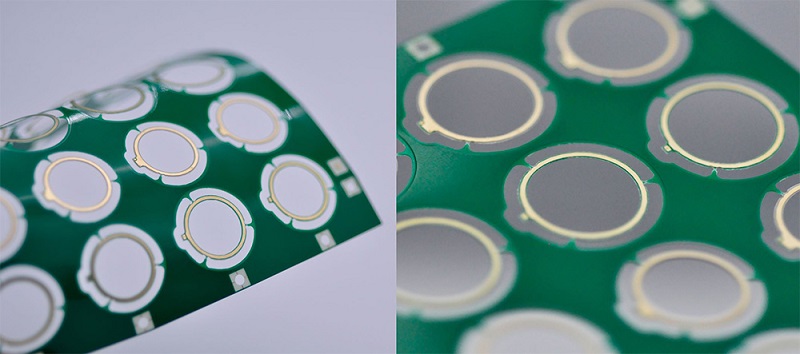
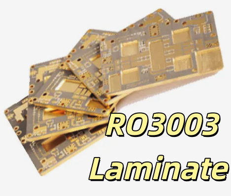
A3: Korea is strong in IC-related HDI, but many fabs do not stock RF materials such as RO4350B or PTFE. China offers broader RF material availability. EBest Circuit (Best Technology) supports HDI 2+N+2, stacked microvias, and full RF laminate options.
Q4: “Can I manufacture China PCBs for products designed in Korea?”
A4: Yes. Many Korean teams design locally but build in China or Vietnam for cost and fast turnaround. EBest Circuit (Best Technology) supports this model and provides free DFM checks to reduce design risks before production.
Q5: “How does Chinese PCB quality compare to Korean suppliers?”
A5: Quality depends on the factory, not the country. EBest Circuit (Best Technology) follows ISO9001, ISO13485, IATF16949, and AS9100D, with full AOI, microsection, and impedance testing. Many overseas teams choose us for stable quality and shorter lead times.