PCB RF shield may refer to both the shielding structure integrated into the PCB layout and the metal RF shielding can assembled onto the board. This guide delves into the strategies for optimizing your PCB layout to work seamlessly with board level shielding, enhancing the performance of your RF shielding PCB.
Even with a high-quality PCB mount RF shield, a poor underlying layout can render it ineffective, leading to failed emissions tests, degraded wireless performance, and costly redesigns. Common Pain Points When Integrating PCB RF Shields:
- Compromised Performance: Shielding can create unintended parasitic capacitance or cavity resonances that degrade the very RF signals you’re trying to protect.
- Thermal Traps: A solid RF shield box PCB can trap heat from power components, leading to overheating and reduced reliability.
- Layout Inflexibility: The footprint of a PCB RF shield frame and lid can force suboptimal component placement, increasing trace lengths and potential crosstalk.
- Assembly and Rework Headaches: Poorly planned keep-out areas can make PCB shield soldering difficult and rework nearly impossible without damaging the board.
- Ineffective Grounding: Without a low-impedance ground connection around the entire shield perimeter, PCB EMI shield effectiveness is drastically reduced, allowing noise leakage.
The key to overcoming these challenges lies in proactive, shield-aware layout planning. As a professional RF PCB manufacturer, BEST Technology addresses these issues by integrating shielding considerations from the earliest design stages.
- Co-Design for RF and Shielding: We model shield interactions during PCB RF design to pre-empt parasitic effects and optimize component placement.
- Strategic Thermal Management: Our layouts incorporate thermal vias, exposed pads, and planned airflow paths under custom PCB RF shield cans to prevent overheating.
- Layout Optimization for Shield Footprint: We prioritize critical RF trace routing and component placement first, designing the PCB multi-compartment RF shield footprint around the optimal layout, not the other way around.
- DFM for Shield Assembly: We enforce clear keep-out zones and provide solder paste recommendations to ensure reliable, reworkable assembly of RF shields PCB.
- Robust Grounding Strategy: We implement a “stitched” ground via perimeter directly under the shield solder lands to create an impeccable RF ground connection for the PCB RF shielding.
At BEST Technology, we specialize in the design and manufacturing of advanced RF and microwave PCBs, where effective PCB RF shields are not an afterthought but a core component of the layout architecture. Our expertise ensures your design achieves optimal performance and passes compliance testing seamlessly. Pls feel free to contact our engineering team at sales@bestpcbs.com to discuss your project.
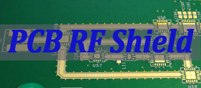
What Is a PCB RF Shield?
In essence, a PCB RF Shield refers to a form of board level shielding implemented at the printed circuit board level to suppress unwanted electromagnetic radiation and coupling. Its primary function is to form a localized Faraday cage around noise-generating or noise-sensitive circuits, thereby minimizing radiated interference and improving RF system stability.
In modern electronics, PCB RF shielding is commonly realized using several approaches:
- Shield Cans (PCB RF Shield Can)
One-piece or two-piece (frame + lid) metal enclosures soldered directly onto the PCB. They provide flexible coverage and are widely used for prototyping, RF modules, and large-area shielding. - Multi-Compartment Shields (PCB Multi-Compartment RF Shield)
Shields with multiple isolated cavities within a single frame, enabling different functional blocks—such as Bluetooth, Wi-Fi, and power management circuits—to be electromagnetically isolated on the same board. - Formed Sheet Metal Shields
Custom-formed metal shields tailored to complex PCB geometries, commonly adopted in high-volume consumer electronics where mechanical integration and cost efficiency are critical. - Conformal Shielding
Conductive coatings applied by spraying or plating directly over components. This approach is suitable for ultra-compact designs but offers limited shielding effectiveness at higher frequencies due to reduced thickness, grounding continuity, and cavity formation.
Selecting the appropriate PCB RF shielding approach depends on operating frequency, isolation requirements, available board space, thermal constraints, and the intended assembly process.
How Board Level Shielding Is Implemented in Multilayer RF PCB Design?
Implementation is a strategic process integrated into the stack-up and layout. It starts with planning.
- Shield Wall Vias: A continuous row of grounded vias around the shield perimeter connects all relevant ground planes, forming a low-impedance “wall” that prevents fields from leaking underneath.
- Dedicated Shield Ground Plane: A continuous, unbroken ground layer (often L2) directly underneath the shield area provides the primary reference and return path.
- Internal Cavity Control: For multi-compartment RF shields, internal ground walls defined by vias must extend through the board to isolate cavities at the internal ground plane level as well.
- Antenna Keepouts: Clear zones must be defined in the layout where no ground or shield can extend, ensuring antenna performance is not detuned.
Effective implementation turns the PCB with RF shield into a predictable, high-performance system rather than a mere add-on.
Understanding PCB EMI Shield for Noise Control in High-Frequency Circuits
At high frequencies, every trace is a potential antenna, and every loop is a receiver. A PCB EMI shield works by:
- Reflection: The conductive surface reflects incoming radiated energy.
- Absorption: Energy that penetrates the surface is attenuated as eddy currents, converting it to negligible heat.
- Grounding: The absorbed currents are safely shunted to ground via the low-impedance connection.
The shielding effectiveness (SE) is quantified as:
SE (dB) = R (dB) + A (dB) + M (dB)
Where R=Reflection Loss, A=Absorption Loss, and M=Multiple Reflection Loss. For effective RF shielding PCB, a good ground (maximizing R) and adequate material thickness (maximizing A) are critical.
Design Principles Behind Effective RF Shielding PCB in Wireless Applications
| Principle | Description | Layout Optimization Action |
|---|---|---|
| Continuous Grounding | Provides a low-impedance path for shield currents. | Create a via fence around shield footprint. |
| Minimizing Apertures | Any gap leaks RF energy; the largest dimension dictates the highest frequency leaked. | Place shield solder lands over solid ground. Keep slots/seams away from noise sources. |
| Cavity Resonance Control | The shielded cavity can resonate at certain frequencies, amplifying noise. | Strategically place absorbent materials or SMT components inside to disrupt resonant modes. |
| Signal & Power Integrity | Shield should not disrupt critical transmission lines or power distribution. | Route high-speed traces on layers adjacent to the shield ground plane. Use dedicated filter feedthroughs for power lines entering the shield. |
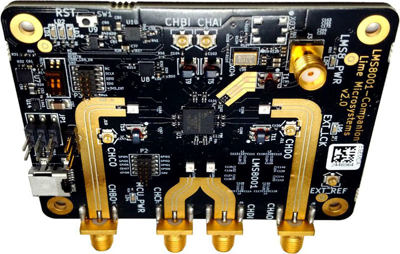
When to Use a PCB RF Shield Can and How It Integrates with PCB Layout?
Use a PCB RF shield can when you need to isolate a specific functional block (e.g., an RF transceiver, a switching regulator, a digital processor) post-layout, or when compartmentalization is needed. Integration is key:
- Placement: Position the can so its walls do not cut through critical impedance-controlled traces. Plan the footprint early.
- Grounding Pad Design: Provide a sufficient pad width (typically 0.5-1.0mm) on the PCB for the shield frame to solder onto, backed by the via fence.
- Internal Component Height: Ensure all components inside the RF shield PCB mount area are lower than the can’s inner height, with adequate clearance.
- Test Points & Rework: Provide external test points for signals inside the shield. Consider how the lid will be removed for rework without damaging surrounding components.
Assembly Considerations for PCB Mount RF Shield in Volume Production
A design that cannot be assembled reliably will fail in production.
- Solder Paste Stencil: The shield frame pads require a specific stencil aperture design (often a grid of small apertures) to prevent tombstoning or voiding during reflow.
- Pick-and-Place: Shield cans are heavy. Robust solder paste volume and potential use of adhesive are needed to prevent displacement.
- Automated Optical Inspection (AOI): Shield cans can obscure view of components underneath. Plan for pre-shield AOI or use shields with inspection holes.
- Rework Process: Design allows space for a soldering iron tip or hot-air nozzle to remove the shield without collateral damage.
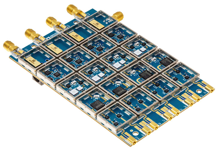
Advanced Isolation Using PCB Multi-Compartment RF Shield for Dense RF Modules
In modules combining, for example, 5G, GPS, and Wi-Fi, a PCB multi-compartment RF shield is essential.
- Cross-Talk Suppression: Internal walls provide >60dB of isolation between compartments, preventing oscillator pulling and noise coupling.
- Shared Ground Reference: The single frame ensures all compartments share the same ground potential, critical for mixed-signal performance.
- Layout Efficiency: Enables tighter integration of multiple RF systems on a single board than using multiple individual cans.
- Design Complexity: Requires precise alignment of internal PCB ground segmentation with the shield’s internal walls.
Why Select EBest Circuit (Best Technology) for Delivering Custom PCB RF Shielding from Design to Assembly?
Selecting a manufacturing partner for Radio Frequency (RF) shielding is a critical decision that directly impacts the performance, reliability, and time-to-market of your electronic products. It requires more than just basic PCB fabrication; it demands a deep understanding of high-frequency materials, precision engineering, and seamless integration between design, board fabrication, and assembly.
1. Unmatched Material Expertise and Fabrication Precision for RF Applications
RF circuits are exceptionally sensitive to signal loss and interference. EBest Circuit (Best Technology)’s capabilities, as detailed in their PCB Process Capability Sheet, demonstrate a foundation built for high-frequency success:
- Extensive Material Portfolio: They are proficient with a wide range of standard and specialized RF substrates, including:
- Standard Low-Loss: KB 6160, ShengYi S1141
- Very Low-Loss: Rogers 4350B, Rogers 4003, Taconic series, Arlon series.
- Halogen-Free Options: KB 6165, IT 158, ShengYi S1150G.
- This versatility ensures they can recommend and process the ideal material for your specific frequency and loss tangent requirements, rather than forcing a one-size-fits-all solution.
- Precision Controlled Impedance: Maintaining consistent impedance is non-negotiable for RF integrity. EBest Circuit (Best Technology) guarantees tight impedance control with a standard tolerance of ±5Ω (<50Ω) or ±10% (≥50Ω), and an exceptional limit of ±4Ω or ±6% for prototype orders. This level of precision minimizes signal reflection and ensures design performance is realized in the final product.
- Advanced Drilling and Microvia Technology: RF shielding often requires complex via structures for grounding and isolation. Their capabilities are state-of-the-art:
- Laser Drilling: Capable of producing microvias as small as 0.070mm (limit) with an aspect ratio of 1:1.
- Mechanical Drilling: Standard capabilities down to 0.10mm, handling high aspect ratios up to 12:1 (standard) and an extreme 25:1 (limit).
- This allows for dense, effective via fencing around critical components, a cornerstone of effective PCB-level RF shielding.
- Fine-Line Circuitry: To accommodate complex RF layouts, they can produce traces and spaces as fine as 2.5/2.5 mil (limit for 1/2 oz copper), with standard capabilities of 3/3 mil.
2. Seamless Design-for-Manufacturability (DFM) Integration
The greatest RF design will fail if it is not manufacturable. EBest Circuit (Best Technology)’s engineers engage early in the design process, leveraging their comprehensive capability data to advise on:
- Optimal Layer Stack-up: With experience building boards from 1 to 50 layers (standard) and up to 100 layers (limit, upon review), they can help optimize your stack-up for shielding effectiveness, incorporating dedicated ground planes and minimizing parasitic effects.
- Material Selection: They guide the trade-offs between cost, performance, and processability, ensuring your chosen RF material is compatible with the rest of the board’s construction.
- Shielding Canopy Design: They provide expert DFM feedback on solder pad layouts, aperture sizes, and placement to ensure a reliable mechanical and electrical seal for attached shielding cans.
3. True End-to-End Control: From Bare Board to Protected, Assembled PCB
This is EBest Circuit (Best Technology)’s most significant advantage. By managing the entire process under one roof, they eliminate the finger-pointing, logistical delays, and quality variances common with using multiple vendors.
- Integrated PCBA Services: Their assembly division supports:
- Advanced Components: Handling complex ICs, RF modules, and fine-pitch BGAs.
- Shielding Can Implementation: Precise soldering or adhesive attachment of custom fabricated shielding cans.
- Conformal Coating & Potting: For environmental protection of the assembled board, including the shielded areas.
- Box-Build Assembly: Final integration into enclosures, providing a complete turnkey product.
- Guaranteed Compatibility: The assembly team uses the same design data and works directly with the fabrication team. This ensures that the finished PCB is perfectly suited for the subsequent assembly and shielding processes, preventing issues like warpage during reflow or poor solder joint formation on shielding cans.
| Feature | EBest Circuit (Best Technology)’s Capability | Benefit for Your RF Shielding Project |
|---|---|---|
| Material Expertise | Rogers, Taconic, Arlon, etc. | Optimal signal integrity & minimal loss at high frequencies. |
| Impedance Control | ±5Ω / ±10% (Standard) | Predictable performance, reduced signal reflection. |
| Microvia Precision | 0.070mm laser drills | Dense via fencing for superior isolation. |
| Vertical Integration | Design → Fabrication → Assembly | Faster turnaround, single quality responsibility, superior DFM. |
EBest Circuit (Best Technology) stands out by offering a truly integrated, “One-Stop Solution” from design consultation to final box-build assembly, backed by quantifiable technical capabilities that ensure superior RF shielding performance. For your next custom PCB RF shielding project, pls feel free to connect with EBest Circuit (Best Technology) via sales@bestpcbs.com. We have the full technical capability to deliver high-quality RF shield PCBs from design to assembly as quickly as possible.
Finally, a PCB RF shield is an indispensable tool for containing electromagnetic interference and ensuring the reliable operation of modern high-frequency electronics. This article has outlined the key principles for optimizing your PCB layout to maximize the effectiveness of RF shields for PCB applications.
Success hinges on co-designing the shield and the layout from the start, focusing on robust grounding, thermal management, and manufacturability. BEST Technology possesses the specialized PCB RF design expertise and manufacturing precision to navigate these complexities. We ensure your PCB with RF shield is not just assembled, but engineered for peak performance. For your next project, pls feel free to reach out to our team at sales@bestpcbs.com.
FAQs
Is a PCB RF Shield Necessary for All RF and Microwave PCB Applications?
Not always. For simple, low-power, or low-frequency designs, careful layout and filtering may suffice. However, for most modern wireless, high-speed digital, or sensitive analog designs—especially those requiring regulatory certification (FCC, CE)—a PCB RF shield is a critical and cost-effective component for ensuring compliance and reliable performance.
What Materials Are Commonly Used for a PCB RF Shield and Why?
- Brass or Stainless Steel with Nickel Plating: Excellent shielding effectiveness, good solderability, and cost-effective for RF shield PCB mount cans.
- Copper Alloys (e.g., C7521 Nickel Silver): Superior high-frequency performance due to higher conductivity, often used in demanding RF PCB applications.
- Tin-Plated Steel: A lower-cost alternative, suitable for less demanding frequency ranges. The choice balances performance, cost, corrosion resistance, and solder joint reliability.
How Thick Should a PCB RF Shield Be for Effective EMI Suppression?
Thickness primarily affects absorption loss (A). For most board level shielding applications in consumer electronics, shield can thickness ranges from 0.1mm to 0.2mm.
This provides sufficient absorption above 1 GHz. The grounding quality (via fence) is often more critical than minimal extra thickness. For extreme high-power or low-frequency magnetic shielding, thicker materials or specialized alloys like MuMetal may be required.