Remote controlled circuit is an electronic system that wirelessly receives commands from a transmitter and converts them into electrical signals that control a device or operation without physical connection. This article explores remote control circuit definition, the design principles, working mechanisms, and best practices for building reliable remote controlled circuits, focusing on the critical components and PCB solutions that power high-performance RC car electronics.
Designing and manufacturing a robust remote control circuit for an RC car involves navigating a complex array of technical and production challenges. Are you struggling to tackle these common pain points?
- Unreliable Wireless Links: Signal dropouts, interference, and limited range degrade control stability and user experience.
- Motor Noise and Power Issues: Motor-induced noise and poor power regulation cause resets and control instability.
- Bulky or Inflexible Designs: Oversized or rigid layouts limit compact, customized RC car designs.
- Fragile Constructions for Demanding Use: Vibration, impact, and stress expose weak PCB structures in consumer RC cars.
- Scaling from Prototype to Volume Production: Moving from a simple remote control circuit to a mass-producible remote control car PCB circuit is complex.
The key to overcoming these obstacles lies in a holistic approach that integrates intelligent circuit design with professional manufacturing expertise. Here are five core solutions:
- Employ Robust RF Protocols & Shielding: Proven RF modules, solid grounding, and shielding ensure stable, interference-resistant control.
- Implement Dedicated Power & Motor Drive Stages: Isolated motor drivers and clean power routing protect control logic from noise.
- Adopt High-Density Interconnect (HDI) PCB Technology: Multilayer HDI boards reduce size while improving signal integrity and integration.
- Specify Durable FR-4 Materials & Coatings: High-Tg FR-4 and conformal coatings enhance durability in remote control car applications.
- Partner with an Experienced Volume PCB Producer: Automated assembly and testing enable smooth scaling from remote control circuit diagram to production.
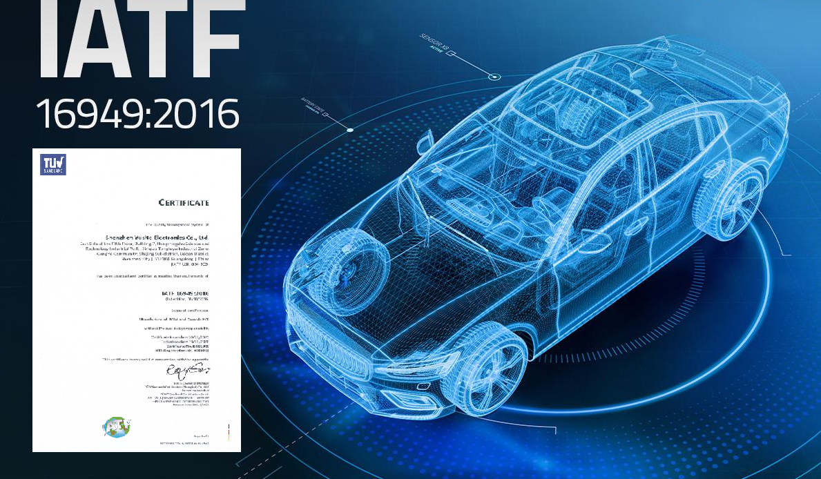
At BEST Technology, we are a specialized PCB and assembly factory with 19 years of deep expertise in supporting electronics innovators. We understand that a reliable remote control car circuit board is the foundation of a great product. Our strength lies in turning complex designs into high-performance, manufacturable realities. From offering design-for-manufacturability (DFM) feedback on your RF remote control circuit diagram to delivering robust, coated PCBs ready for assembly, we ensure quality at every step. Pls feel free to contact our team at sales@bestpcbs.com for new inquires.

What Is a Remote Controlled Circuit?
What is remote control circuit definition? A remote controlled circuit is a system comprising a transmitter and a receiver that enables wireless command over a device’s functions. In essence, it creates a wireless communication link to bridge the gap between user input and machine action. In the context of RC cars, this remote controlled circuit is responsible for interpreting throttle, steering, and auxiliary commands (like lights or winches) and executing them via motors and servos.
- Core Function: To provide reliable, low-latency, and secure wireless control.
- Key Segments: The system is always bipartite:
- Transmitter: The handheld controller held by the user. It encodes control stick positions into a modulated signal.
- Receiver: Housed within the RC car. It demodulates the received signal and outputs corresponding control signals to the Electronic Speed Controller (ESC) and servos.
- Control Types: Commands can be analog (proportional control for smooth steering/throttle) or digital (on/off for accessories).
- Modern Integration: Advanced systems may include telemetry, allowing the car to send data (like battery voltage) back to the transmitter.
Fundamentally, a remote control circuit replaces physical wires with a wireless protocol, granting the freedom of movement that defines the RC experience.

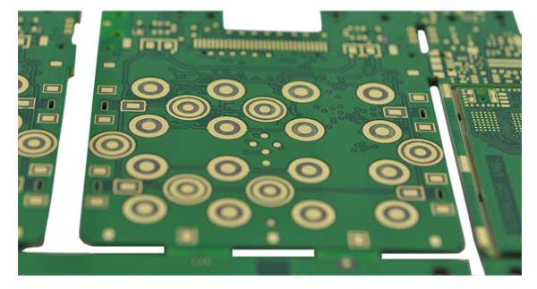
What Materials Are Best for a Remote Controlled Circuit Board?
The choice of PCB substrate material is critical for the performance, durability, and cost of your remote control car PCB circuit. It must withstand operational stress while ensuring signal integrity.
- FR-4 (Epoxy Glass): The industry standard and most cost-effective choice.
- Ideal for: Most hobbyist and consumer-grade RC cars.
- Advantages: Good mechanical strength, excellent electrical insulation, and easy manufacturability.
- Consideration: Standard FR-4 can be susceptible to moisture absorption; specify high-Tg (glass transition temperature) versions for better thermal performance in demanding environments.
- Polyimide (PI): A high-performance flexible material.
- Ideal for: Applications where the PCB must bend or fit into unconventional spaces.
- Advantages: Excellent flexibility, superior thermal resistance, and high durability.
- Consideration: Higher cost than FR-4, more challenging to process.
- Ceramic (Alumina, Aluminum Nitride): Used for specialized, high-reliability applications.
- Ideal for: Extreme environments (very high temperature, high frequency) or where superior thermal conductivity is needed to cool high-power components.
- Advantages: Exceptional thermal management, high-frequency performance, and hermetic sealing capability.
- Consideration: Significantly higher cost and fragile (brittle) compared to organic substrates.
In summary, for the vast majority of circuit board for remote control car projects, high-quality FR-4 is the optimal balance of performance, durability, and cost. Flexible Polyimide is chosen for unique form factors, while ceramic substrates are reserved for extreme-use cases.
How Does a Remote Control Car Circuit Work?
At its core, a remote control car circuit converts user input into wireless commands and translates them into precise motor and steering actions. This closed system relies on signal encoding, wireless transmission, decoding, and power-controlled execution, all coordinated in real time.
1. Command Initiation: Transmitter Input
User actions on the transmitter change potentiometer or switch states, which the onboard MCU converts into digital control data. These data packets include motion commands and a unique ID, then modulate an RF carrier (typically 2.4 GHz) or drive an IR LED in simpler systems.
2. Wireless Signal Transmission
The encoded signal travels through air as RF waves or infrared pulses. RF-based designs dominate due to longer range, obstacle tolerance, and interference resistance, while IR systems remain limited to short, line-of-sight applications.
3. Signal Reception and Decoding
The receiver on the remote control car circuit board captures the signal, demodulates it, and passes the data to the MCU. After ID verification, the MCU extracts motion instructions such as speed and steering position.
4. Motor and Steering Execution
The MCU converts commands into PWM signals:
- Motor Control: PWM duty cycle determines motor speed via the ESC.
- Steering Control: PWM pulse width sets servo angle for directional control.
These signals translate digital commands directly into physical movement.
5. Power Regulation and Noise Control
The battery supplies motor power, while onboard regulators generate stable low-voltage rails for logic and RF circuits. Proper PCB layout and filtering isolate motor noise to keep the remote control circuit stable.
6. Advanced Feedback and Telemetry
More advanced designs support bidirectional communication, allowing telemetry data—such as battery voltage or temperature—to return to the transmitter for monitoring or automated adjustment.
To wrap things up, a remote control car circuit is a real-time wireless control system that integrates RF communication, MCU processing, PWM motor control, and power management. Its reliability depends on clean signal handling, robust power design, and precise execution—forming the electronic core of every RC vehicle.
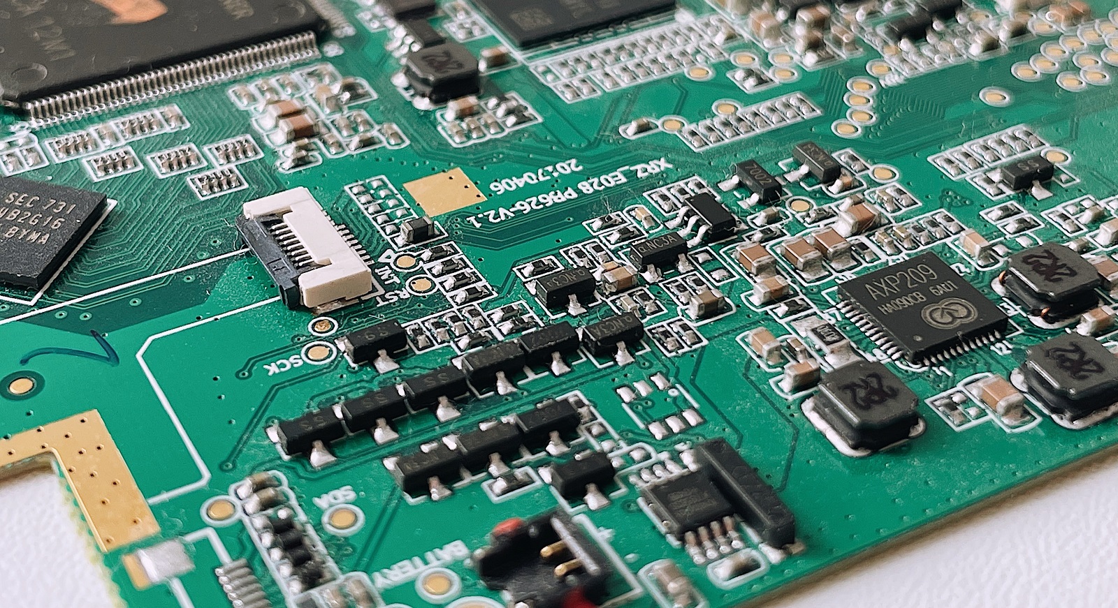
How a Remote Control Car Circuit Board Manages Motor Drive, Power, and Signal Control?
The remote control car circuit board acts as the central hub, integrating three critical subsystems.
| Subsystem | Key Components | Main Function |
|---|---|---|
| Signal Control | MCU, RF/IR Receiver | Signal decoding and PWM control |
| Motor Drive | H-Bridge, Driver IC | High-current motor speed and direction control |
| Power Management | Regulator, Capacitors, Battery Port | Voltage regulation for logic and RF circuits |
Design Logic: The PCB layout physically separates the “noisy” motor drive section (high current, fast switching) from the “quiet” signal control section (sensitive analog/digital lines). This is achieved through distinct power planes, strategic component placement, and liberal use of decoupling capacitors near ICs to prevent noise from causing erratic behavior.
Comparing Infrared and RF Solutions in an IR Remote Control Circuit for RC Cars
Choosing between Infrared (IR) and Radio Frequency (RF) defines the core performance of your simple remote control circuit.
- Infrared (IR) Remote Control Circuit:
- Principle: Uses modulated beams of infrared light (like a TV remote).
- Pros: Very low cost, simple IR remote control circuit diagram, lightweight components.
- Cons: Requires line-of-sight, short range (typically <10m), susceptible to interference from ambient IR sources (sunlight).
- Best For: Low-cost, indoor, or very short-range toy cars.
- Radio Frequency (RF) Remote Control Circuit:
- Principle: Uses specific radio bands (e.g., 2.4GHz, 27MHz, 49MHz) to transmit digital data.
- Pros: Long range (100m+), penetrates obstacles (non-line-of-sight), supports multiple channels and advanced protocols (like FHSS for interference avoidance).
- Cons: Higher cost and complexity than IR, requires FCC/CE certification.
- Best For: Virtually all hobbyist and professional-grade RC cars where reliable control is paramount.
For a reliable remote control car circuit, 2.4GHz RF technology is the definitive choice, making an ir remote control circuit suitable only for basic toy applications.
Design Logic Behind an RF Remote Control Circuit Diagram for Wireless Car Control
A robust RF remote control circuit diagram is architected for clarity, noise immunity, and efficiency. Key design pillars include:
- Modular Design: Use pre-certified RF transmitter and receiver modules. This simplifies design, reduces time-to-market, and ensures regulatory compliance.
- Stable Power Rails: Implement separate voltage regulators for the RF module and the digital logic. A noisy digital supply can severely degrade receiver sensitivity.
- Impedance Control & Grounding: For 2.4GHz designs, maintain controlled impedance for RF transmission lines. Use a solid, uninterrupted ground plane as a reference and shield.
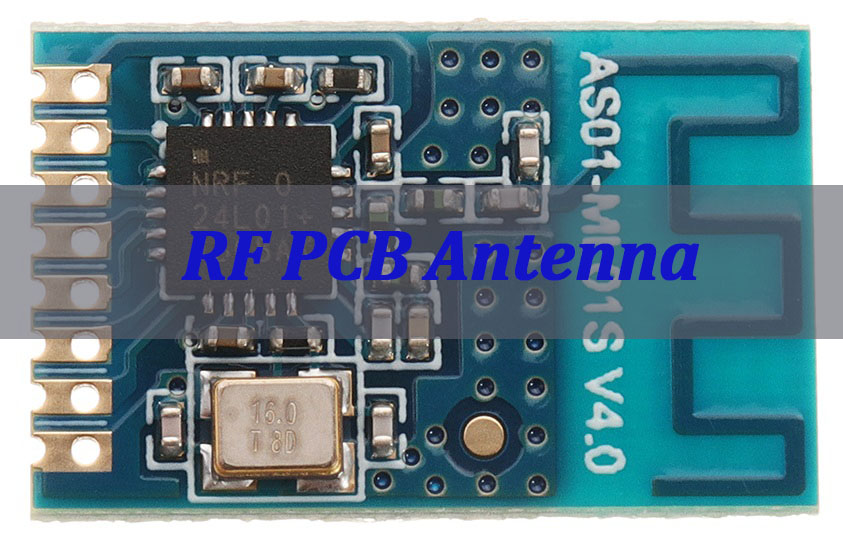
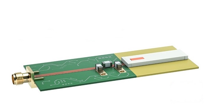
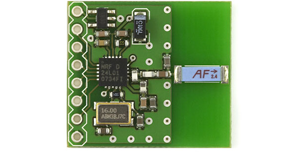
- Antenna Integration: Clearly define the antenna layout—whether it’s a printed trace, a ceramic chip antenna, or a connector for an external whip. Keep the antenna area clear of ground pour and noisy components.
- Signal Isolation: Route high-speed digital lines (from the MCU to the RF module) away from the antenna and keep them short. Use a filter on the power input to the RF module.
The goal is to translate a functional schematic into a PCB layout that preserves the integrity of the wireless signal from the transmitter IC to the antenna and back.
Where Is a Remote Controlled Circuit Commonly Used in Modern Electronics?
Beyond the thrilling world of RC cars, the principles of the remote control circuit are ubiquitous in modern technology. Its application is anywhere wired control is inconvenient, dangerous, or impossible.
- Consumer Electronics: TV remotes (IR), wireless speakers, smart home devices (RF).
- Industrial & Automation: Remote control circuit breaker for safe power disconnection, crane controls, agricultural machinery.
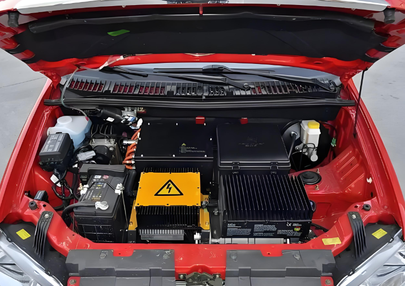
- Automotive: Keyless entry systems, tire pressure monitoring systems (TPMS).
- Aerospace & Defense: Drone/UAV control, remote control circuit breaker aircraft systems.
- Medical: Remote controls for hospital bed adjustments and diagnostic equipment.
The remote control circuit board is a foundational technology that enables the wireless interaction we increasingly take for granted.
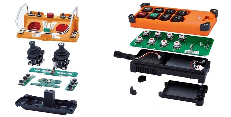
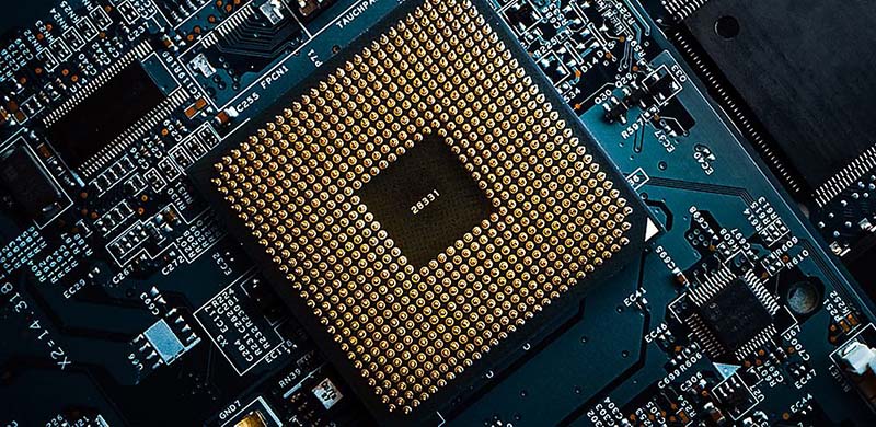
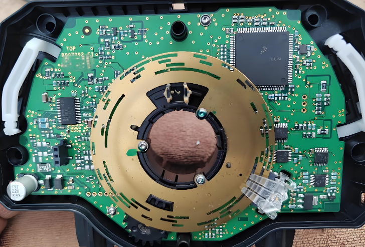
Key Components Used in a Circuit Board for Remote Control Car Applications
A reliable circuit board for remote control car integrates several key components, each with a specific role. Understanding these is crucial for both design and troubleshooting.
- Microcontroller Unit (MCU): The brain. It reads receiver signals, implements control logic, and generates PWM outputs for motors and servos.
- RF Transceiver Module: The communicator. A pre-built module (e.g., using nRF24L01+ or CC2500 chips) handles all complex RF transmission and reception, simplifying design.
- Electronic Speed Controller (ESC): The muscle driver. It takes a PWM signal from the MCU and drives the high-current brushless or brushed motor with the correct power and timing.
- Voltage Regulator: The power stabilizer. Steps down the main battery voltage (e.g., 7.4V) to clean 5V or 3.3V required by the MCU, receiver, and servos.
- Crystal Oscillator: The heartbeat. Provides the precise clock signal for the MCU and RF module to ensure stable operation.
- Passive Components: Resistors, capacitors, and inductors. They are used for filtering noise, setting bias points, and decoupling power supplies across the board.
What Role Does RF Technology Play in a Remote Controlled Circuit?
RF technology is the enabler of robust, real-time wireless control. Its role is multifaceted:
- Creating the Control Link: It provides the “invisible wire” that carries command data from transmitter to receiver over useful distances.
- Ensuring Reliability: Modern 2.4GHz systems use techniques like Frequency Hopping Spread Spectrum (FHSS) to automatically jump between frequencies, avoiding interference from other devices (Wi-Fi, other RC cars) and ensuring a stable link.
- Enabling Advanced Features: The digital data packets of RF systems can carry not just control signals but also telemetry data (like battery voltage, motor temperature) from the car back to the transmitter, enabling smart features and diagnostics.
- Supporting Scalability: 2.4GHz protocols allow binding of specific transmitters and receivers, enabling multiple cars to operate simultaneously without cross-interference, which is essential for racing.
In short, RF technology transforms a basic remote control circuit from a simple, interference-prone link into a sophisticated, reliable communication channel.
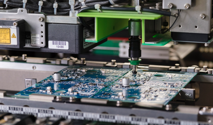
Why Choose EBest Circuit (Best Technology) for Remote Control Car PCB Circuit in Volume Production?
Scaling a prototype into thousands of reliable units requires a manufacturing specialist. BEST Technology is the ideal partner for your remote control car PCB circuit volume production because we focus on the specifics that matter for RC electronics.
- Design for Manufacturing (DFM) Expertise: We review your remote control circuit diagram and PCB files to suggest optimizations for yield, cost, and reliability before production begins.
- Material Sourcing & Management: We secure high-quality, consistent FR-4 laminates and components, ensuring every batch of your remote control car circuit board performs identically.
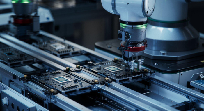
- Advanced Assembly Lines: Our automated SMT (Surface Mount Technology) lines accurately place tiny components (like 0402 resistors or QFN-packaged MCUs) critical for compact RC designs.
- Rigorous Testing Protocols: We implement in-circuit testing (ICT) and functional testing to verify that every board powers up, communicates via RF, and responds to inputs correctly.
- Conformal Coating Services: We offer professional coating application to protect boards from dust, moisture, and vibration—key for RC cars used in diverse environments.
- Supply Chain & Logistics Support: We manage the entire production flow, from procurement to assembly, testing, and final shipment, providing a single point of contact and responsibility.
Choosing BEST Technology means partnering with a factory that understands that a remote control car PCB circuit isn’t just a board; it’s the heart of your product, and we treat it with the precision and care it deserves.

In conclusion, remote controlled circuit design is the foundation of reliable, responsive, and scalable RC car electronics. This article has explored the core principles, components, and design considerations behind creating reliable wireless control systems for RC applications. From selecting the right materials and protocols to understanding the intricacies of PCB layout and volume manufacturing, each step is crucial for achieving a robust final product.
By combining RF-focused PCB engineering, advanced HDI manufacturing, and automated SMT assembly, EBest Circuit (Best Technology) enables remote controlled circuit designs to scale from prototype to stable mass production with controlled cost, quality consistency, and reliable performance. Pls feel free to contact our team at sales@bestpcbs.com to discuss your project.