PCB for USB chargers is the critical component that ensures safe and efficient energy transfer, powering everything from smartphones to tablets. Without a high-quality PCB, USB chargers would struggle to provide consistent performance or meet safety standards. In this blog, we’ll explore the importance of PCBs in USB chargers, how to choose the right design, and the benefits they bring to modern charging solutions. EBest Circuit (Best Technology), a leading PCB manufacturer in China, offers top-tier solutions tailored to the needs of reliable USB chargers.
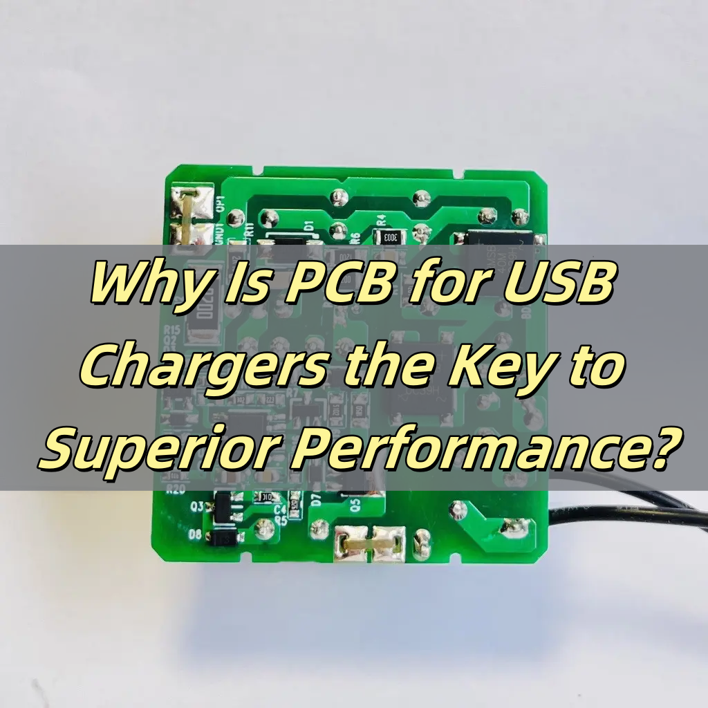
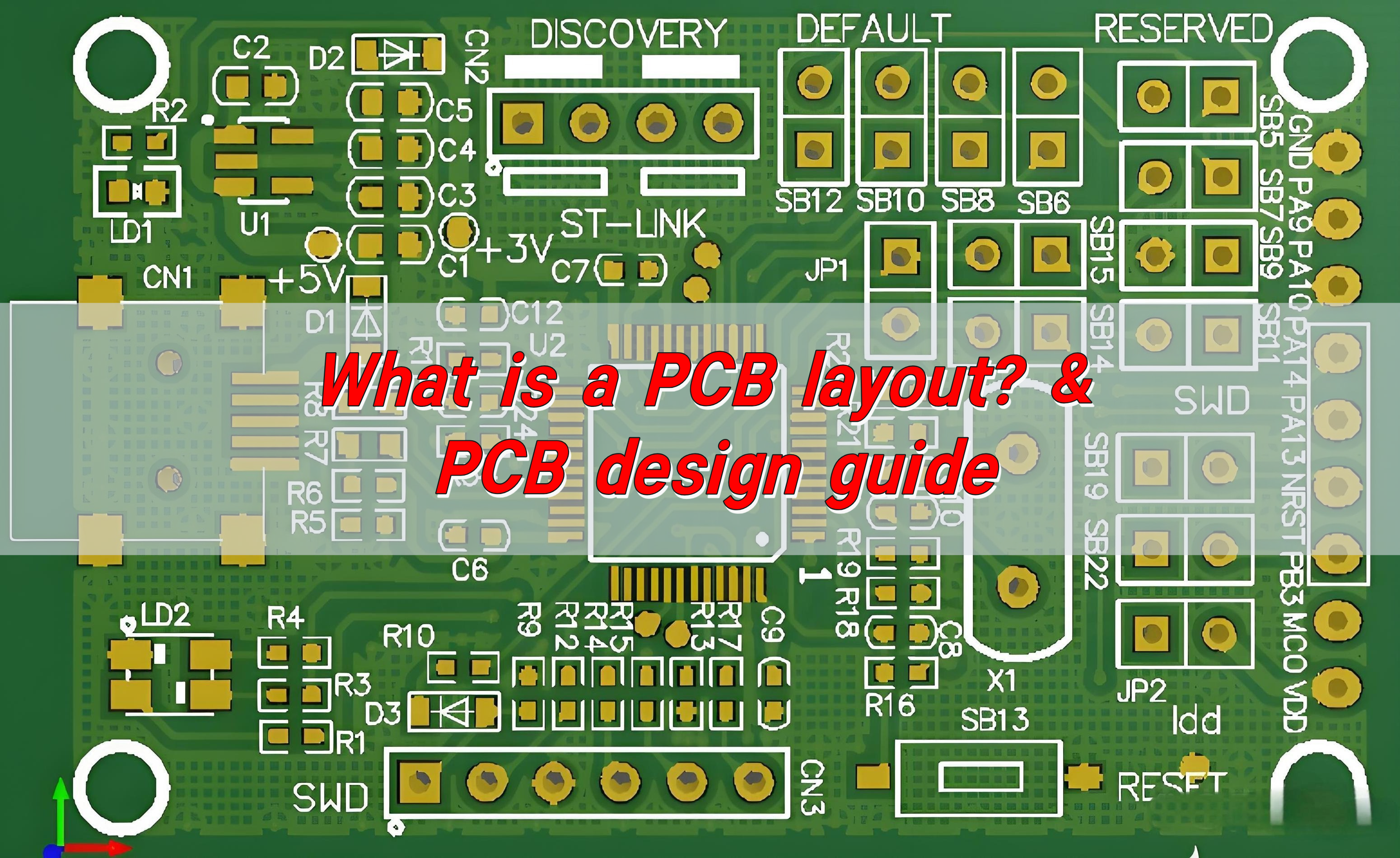
What Is PCB for USB Chargers?
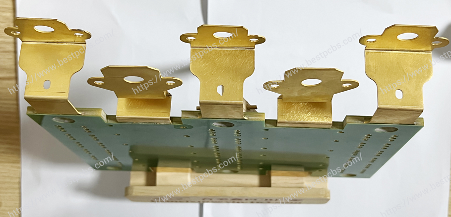
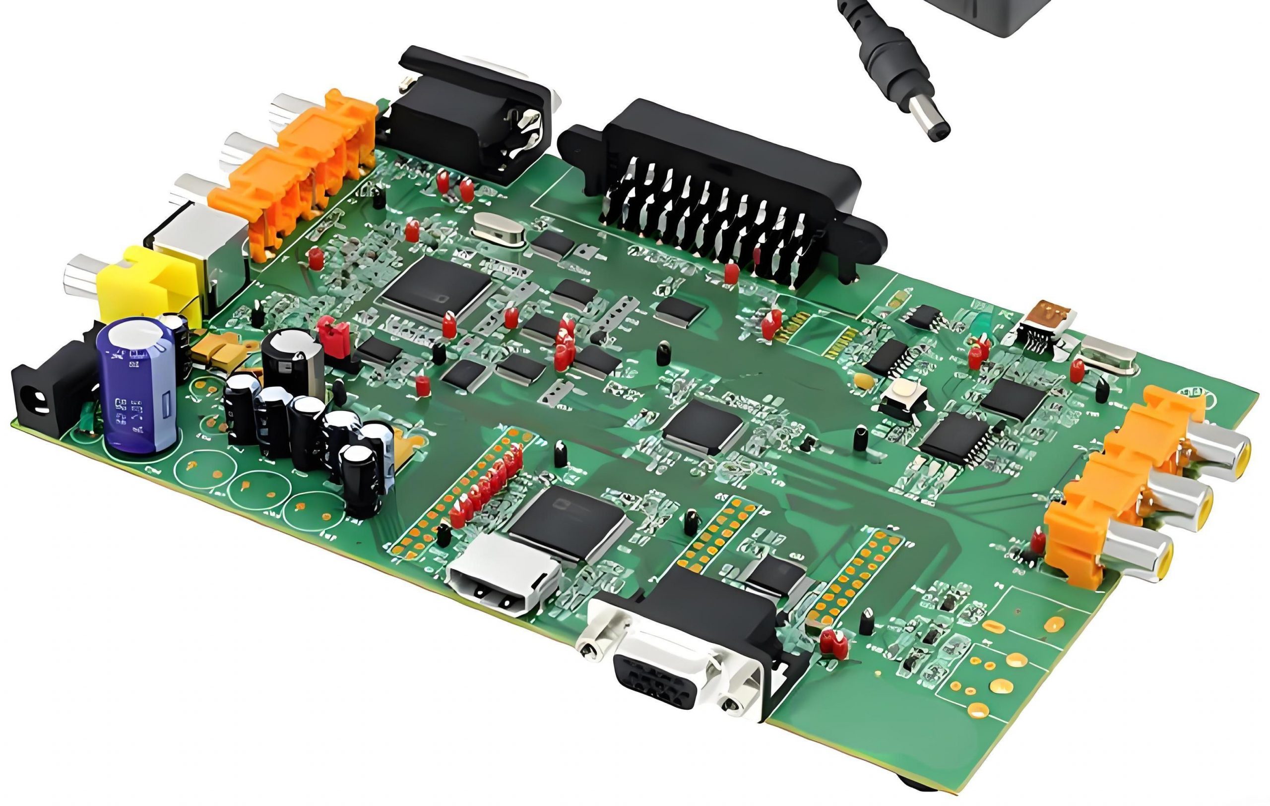
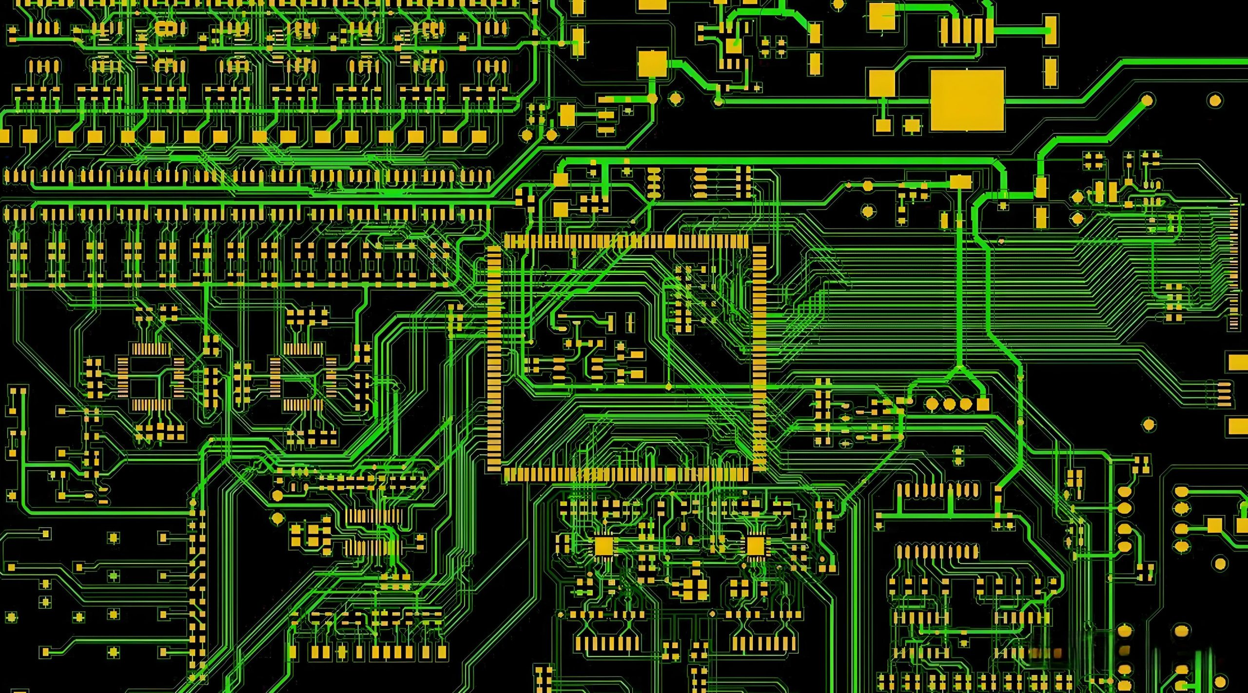
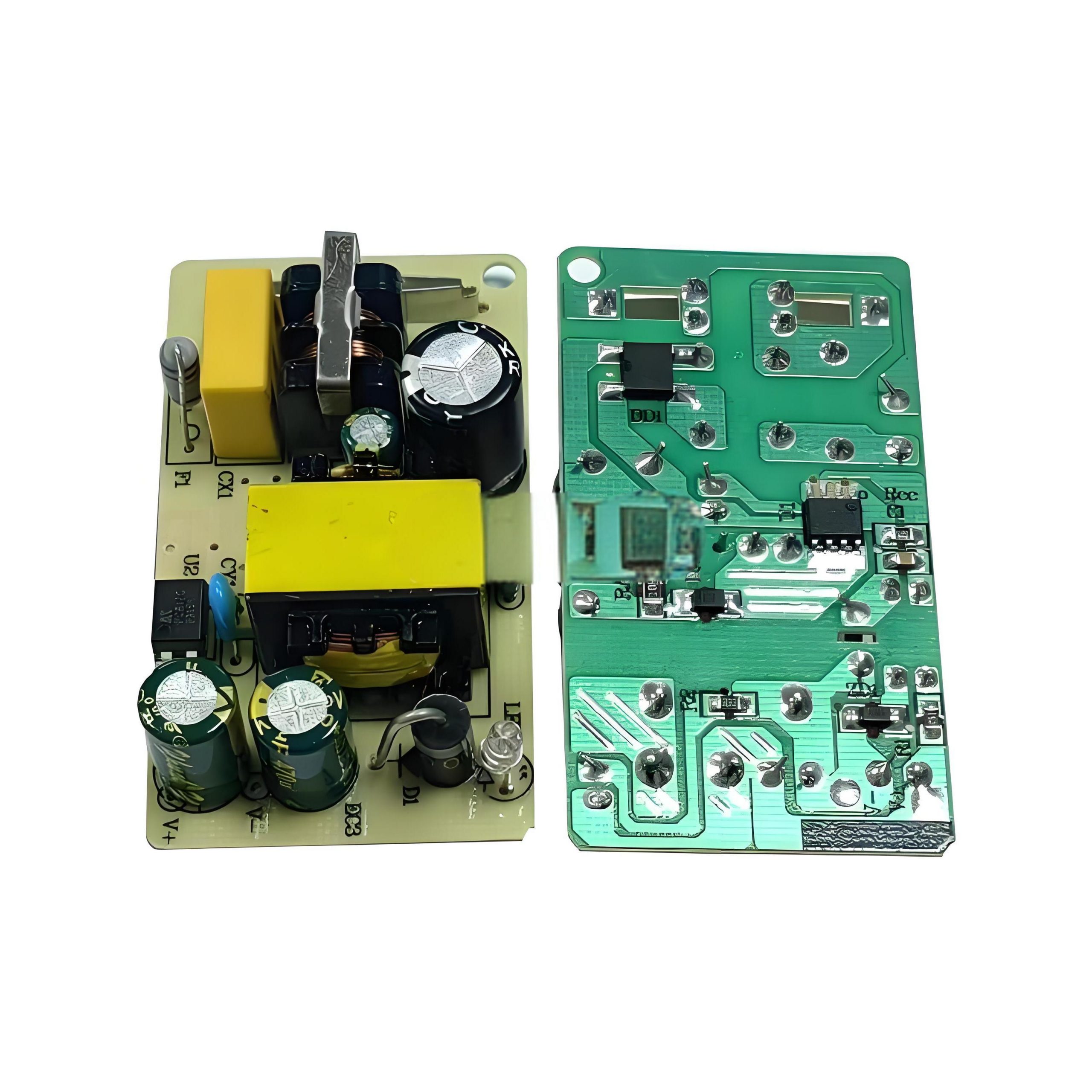
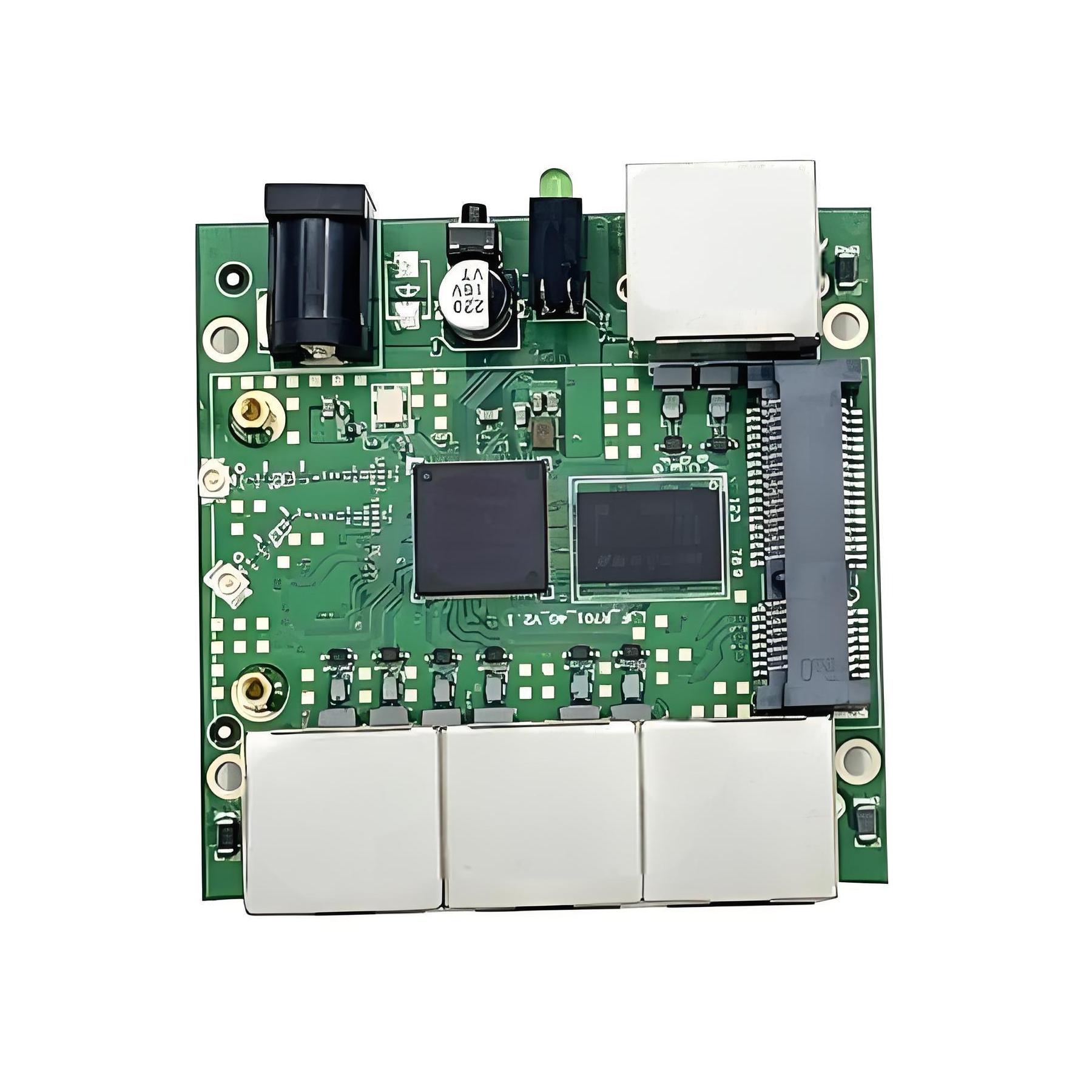
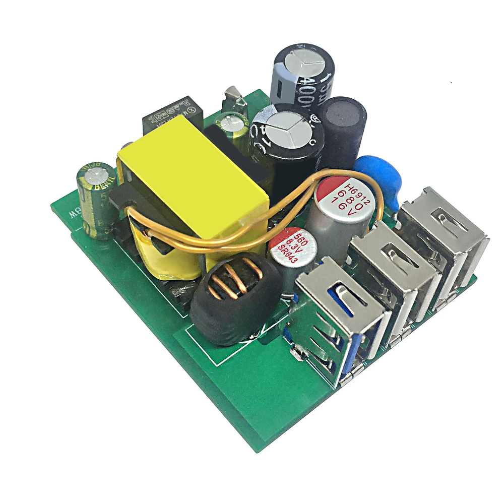
A PCB for USB chargers is the foundational component that controls the flow of electricity to charge devices. It serves as the backbone, hosting components like capacitors, resistors, and diodes. The PCB regulates voltage, ensuring devices receive the right amount of power without overheating or damaging sensitive electronics.
These boards are specifically designed to handle compact yet powerful circuits, making them ideal for USB chargers. Without the PCB, chargers would fail to deliver consistent and safe energy.
How to Choose the Right PCB Design for a USB Charger?
Selecting the right PCB design depends on several factors. Start by assessing the power requirements of the charger. Higher power outputs require PCBs with robust thermal management and reliable components.
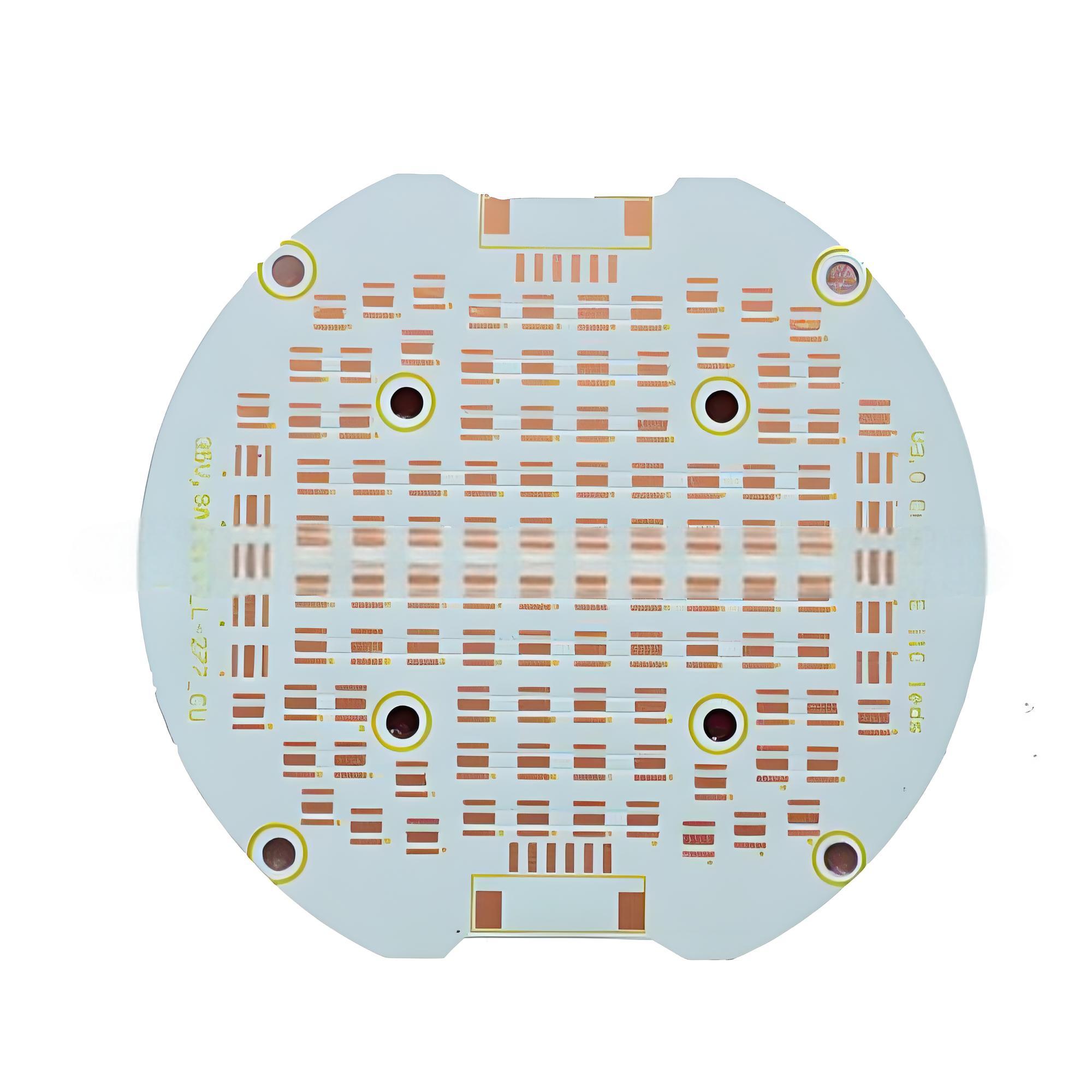
Next, consider the size of the PCB. USB chargers are compact, so the design must optimize space without sacrificing efficiency. Materials are another critical factor. High-quality substrates, such as FR-4, enhance durability and performance.
Finally, ensure the design complies with safety standards, such as CE and UL certifications. A well-designed PCB not only boosts functionality but also ensures user safety.
What Are the Common Issues with PCBs in USB Chargers?
While PCBs for USB chargers are highly efficient, a few issues can arise if not designed or manufactured correctly. Overheating is one of the most common problems, often caused by poor thermal management or low-quality materials.
Component failure, such as damaged capacitors or resistors, can disrupt the charging process. Additionally, improper soldering may lead to connection failures. However, choosing a reliable manufacturer minimizes these risks, ensuring long-lasting performance.
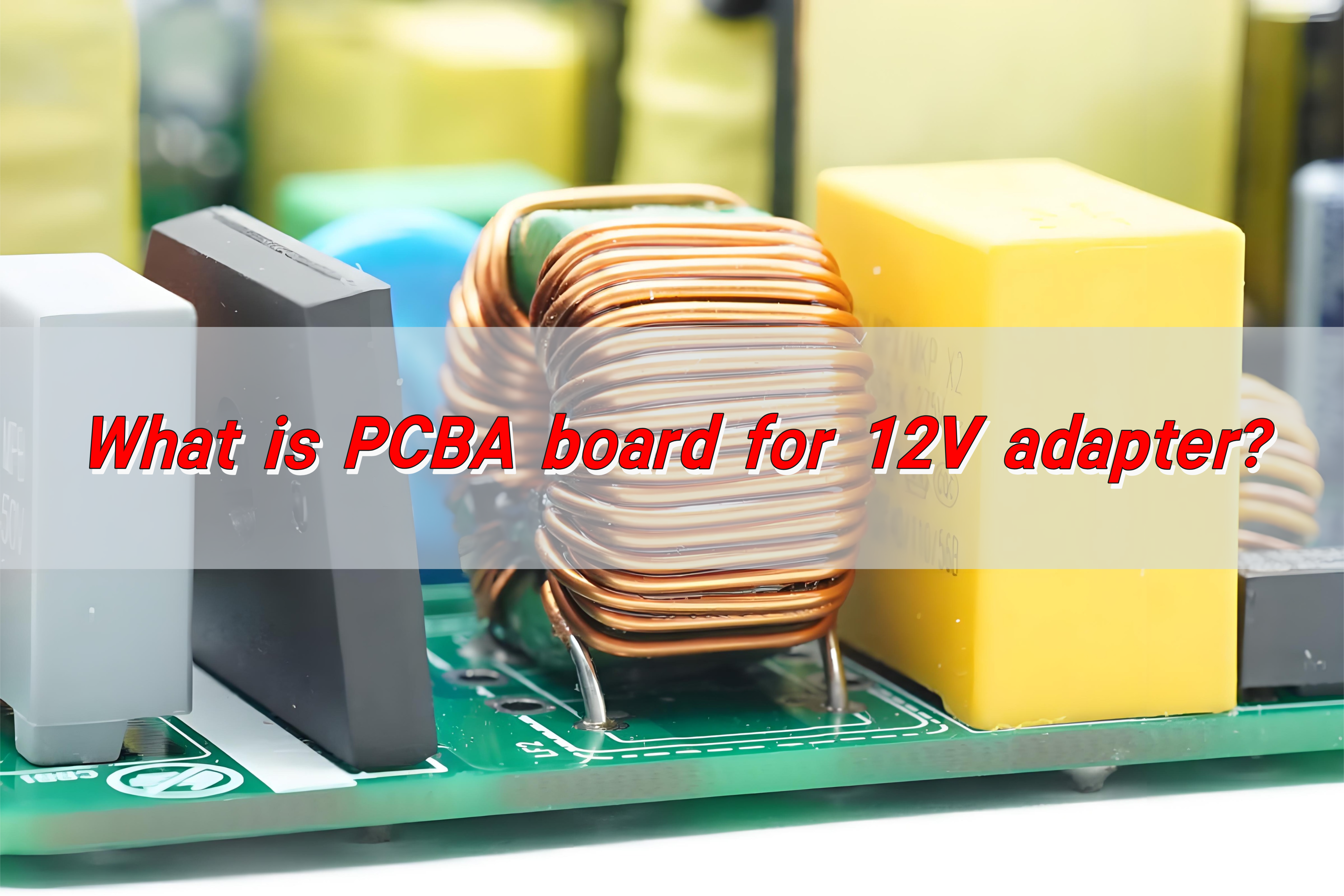
Why Is Thermal Management Important in USB Charger PCBs?
Thermal management is critical for the safety and efficiency of USB charger PCBs. As the board regulates voltage, it generates heat. Without proper heat dissipation, components can overheat, reducing the lifespan of the charger.
Effective thermal management involves using heat-resistant materials and incorporating heat sinks or thermal vias. These measures prevent overheating, ensuring that the PCB operates safely and consistently even under heavy usage.
What Is the Cost of Designing and Manufacturing a PCB for USB Chargers?
The cost of designing and manufacturing a PCB for USB chargers varies based on complexity, materials, and volume. High-quality PCBs typically cost more upfront but deliver better durability and performance.
Custom designs tailored to specific needs may increase costs slightly but provide superior functionality. Partnering with experienced manufacturers ensures a balance between affordability and quality, making it easier to produce reliable chargers.
How to Ensure Safety in USB Charger PCB Design?
Safety is a top priority in PCB design for USB chargers. Start by using high-quality materials that can handle high temperatures and electrical loads. Incorporate protective components such as fuses and surge protectors to guard against electrical faults.
Proper insulation and spacing between components also reduce the risk of short circuits. Testing is essential. Ensure each PCB undergoes rigorous quality checks to comply with industry standards. A safety-first approach builds trust and enhances the user experience.
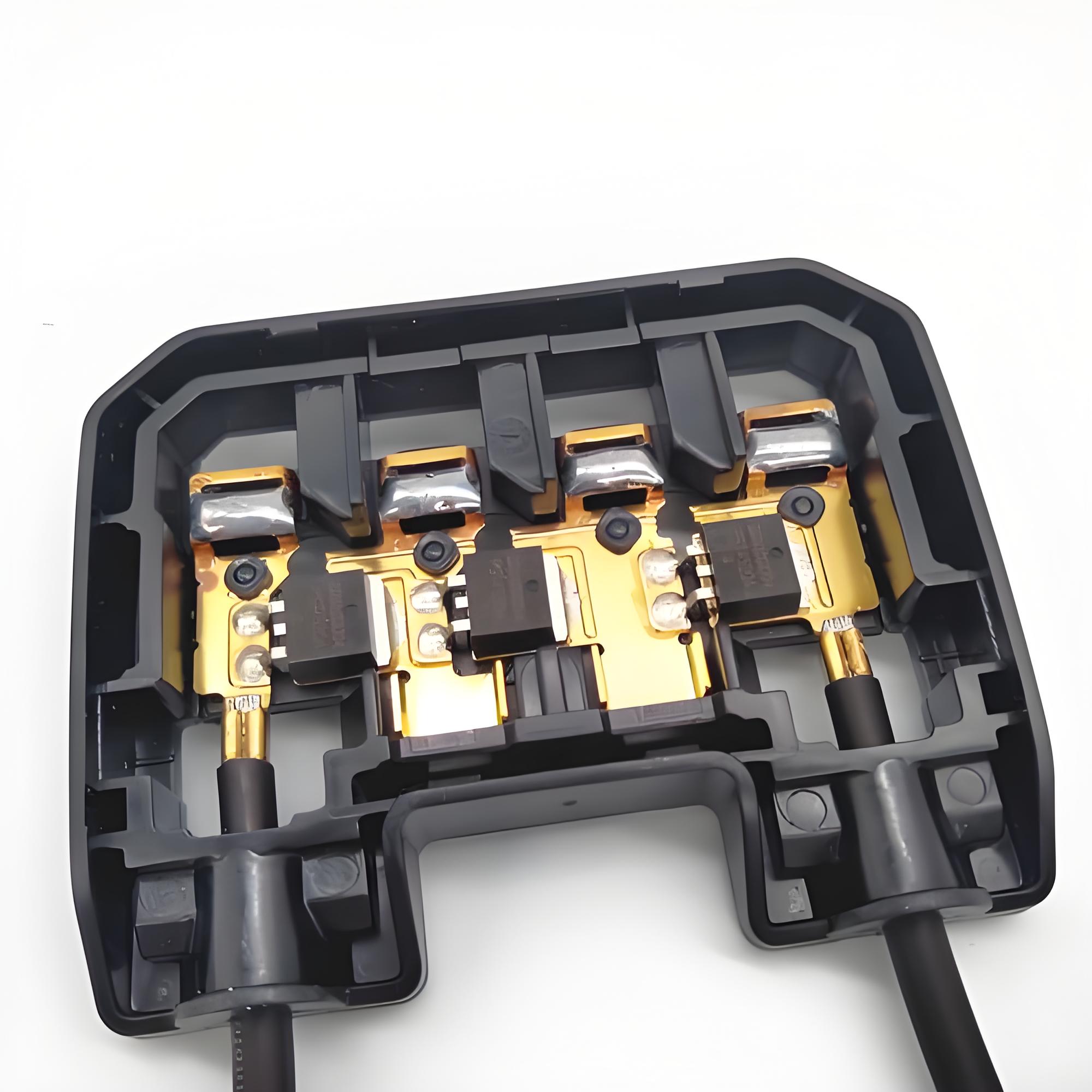
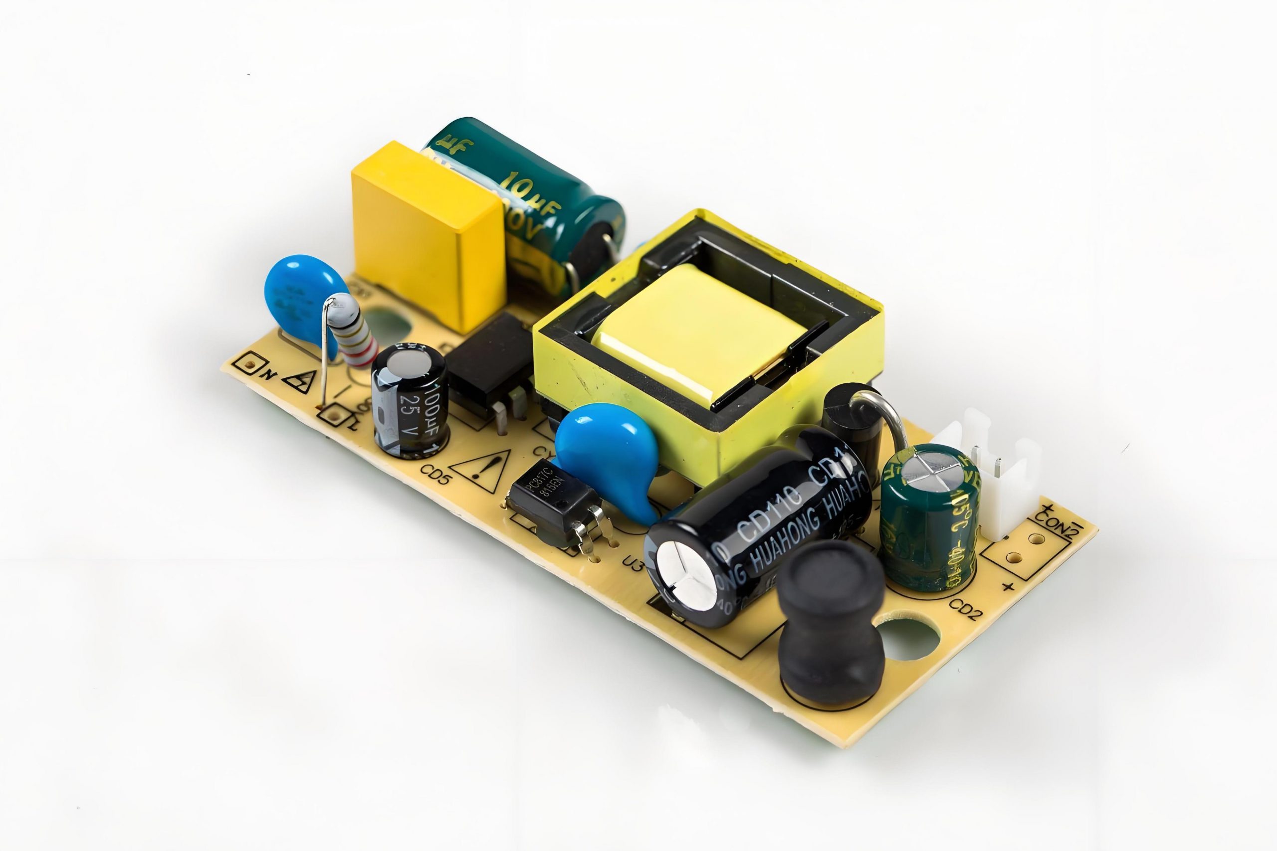
How Does the PCB in a USB Charger Work?
The PCB in a USB charger works as the control center, regulating the flow of electricity from the power source to the connected device. It converts high-voltage AC power to low-voltage DC power suitable for charging.
Voltage regulators, resistors, and capacitors on the PCB work together to stabilize the current. These components protect devices from power surges, ensuring safe and efficient charging. The compact design of PCBs allows USB chargers to deliver powerful performance without compromising portability.
What Are the Benefits of Using a High-Quality PCB for USB Chargers?
High-quality PCBs offer several advantages. They enhance the performance and reliability of USB chargers, ensuring faster and safer charging. Durable materials and precise designs reduce the risk of overheating and component failure.
Additionally, high-quality PCBs improve energy efficiency, minimizing power loss during operation. By choosing premium PCBs, manufacturers can create chargers that meet customer expectations while adhering to global safety standards.
PCBs are the unsung heroes behind the seamless performance of USB chargers. From ensuring safety to enhancing efficiency, they play a vital role in modern charging solutions. By selecting high-quality designs and partnering with trusted manufacturers like EBest Circuit (Best Technology), businesses can deliver reliable, safe, and efficient chargers to their customers.
Whether you’re designing USB chargers or sourcing components, investing in high-quality PCB for USB chargers ensures better performance and customer satisfaction. Choose EBest Circuit (Best Technology), your trusted PCB manufacturer in China, to experience superior quality and service.