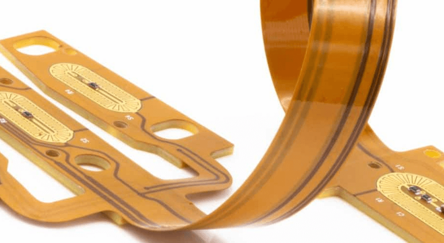
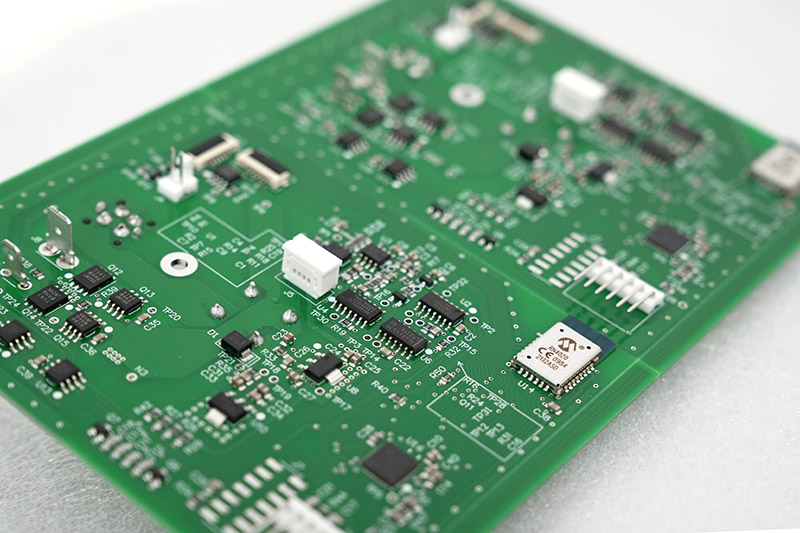
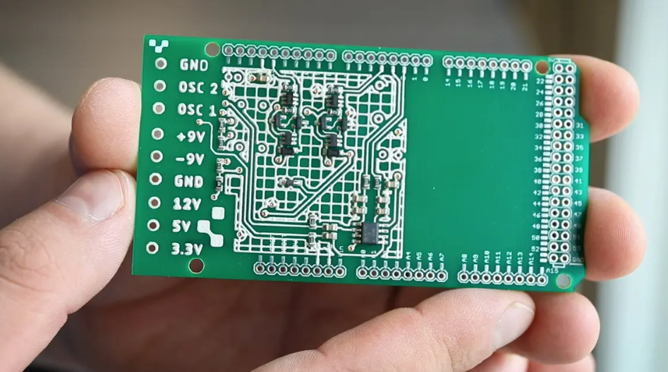
High frequency circuit board is a PCB built to handle signals that move at very high speeds with minimal loss. It uses special materials that keep signals stable, even when the frequency rises. These materials help reduce noise, keep impedance steady, and maintain strong signal integrity.
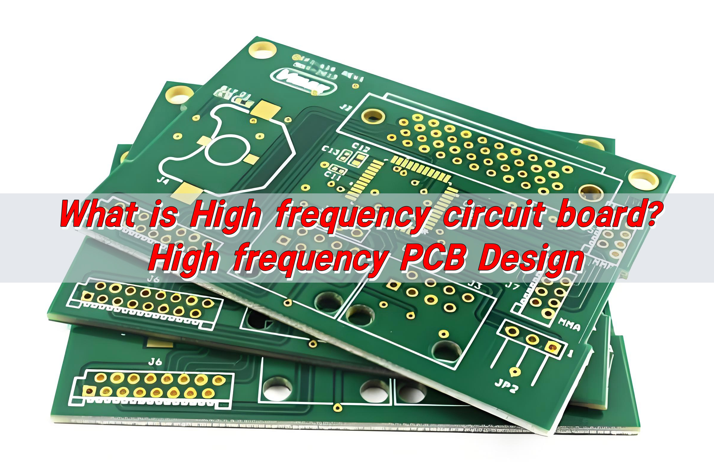
What Is a High-Frequency PCB?
A high frequency circuit board, sometimes called a high frequency printed circuit board, is a board made to carry signals at very high speeds. These signals often run above 500 MHz and can climb to several GHz.
That means the board must offer tight control, low loss, and stable performance even when the signal moves at extreme velocity. In simple terms: A high frequency PCB helps a device talk fast, respond fast, and stay accurate.
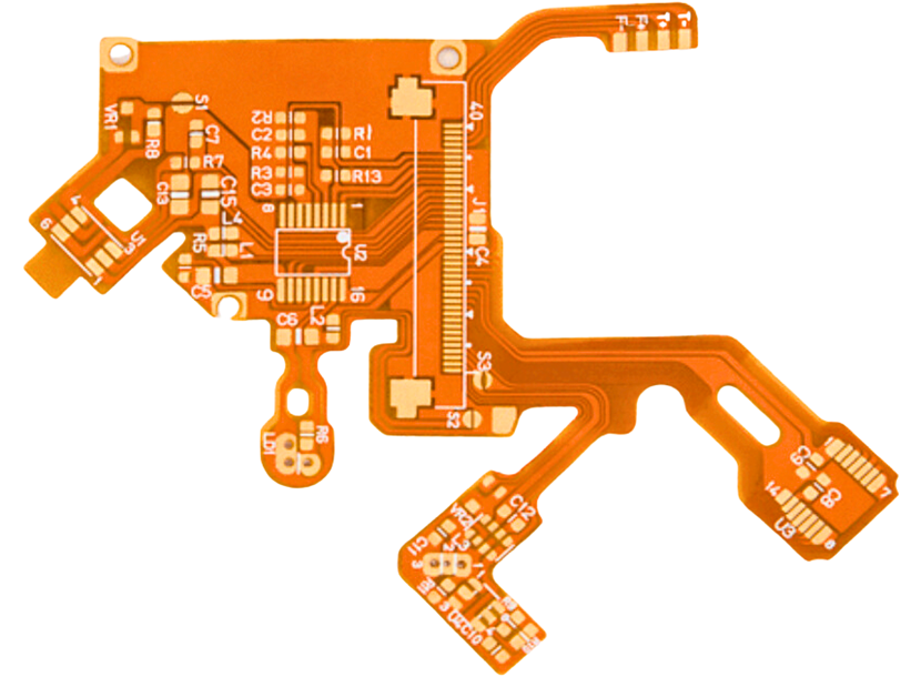
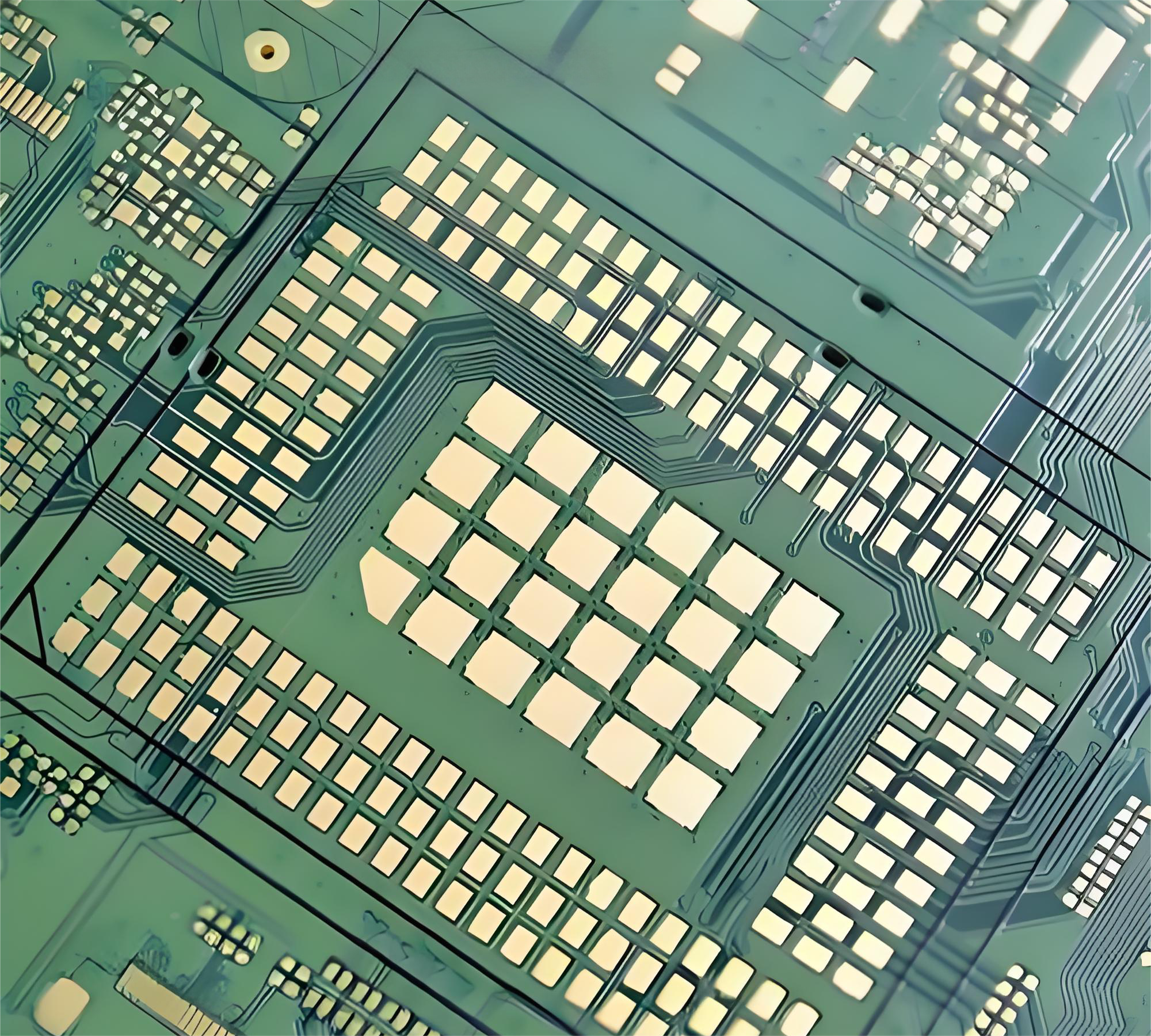
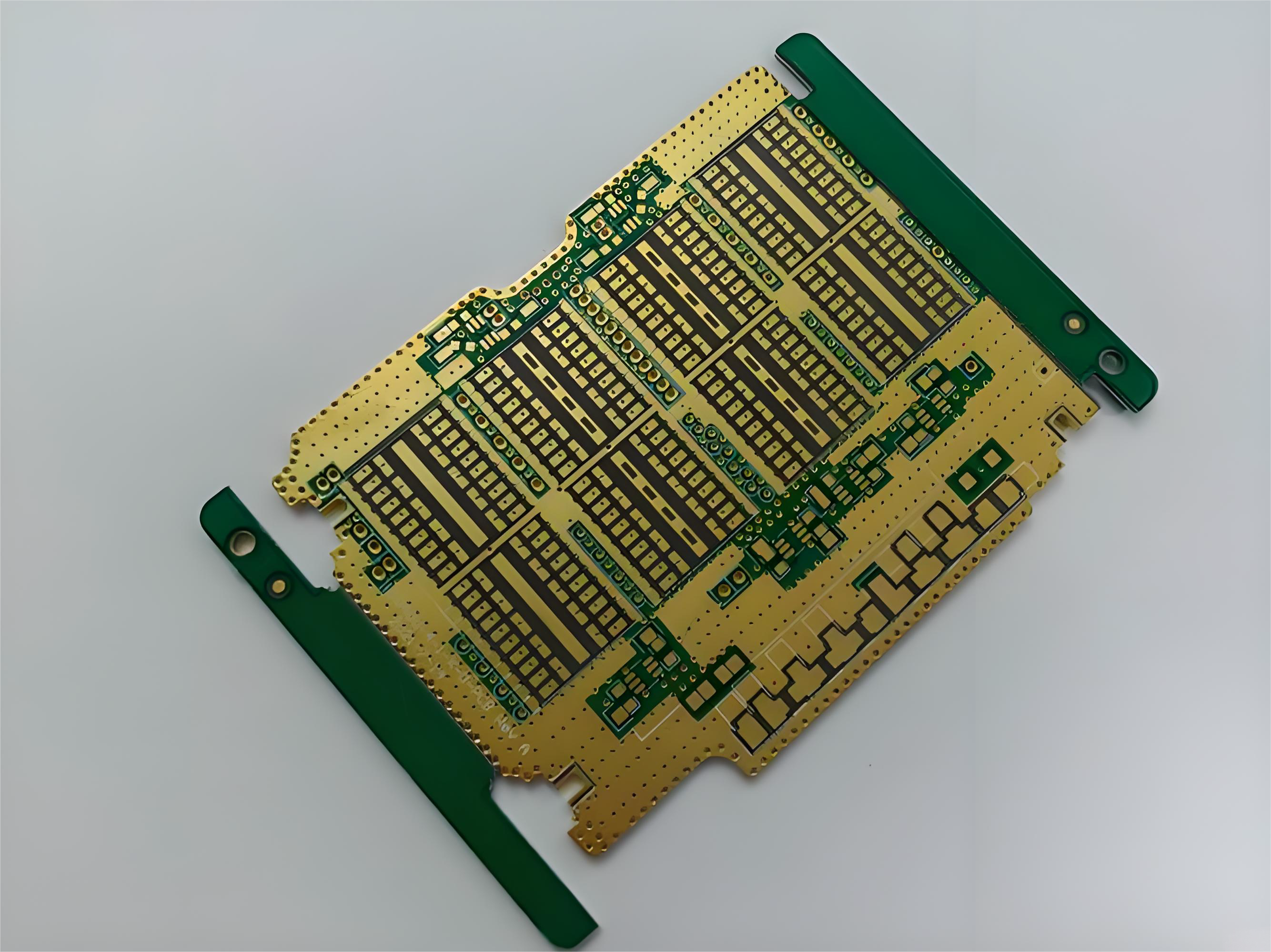
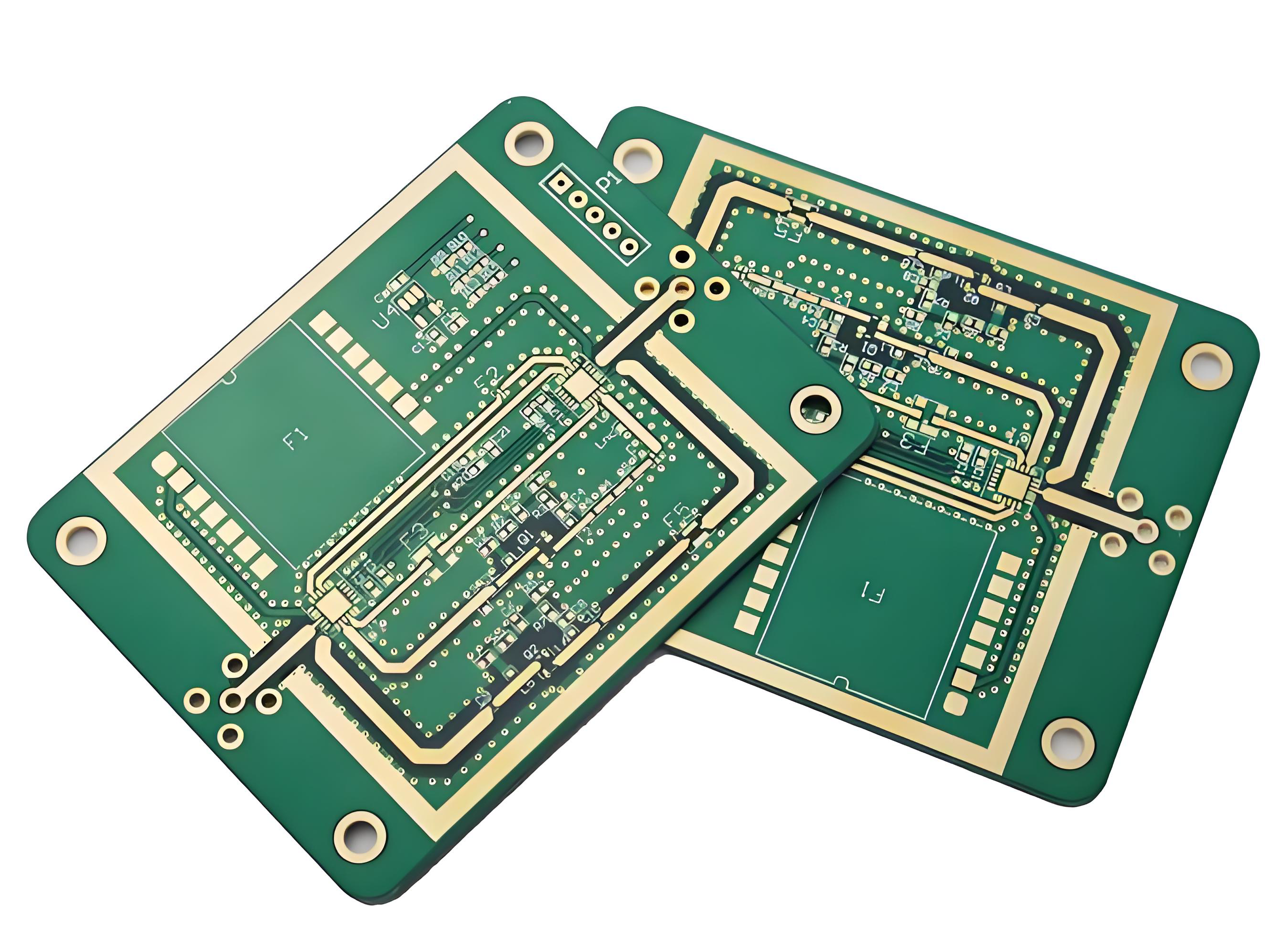
The layout, the copper, the materials, and even tiny distances all matter more here than on standard boards. Every trace acts like a small transmission line. Every layer impacts performance.
Because of this, these boards follow strict high frequency PCB design guidelines to keep everything stable.
What Are the Advantages of High Frequency Circuit Boards?
High frequency boards bring real-world advantages that normal boards can’t offer. If you need to transfer data quickly and keep it accurate, then you can choose this.
- They Deliver Faster, Cleaner Signals
High-frequency signals can be delicate. They hate distortion. They hate delay. A high frequency board keeps signals clean even at high speed. This helps products work with precision and smooth flow.
- They Offer Strong Performance Stability
High frequency materials stay stable even when temperatures shift. This leads to reliable data flow, fewer losses, and greater accuracy.
- They Support High-Quality Wireless Performance
WiFi, radar, GPS, and 5G all rely on clean high-frequency signals. A high frequency PCB handles these signals without breaking a sweat.
- They Enable Slim, Compact Designs
Better materials and tighter control allow compact layouts. This makes devices smaller, lighter, and more stylish. They Improve Power Efficiency
Lower loss means better conversion and lower waste. The device stays cool and runs longer.
These advantages feel small one by one, but together, they create a powerful boost across the entire system.
Which High Frequency PCB Materials Work Best?
Materials are the heart of performance for a high frequency board. In fact, everyone believes that material selection is the primary decision that determines everything else.
Why Material Matters So Much?
High-frequency signals react to even tiny changes in dielectric properties. If the material is unstable, the signal weakens. If the material is too lossy, the device feels slow. If the material varies with temperature, the system becomes unreliable.
Most Popular Options
- PTFE-Based Materials: These are common in high-end RF and microwave designs. They offer low loss and stable dielectric values. They also work well with GHz-level signals.
- Ceramic-Filled Materials: These deliver excellent thermal stability. They support consistent performance across temperatures.
- Hydrocarbon-Based Materials: These offer good performance but are easier to fabricate than PTFE. Great for designs that need both quality and reasonable cost.
- Modified Epoxy Systems: These are good for mid-frequency applications. They work well for cost-sensitive projects that still need solid stability.
Each material fits a different level of performance and budget. The “best” one depends on speed, cost, thermal needs, size, and end-use demands.
How Does a High-Frequency Circuit Differ From a Standard PCB?
The difference between high-frequency circuits and standard PCBs is significant. They may look similar at first glance, but their internal structures are completely different.
Key Differences
- 1. Material Characteristics
Standard FR4 does not offer stable performance at high frequencies. It cannot maintain low loss or tight impedance at high speeds. High frequency PCBs use advanced materials that keep everything stable.
- 2. Signal Integrity Requirements
A standard PCB tolerates more variation in length and width. A high frequency circuit cannot. Even small changes can shift impedance and distort the signal.
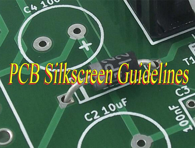
- 3. Stricter Design Rules
High frequency PCB design follows guidelines for trace width, spacing, ground layout, and layer stack. Standard PCBs are more flexible.
- 4. Tighter Manufacturing Tolerances
A tiny shift in etching can affect performance. So fabrication must be more accurate.
- 5. More Sensitive Thermal Behavior
High frequency materials react more predictably to heat. This adds stability during real-world use.
In short, high frequency boards are built for speed, clarity, and precision.
What Affects High Frequency PCB Performance?
High frequency performance depends on a chain of factors. One weak link affects the whole system. Here are the main forces that steer performance.
- 1. Dielectric Constant (Dk)
The dielectric constant shapes how signals travel through the board. If Dk is unstable, the signal wobbles. A steady Dk makes the circuit feel sharp, clean, and fast.
- 2. Dissipation Factor (Df)
This controls energy loss. Lower Df means the signal stays clean and strong. Higher Df means more heat and weaker flow.
- 3. Copper Roughness
Smooth copper helps signals glide with less loss. Rough copper slows everything down.
- 4. Trace Width and Spacing
These shape impedance. Small changes can shift impedance and hurt signal quality.
- 5. Via Design and Placement
Each via adds inductance. Too many vias interrupt the path. Smart via design keeps the system balanced.
- 6. Layer Stack-Up Structure
Stack-up controls grounding, shielding, and loss. A good stack-up enhances signal flow.
- 7. Ground Layout
Ground shape and size guide return paths. Poor ground layout causes noise. Strong ground layout protects the signal.
- 8. Temperature Stability
High frequency boards must keep dielectric values steady across temperature changes.
These factors bring life to the entire system and shape how smoothly it performs.
What Are the Applications of High-Frequency PCBs?
High frequency PCBs show up everywhere today. They power advanced technologies that shape modern life. The following are their main application areas.
- 5G Telecommunications: 5G needs fast, stable, high-frequency signals. These boards make that possible.
- Satellite and Aerospace Systems: Navigation and communication systems rely on accurate RF circuits. High frequency boards offer stability under extreme conditions.
- Radar Systems: Vehicle radar, weather radar, and military radar all depend on precision. Only high frequency PCBs can handle the demands.
- Automotive Electronics: ADAS, blind spot systems, radar sensors, and infotainment systems rely on fast, clean signals.
- Medical Devices: MRI scanners, imaging systems, and mobile medical tools use high frequency signals.
- Consumer Electronics: WiFi routers, Bluetooth devices, smart home hubs, and high-speed wearables rely on these boards.
- Industrial Control Systems: Factories need accurate, fast data movement.
- IoT Systems: Smart sensors communicate at high frequencies to stay fast and efficient.
In each field, the board supports speed, accuracy, and reliability.
What Matters Most in High-Frequency Circuit Design?
High-frequency PCB design is extremely delicate. All components must work in harmony to achieve perfect balance. Here are some of the most important parts.
- Impedance Control: Impedance must stay consistent along every trace. This keeps reflection low and signal quality high.
- Return Path Design: A clean return path keeps noise low and improves clarity.
- Layer Stack Strategy: A stable stack sets the foundation for signal flow.
- Trace Routing: Shorter paths help signals move quickly. Smooth curves reduce reflection. Clean routing limits crosstalk.
- Material Selection: This affects loss, speed, temperature stability, and cost.
- Grounding and Shielding: Strong grounding protects signals from noise. Shielding helps maintain signal integrity.
- Controlled Transitions: Via transitions must stay smooth.
- Thermal Management: High frequency circuits generate heat.
These design choices protect the signal like a shield. They keep performance strong and predictable.
What Problems Often Occur in High Frequency PCB Design?
Despite the maturity of high-frequency PCB design technology, challenges remain. Most problems stem from the extremely high frequency sensitivity of signals. Below are some frequently encountered issues.
- 1. Signal Loss
Loss grows as frequency rises. If materials or copper are not ideal, performance drops.
- 2. Impedance Problems
Wrong trace width, copper changes, or bad stack-up cause impedance mismatch. Mismatch creates reflections.
- 3. Crosstalk
When traces sit too close, they talk to each other. This hurts accuracy.
- 4. Poor Via Design
Too many vias act like road bumps. They disrupt the signal flow.
- 5. Weak Ground Design
A poor ground path increases noise. Noise spreads across the system.
- 6. Thermal Drift
Temperature changes can shift dielectric constant. This affects timing and performance.
- 7. Fabrication Tolerance Issues
High frequency designs rely on tight tolerances. Even small etching errors can create problems.
- 8. Material Incompatibility
Some materials require special fabrication steps. If not handled correctly, results suffer.
Smart planning and strong guidelines help avoid these issues and keep performance at its best.
Conclusion:
High frequency circuit board plays a powerful role in modern electronics. It guides signals at high speed. It improves clarity. It boosts wireless strength.
If you need high-quality high-frequency PCB support or professional guidance, feel free to reach out anytime at: sales@bestpcbs.com