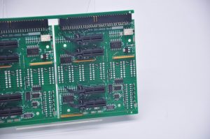
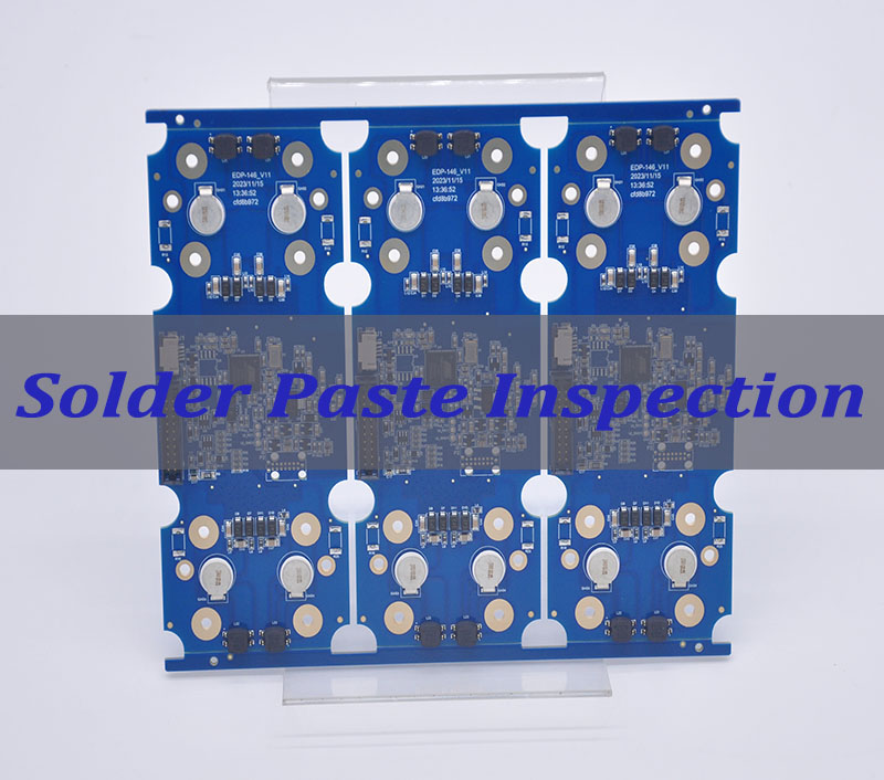
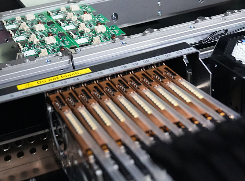
Solder paste inspection (SPI) is a critical quality control process in Surface Mount Technology (SMT) manufacturing that examines the quality, volume, and placement of solder paste post-printing and before component placement. This article delves into the technology, standards, and strategic importance of implementing professional solder paste inspection for achieving superior Printed Circuit Board Assembly (PCBA) reliability and yield.
Common PCBA Manufacturer Pain Points:
- Escaping Defects: Suffering from high rates of solder defects like bridging, insufficient paste, or misalignment that are only caught after reflow, leading to massive scrap and rework costs.
- Cost of Manual Checks: Relying on slow, error-prone, and subjective manual visual inspection under microscopes, which is unsustainable for high-volume production.
- Process Drift & Inconsistency: Struggling with uncontrolled variation in the printing process due to stencil wear, paste viscosity changes, or printer misalignment, causing unpredictable yield fluctuations.
- Micro-Components Challenge: Finding it impossible to reliably inspect ultra-fine-pitch components, 01005, or 0.3mm pitch BGA solder paste deposits with traditional 2D methods.
- Lack of Actionable Data: Operating without real-time, quantitative data to make informed process adjustments, leaving teams to make guesses based on post-reflow failures.
Transitioning to a closed-loop, data-driven SMT process control system starts with implementing a professional 3D solder paste inspection machine. This approach directly targets and resolves these core challenges.
Core Solutions for Superior Yield:
- Catch Defects at Source: A 3D solder paste inspection system identifies printing defects immediately after the stencil printer, preventing bad boards from proceeding down the line and eliminating costly post-reflow rework.
- Full Automation & Speed: Replaces slow manual checks with fast, objective, and repeatable automated optical inspection, achieving 100% inspection coverage at line speed.
- Real-Time Process Control: Continuously monitors key solder paste inspection parameters (height, area, volume) to detect process drift early, enabling timely correction before it impacts yield.
- High-Resolution 3D Measurement: Utilizes advanced 3D sensing technology (e.g., laser or phase-shift profilometry) to accurately measure the volume and shape of paste deposits for the smallest components, far beyond the capabilities of 2D solder paste inspection.
- Statistical Process Control (SPC) Data: Provides actionable, real-time SPC data and trend charts, empowering engineers to optimize printer settings, stencil design, and paste management for continuous process improvement.
At BEST Technology, we are a leading provider of advanced PCBA and ceramic PCB manufacturing solutions. We understand that superior assembly quality is built on a foundation of precise process control. Our expertise integrates industry-leading solder paste inspection equipment and best practices to ensure every product meets the highest reliability standards. For a partnership dedicated to achieving flawless yield, pls feel free to contact us at sales@bestpcbs.com.
What Is Solder Paste Inspection?
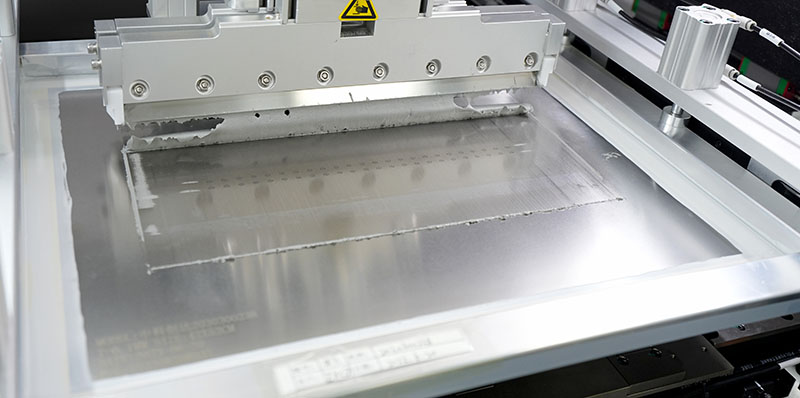
Solder Paste Inspection (SPI) is an automated, in-line quality control process performed immediately after the solder paste printing stage in SMT assembly. Its primary function is to verify the quality of the printed solder paste deposits on the PCB pads before components are placed. This proactive check is crucial because printing is the number one source of soldering defects. An effective solder paste inspection process measures critical attributes to ensure they fall within predefined solder paste inspection tolerance limits.
- Core Objectives of SPI:
- Defect Prevention: Identify printing errors early to prevent defective boards from undergoing expensive component placement and reflow.
- Process Monitoring: Provide quantitative feedback on the health and stability of the stencil printing process.
- Yield Improvement: Directly increase first-pass yield and reduce total cost of ownership by minimizing rework and scrap.
- Key Measured Parameters: A sophisticated 3D solder paste inspection machine typically measures the following for each paste deposit:
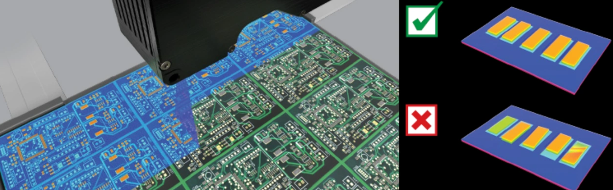
- Volume: The most critical parameter. Ensures there is enough solder to form a reliable joint but not so much as to cause bridging.
- Height/Thickness: Measures the paste deposit’s profile and peak height.
- Area & XY Alignment: Checks the coverage area and positional accuracy of the paste relative to the PCB pad.
- Shape & Bridge Checking: Analyzes the deposit’s shape profile and detects potential bridging between adjacent pads.
- 2D vs. 3D SPI: While basic 2D solder paste inspection can check for presence, alignment, and gross bridging, it cannot measure volume or height. 3D solder paste inspection technology is now the industry standard because it provides the volumetric data essential for modern, fine-pitch components. How does 3D solder paste inspection work? It typically uses laser triangulation or phase-shift moiré techniques to construct a precise three-dimensional map of the paste deposits.
In summary, solder paste inspection is the essential first gate in SMT quality control, transforming the printing process from a “black box” into a measured, controlled, and optimized step.
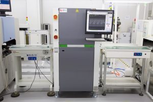
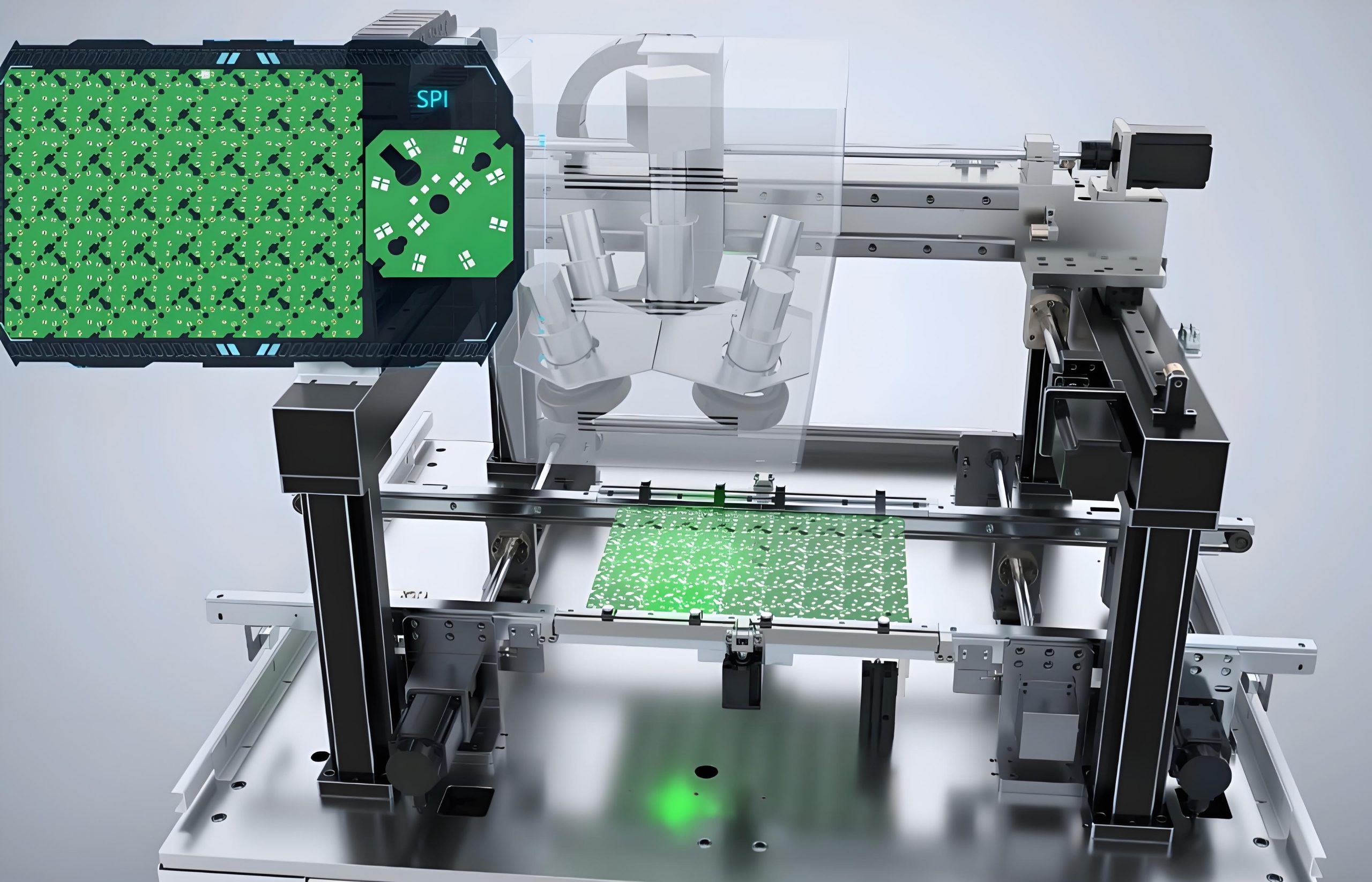
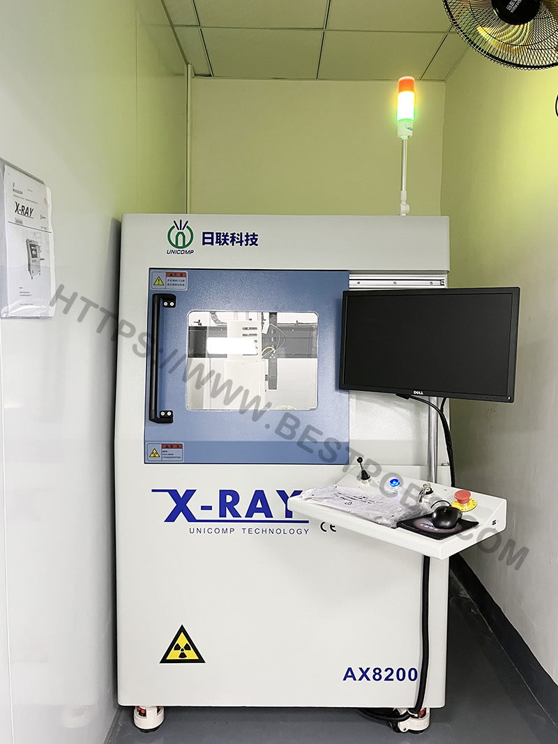
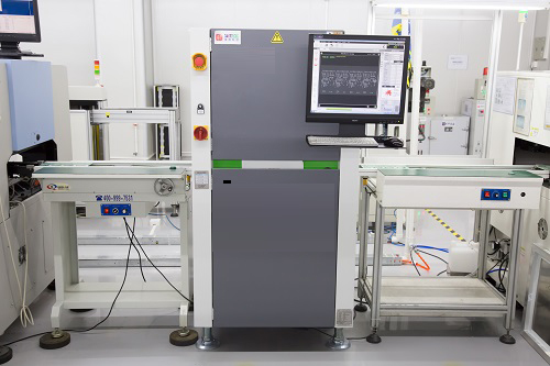
How Does 3D Solder Paste Inspection Work?
Understanding how does the solder paste inspection machine work demystifies its critical role. Modern 3D solder paste inspection systems operate at high speed with incredible precision, using non-contact optical methods to build a detailed height map of the entire PCB. The core technology enables the 3D solder paste inspection work to be both comprehensive and fast.
The process typically follows these steps:
- Board Alignment & Fiducial Recognition: The machine uses the PCB’s fiducial marks to precisely align the board under the inspection cameras, ensuring measurement accuracy.
- 3D Data Acquisition: A scanning mechanism moves across the board. The most common technologies are:
- Laser Triangulation: A laser line is projected onto the paste. A camera at a known angle captures the line’s deformation. The deformation is used to calculate height, constructing a 3D profile.
- Phase-Shift Profilometry (Moiré): Patterns of light are projected onto the surface. The distortion of these patterns by the paste deposits is captured by a camera and analyzed to calculate height data. This method, used by leaders like Koh Young, is known for its speed and robustness.
- Data Processing & Reconstruction: Thousands or millions of data points are processed to create a detailed 3D topographic “map” of the entire board’s paste deposits.
- Measurement & Comparison: The system’s software measures key attributes (volume, height, area, alignment) for every solder paste deposit. It then compares these measurements against the board’s CAD data and predefined solder paste inspection criteria.
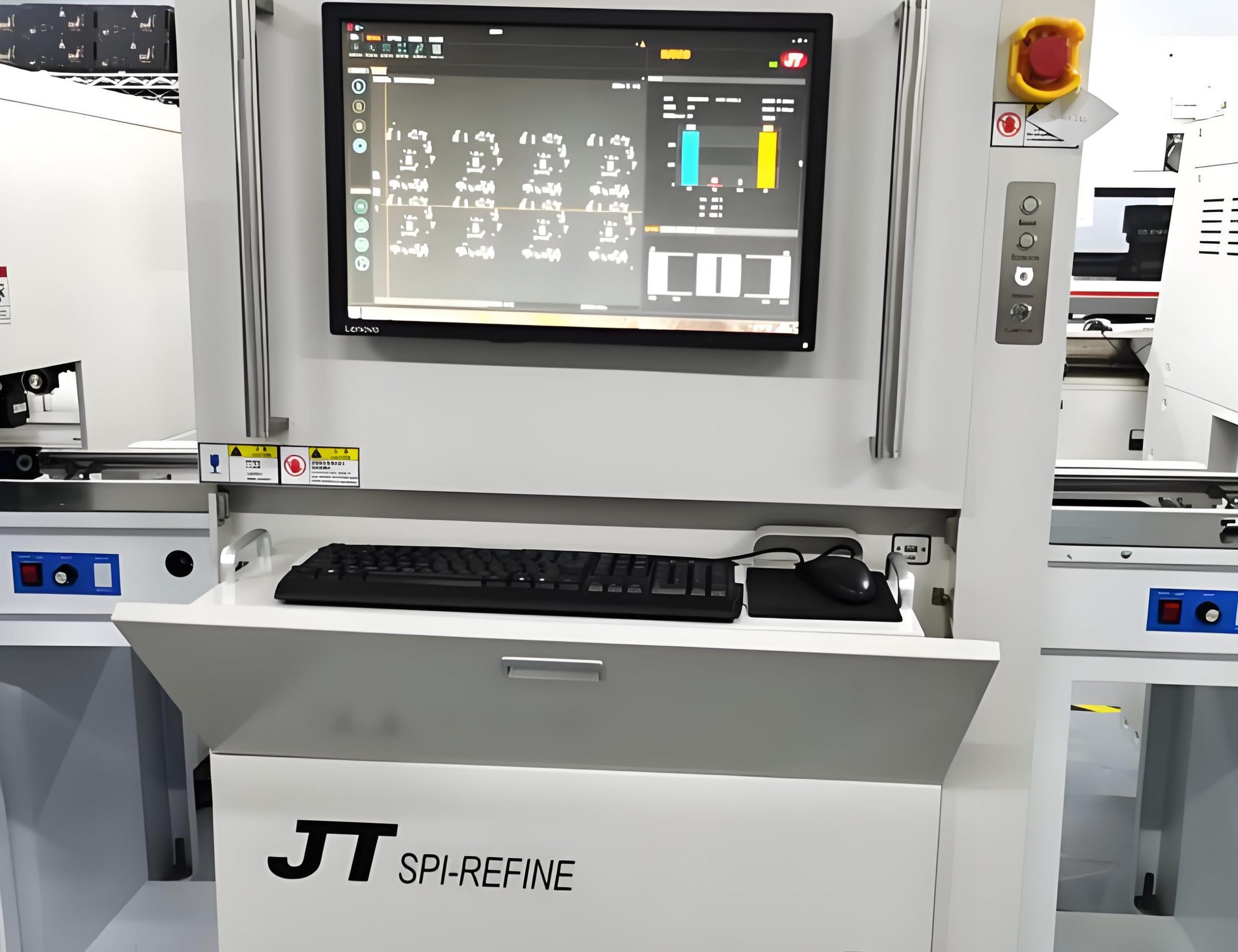
- Pass/Fail Judgment & Reporting: Each deposit is judged as Pass or Fail based on tolerance limits. The board receives an overall verdict. All data, including defect maps and SPC charts, is logged for review and process analysis.
Key Technology Components:
| Component | Function in SPI Process |
|---|---|
| High-Resolution Camera | Captures detailed images for 2D analysis and aids 3D reconstruction. |
| 3D Sensor (Laser/Phase-Shift) | The core component that generates the height data for volumetric measurement. |
| Precision Motion System | Ensures accurate and repeatable scanning of the entire PCB area. |
| Advanced Inspection Software | The “brain” that processes data, applies algorithms, and executes pass/fail decisions. |
In essence, a 3D solder paste inspection system acts as a high-speed, micron-precision 3D scanner for solder paste, providing the actionable data needed for true process control.
What Is the Purpose of Using an Automated Solder Paste Inspection Machine?
The purpose of solder paste inspection extends far beyond simple fault detection. Implementing an automated solder paste inspection machine is a strategic investment aimed at transforming the entire SMT production philosophy from reactive to proactive. Its core purpose is to serve as the primary feedback mechanism for the printing process, enabling a closed-loop control system that ensures consistent, high-quality output.
The fundamental purposes are:
- Prevent Costly Escapes: The primary goal is to catch printing defects beforecostly components are added and the board is reflowed. This prevents the amplification of value-add to defective boards.
- Eliminate Subjective Judgment: It replaces the inconsistency of human visual solder paste printing inspection with objective, repeatable, and quantifiable measurements.
- Generate Process Knowledge: It provides the empirical data needed to understand and control the printing process, answering “how is our process performing?” with numbers, not guesses.
- Enable Continuous Improvement: The wealth of SPC data allows engineers to make informed adjustments to printer parameters, stencil design, and paste management, driving ongoing yield improvements.
- Ensure Standard Compliance: It provides documented, quantitative evidence that the printing process adheres to internal and global solder paste inspection standards like IPC, which is crucial for audits and high-reliability applications.
In short, the purpose of using an automated solder paste inspection machine is to establish a data-driven foundation for quality, turning the solder paste printing process from a potential liability into a documented strength.
Why Manufacturers Choose Advanced SPI Solder Paste Inspection Systems for SMT Production?
Manufacturers choose advanced SPI solder paste inspection systems not as an optional checkpoint, but as a critical production tool for competitiveness and profitability. The decision is driven by tangible returns on investment (ROI) and the need to overcome the limitations of older or manual methods, especially with today’s complex assemblies.
Key drivers for adoption include:
- Dramatic Rework Cost Reduction: By finding defects at the print stage, rework cost can be reduced by up to 90% compared to post-reflow repair. This is the most direct and significant financial benefit.
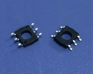
- Essential for Advanced Components: The rise of micro-BGAs, 01005 chips, and QFNs makes 3D solder paste inspection non-negotiable. Human eyes or 2D systems cannot reliably assess the volume of these tiny, hidden deposits.
- Achieving Six Sigma & High Yields: To reach and sustain first-pass yields above 99.5%, proactive process control is mandatory. SPI provides the critical data (Cp/Cpk) needed for Six Sigma manufacturing.
- Closed-Loop Printer Correction: Advanced systems can feed measurement data back to the stencil printer to automatically adjust alignment or pressure, creating a self-correcting “smart” SMT line.
- Supply Chain & Customer Assurance: Providing SPI data to customers demonstrates a commitment to quality and process control, building trust and qualifying for high-reliability contracts in automotive, medical, or aerospace.
Choosing a system from a leader like Koh Young solder paste inspection or similar tier-one providers ensures access to cutting-edge algorithms, robust hardware, and global support, safeguarding the investment.
Key Solder Paste Inspection Criteria Used in Global IPC Standards
Professional solder paste inspection relies on well-defined, industry-accepted criteria to ensure consistency and reliability. The IPC (Association Connecting Electronics Industries) standards provide this global framework. While manufacturers may set tighter internal limits, IPC guidelines form the common baseline. Key solder paste inspection parameters defined by standards like IPC-A-610 (Acceptability of Electronic Assemblies) and IPC-J-STD-001 (Requirements for Soldered Electrical and Electronic Assemblies) include:
The evaluation is based on paste deposit geometry. Here are the primary solder paste inspection criteria:
- Volume: The percentage of paste volume relative to the ideal (stencil aperture volume). IPC typically suggests a process control window (e.g., ±50% of nominal), with tighter limits for critical components.
- Height: The measured paste height. Insufficient height can cause opens; excessive height can lead to bridging or tombstoning.
- Area Coverage: The percentage of the pad covered by the paste. Inadequate coverage can result in weak joints.
- Alignment/Registration: The XY offset of the paste deposit centroid from the center of the pad. Significant misalignment can cause opens or shorts.
- Bridging: Any unintended connection of paste between two or more adjacent pads. This is a direct defect (Fail).
Example of SPI Parameter Limits (General Guidance):
| Inspection Parameter | Typical Process Control Target (IPC-aligned) | Defect (Fail) Threshold |
|---|---|---|
| Paste Volume | 80% – 150% of nominal | < 50% or > 200% |
| Paste Height | ±4 mils (≈±100µm) from nominal | Outside of process window |
| Area Coverage | > 75% | < 50% |
| XY Alignment | < 25% of pad width/misalignment | > 50% of pad width/misalignment |
| Bridging | Zero tolerance | Any detectable bridge |
Adhering to these solder paste inspection limits ensures that the process is capable of producing solder joints that will meet IPC acceptability standards after reflow.
Common Solder Paste Inspection Defects and What Causes Them
Identifying solder paste inspection defects at the SPI stage is the key to preventing downstream solder joint failures. Each defect has a root cause in the printing process. Understanding this link allows for rapid correction.
Here are the most common solder paste inspection defects and their typical causes:
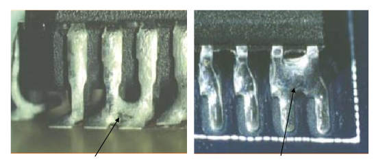
- Insufficient Paste / Low Volume:
- Appearance: The paste deposit is too shallow or small, lacking sufficient volume.
- Primary Causes: Stencil aperture clogging, inadequate printing pressure/speed, low solder paste viscosity, worn or damaged squeegee blade.
- Excessive Paste / High Volume:
- Appearance: The paste deposit is too tall or has excessive volume, risking bridging.
- Primary Causes: Stencil-to-PCB separation (snap-off) too slow, excessive printing pressure, incorrect stencil aperture size, paste slump.
- Misalignment / Registration Error:
- Appearance: The paste deposit is offset from the intended PCB pad.
- Primary Causes: Incorrect PCB fiducial recognition, misalignment between stencil and PCB, board stretch or distortion, printer calibration error.
- Bridging:
- Appearance: Solder paste connects two or more adjacent pads that should be electrically isolated.
- Primary Causes: Excessive paste volume, stencil damage or poor aperture wall quality, incorrect stencil design (insufficient web width), PCB pad contamination.
- Paste Smearing / Peeling:
- Appearance: Paste is smeared outside the pad area or partially peeled away.
- Primary Causes: Wiped or contaminated stencil bottom, incorrect printer cleaning settings, sticky or low-tack solder paste.
By categorizing defects with an SPI machine, process engineers can immediately target the specific area of the printing process—be it stencil maintenance, printer setup, or paste handling—for correction, dramatically reducing troubleshooting time.
How China PCBA Solder Paste Inspection Manufacturers Improve Yield and Accuracy?
Leading China PCBA solder paste inspection manufacturers and assemblers leverage SPI not just as a quality gate, but as the core of a holistic, data-driven manufacturing strategy. For a China PCBA solder paste inspection factory competing globally, maximizing yield and accuracy is paramount to profitability and reputation. This is achieved through a systematic approach.
Strategies for Superior Performance:
- Investment in Advanced 3D SPI Technology: Top-tier manufacturers deploy the latest 3D solder paste inspection systems from leaders like Koh Young, CyberOptics, or Saki. This ensures the capability to inspect the most demanding assemblies with high speed and precision.
- Integration into Smart SMT Lines: SPI is not a standalone island. It is fully integrated into the MES (Manufacturing Execution System), creating a closed-loop where inspection data automatically feeds back to the stencil printer for real-time correction and to the front-end for process optimization.
- Rigorous Process Parameter Management: They establish and meticulously monitor strict solder paste inspection parameters and tolerances, often tighter than IPC standards, to maintain a high process capability index (Cpk > 1.67).
- Data Analytics for Predictive Maintenance: The wealth of SPI data is analyzed to predict stencil wear, squeegee blade life, and paste performance degradation, enabling proactive maintenance before defects occur.
- Skilled Process Engineering Teams: They invest in training process engineers to expertly interpret SPI SPC charts, correlate defects to root causes, and continuously fine-tune the entire printing ecosystem (stencil, printer, paste, environment).
By combining cutting-edge solder paste inspection equipment with deep process expertise and data integration, these manufacturers transform SPI from a cost center into a yield-assurance and continuous-improvement engine.
What Are the Latest Trends in 3D Solder Paste Inspection Technology?
The evolution of 3D solder paste inspection technology is driven by the need for higher speed, greater precision, smarter analytics, and deeper integration. Modern 3D solder paste inspection systems are becoming more intelligent and connected. Key trends shaping the future of SPI include:
- AI-Powered Defect Detection and Classification: Moving beyond simple threshold-based rules, AI and machine learning algorithms are being trained to identify complex and novel defect patterns, improving accuracy and reducing false calls, especially on challenging boards.
- True 3D Measurement for Sides of Deposits: Beyond just volume and height, advanced systems are now capable of analyzing the side-profile shape and slump of paste deposits, providing even deeper insight into print quality.
- Enhanced Speed for High-Mix Production: As product lifecycles shorten, SPI systems are being optimized for faster programming and board changeover, minimizing downtime in high-mix, low-volume (HMLV) environments.
- Seamless Integration with Industry 4.0: SPI is a key data node in the smart factory. The trend is toward seamless data exchange with MES, ERP, and printer systems, enabling full traceability, predictive analytics, and autonomous process optimization.
- Combined Inspection Platforms (SPI + AOI): There is a growing trend towards platforms that combine 3D SPI and 3D Automated Optical Inspection (AOI) either in a single machine or a tightly coupled line, providing a complete pre- and post-reflow quality picture.
These advancements ensure that 3D solder paste inspection remains a vital and evolving technology, capable of meeting the future challenges of miniaturization and smart manufacturing.
Why Choose BEST Technology for Reliable PCBA Production Backed by Expert Solder Paste Inspection?
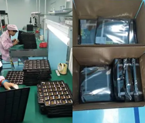
Choosing the right manufacturing partner is essential when your project requires precise solder paste inspection and stable PCBA quality. At BEST Technology, our China and Vietnam factories are equipped with advanced SMT production lines and industry-leading SPI systems, ensuring every build—whether prototype or mass production—meets strict reliability standards.
Advanced SPI Systems for High-Accuracy Printing Control
We utilize professional in-line SPI solutions to monitor solder paste height, volume, area, and alignment in real time, helping prevent early-stage defects and improving first-pass yield.
Strong Manufacturing Capability in China and Vietnam
With PCB fabrication in China and SMT assembly facilities across China and Vietnam, we offer stable capacity, flexible lead times, and optimized production planning for global customers.
Full PCBA Services From Prototyping to Mass Production
Whether you need rapid PCB prototyping, small-batch assembly, or high-volume turnkey production, we provide complete support—including component sourcing, stencil design, and box-build assembly.
Strict Quality Control Following IPC and ISO Standards
Our plants operate under ISO 9001 and IPC Class 2 / Class 3 requirements, ensuring that every solder joint, print deposit, and assembled board follows international quality benchmarks.
Experienced Engineering Team Offering DFM and Technical Support
Our engineers review your Gerber files, BOM, stencil apertures, and printing parameters to help reduce defect rates and optimize manufacturing processes before production even begins.
Proven Export Experience With Global Clients
We serve customers in Europe, the United States, the Middle East, and Asia—especially Germany, Israel, and the USA—ensuring professional communication and reliable shipment handling.
BEST Technology combines advanced solder paste inspection capability with strong PCBA manufacturing capacity to deliver consistent quality and dependable performance. If you need a trusted partner for your next PCB or PCBA project, contact us at sales@bestpcbs.com and our team will respond with a fast, accurate quotation tailored to your requirements.
All in all, solder paste inspection is the indispensable first line of defense in achieving superior PCBA reliability, yield, and overall value. This article has explored its critical function, from the core solder paste inspection process and criteria to the advanced technology and strategic benefits it provides. In a competitive landscape, partnering with a manufacturer that prioritizes and masters this foundational process is key. BEST Technology integrates state-of-the-art solder paste inspection systems and deep process expertise into every project, from standard PCBs to advanced ceramic substrates. Pls feel free to contact our team at sales@bestpcbs.com to discuss your next SMT PCBA project.
FAQs About Solder Paste Inspection
Q1: What solder paste brands and compositions do you commonly use?
We use different solder paste brands for domestic and overseas production:
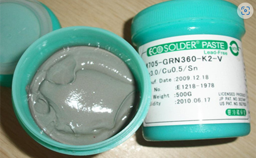
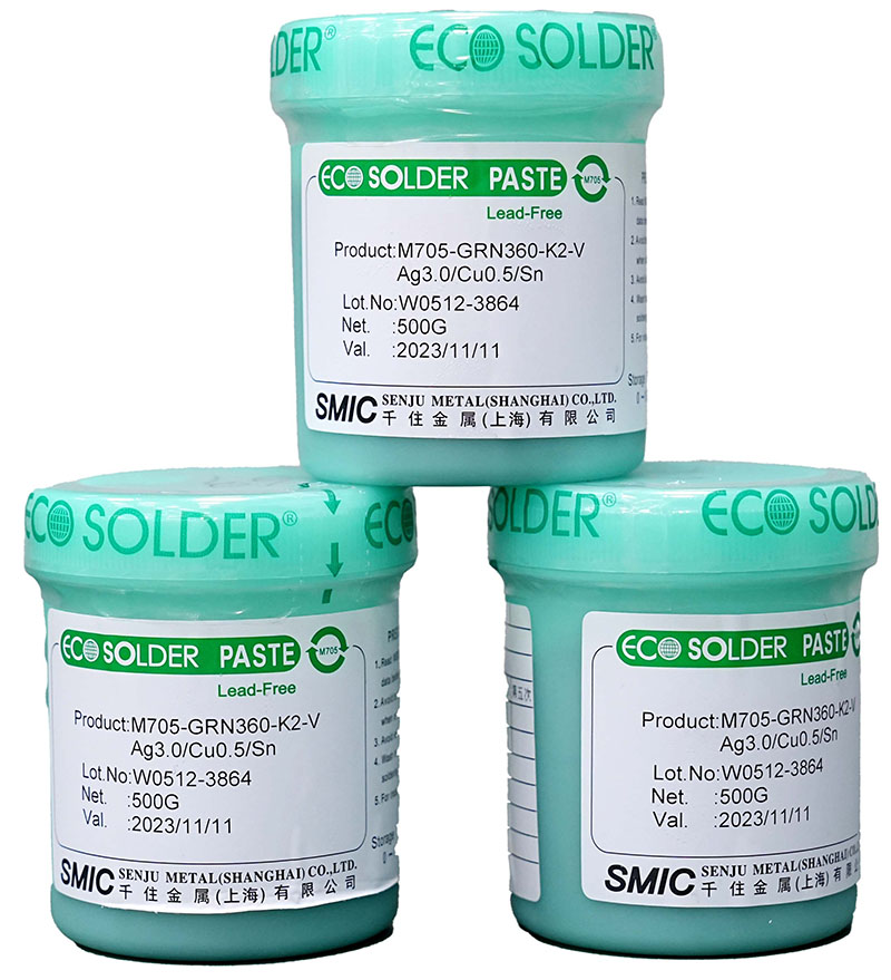
• For overseas projects, we use the Japanese brand Senju with the composition Sn96.5%, Ag3.0%, Cu0.5%.
• For domestic production, we use the Chinese brand Yifenghua with the composition Sn99%, Ag0.3%, Cu0.7%.
Q2: What are the standard solder paste handling conditions?
Our standard handling specifications are:
• Rewarming time: 4 hours
• Stirring time: 3 minutes
• Refrigerated storage temperature: 2–10°C
Q3: What types of stencils do you use in SMT printing?
We mainly use two categories of stencils:
• Standard stencils
• Step stencils (for uneven solder paste height requirements)
Q4: What are the common stencil frame sizes you support?
Typical stencil frame sizes include:
• 37 × 47 cm
• 42 × 52 cm
• 55 × 65 cm
• 73.6 × 73.6 cm
Q5: What stencil thickness options are available?
Our commonly used stencil thicknesses are:
0.06 mm, 0.08 mm, 0.1 mm, 0.12 mm, 0.15 mm, and 0.2 mm