pcb
Home > Blog

Posts Tagged ‘PCB’

Bus Bar Thick Copper Solution, Solderable PCB Bus Bars
星期一, 24 2 月, 2025

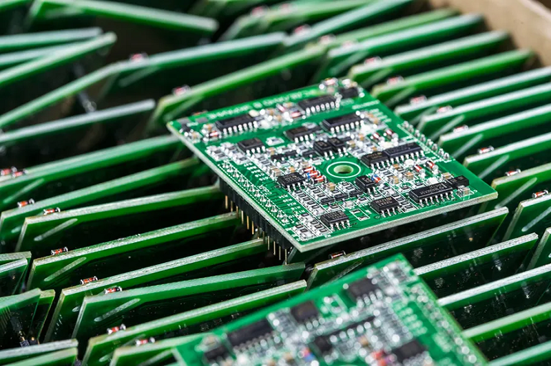
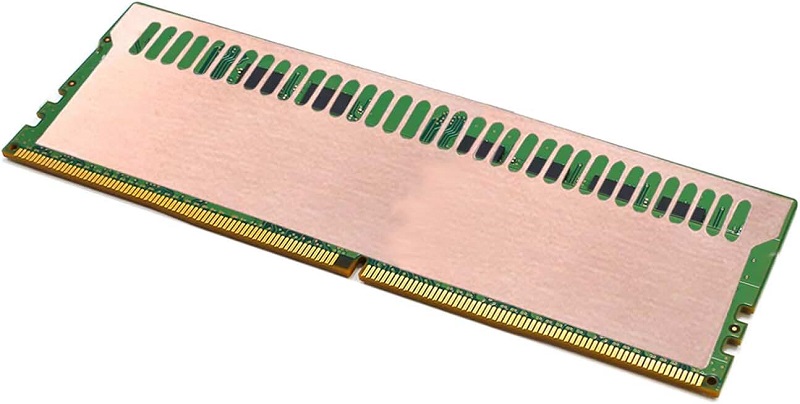
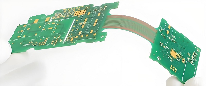
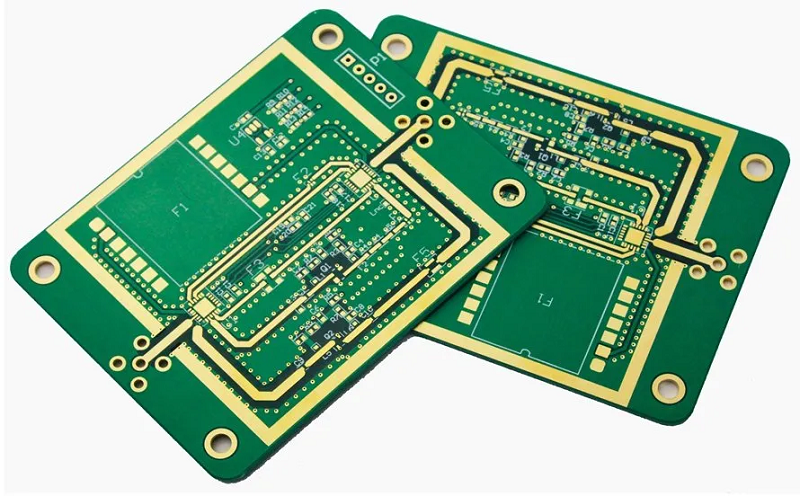
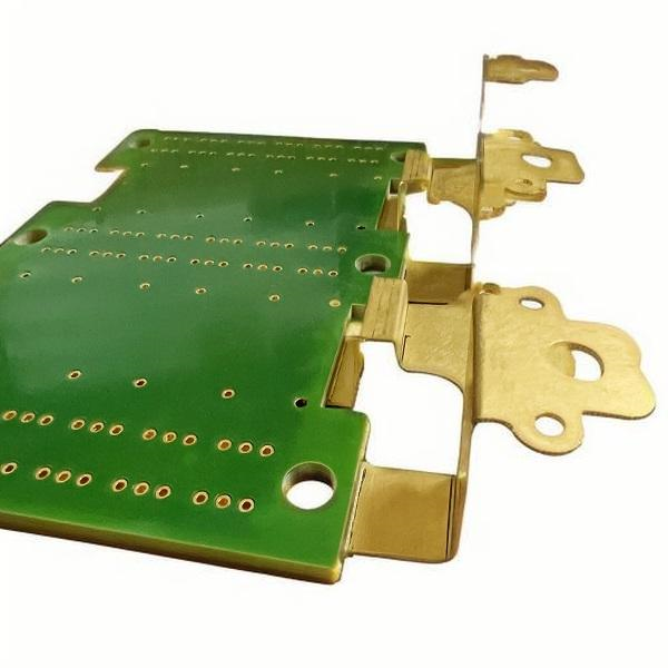
Bus bar thick copper solution is essential for handling high currents in PCB designs. Standard copper traces often struggle with power distribution, leading to heat buildup and inefficiencies. This is where solderable PCB bus bars come in—they offer lower resistance, better heat dissipation, and improved mechanical strength compared to standard traces. Best Technology is a trusted leader in providing advanced bus bar thick copper solutions, with over 18 years of experience in producing high-quality PCBs for diverse applications.

But what exactly is a busbar PCB? How does thickness affect performance? What materials and coatings are best? This article answers these questions and more, helping you choose the right solution for your application.

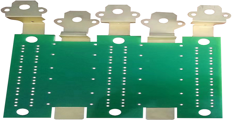
What is a Busbar PCB?

A busbar PCB is a circuit board that includes a thick copper busbar to distribute current efficiently. Unlike standard copper traces, a busbar provides a solid and stable electrical connection, making it perfect for power electronics, inverters, and high-current applications.

In traditional PCBs, thin copper layers handle electrical signals, but high-current circuits demand thicker conductors to prevent overheating. This is why pcb busbars are used—they significantly reduce resistance, improve power handling, and enhance overall reliability.

Additionally, different types of busbars exist based on mounting style, such as:

PCB stiffener busbars – Add structural strength to the board.

PCB mount bus bars – Designed for easy attachment to circuit boards.

SMD bus bars – Surface-mount busbars for compact electronic designs.

SMT bus bars – Ideal for automated assembly processes.

Each type offers unique benefits depending on the application.

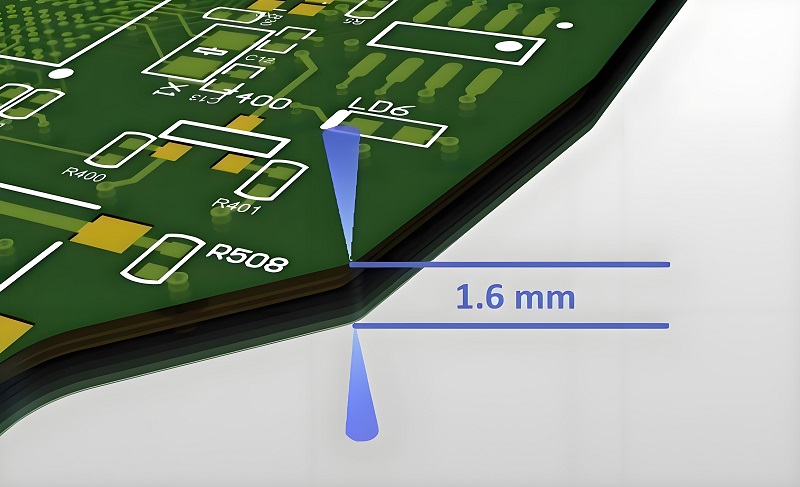
What is the Thickness of Copper Busbars?

The thickness of a copper busbar depends on the current load and heat dissipation requirements. Common thicknesses range from:

0.5 mm to 1 mm for low-power applications.

1 mm to 3 mm for medium-current circuits.

3 mm to 5 mm or more for high-current industrial applications.

A thicker pcb busbar means lower electrical resistance and better thermal performance, ensuring that the PCB operates efficiently without overheating.

What Copper Material is Used in Bus Bars?

Copper busbars need to be highly conductive and durable. The two most commonly used copper types are:

Electrolytic Tough Pitch (ETP) Copper (C11000) – The most widely used type, with 99.9% pure copper content, offering high electrical and thermal conductivity.

Oxygen-Free High-Conductivity (OFHC) Copper (C10200) – Contains even fewer impurities, making it more resistant to oxidation and ideal for high-performance applications.

Both materials are excellent for pcb mount bus bars, but OFHC copper is preferred when superior conductivity and durability are required.

What Grade of Copper is Used in Busbars?

Copper busbars typically use C11000 or C10200 copper, both of which are high-purity grades. C11000 is more cost-effective, while C10200 offers better oxidation resistance and is used in demanding environments.

For solderable pcb bus bars, copper should have a smooth surface and be compatible with tin or silver coatings for improved solderability.

What is the Coating on Copper Bus Bars?

Copper busbars are coated to prevent oxidation and enhance conductivity. Common coatings include:

Tin – The most common coating, offering corrosion resistance and easy soldering.

Silver – Improves conductivity and is often used in high-frequency applications.

Nickel – Increases durability and is used in harsh environments.

Among these, solderable busbars often feature tin coating, which balances protection, conductivity, and ease of assembly.

How Thick is the Tin Coating on a Busbar?

Tin coatings on busbars typically range from 1 to 10 microns.

1-3 microns – Suitable for standard applications.

5-10 microns – Used in harsh environments for added protection.

A properly coated solderable busbar prevents oxidation while maintaining good solder adhesion.

How to Join a Copper Busbar?

There are several methods to join copper busbars in PCBs:

Soldering – The most common method for solderable pcb bus bars, ensuring a strong electrical connection.

Brazing – Uses a filler metal to bond busbars at higher temperatures, creating a stronger joint.

Bolting – Allows for easy disassembly and maintenance but may increase contact resistance.

Welding – Used for permanent, high-strength connections, ideal for high-power circuits.

Choosing the right method depends on electrical, mechanical, and thermal considerations.

Why is a Busbar Not Insulated?

Many copper busbars are left uninsulated to improve heat dissipation. Since busbars handle high currents, insulation could trap heat, affecting performance.

However, some applications require insulation to prevent short circuits. In such cases, materials like PVC, epoxy, or heat-shrink tubing are applied.

Can You Bend Copper Busbars?

Yes, copper busbars can be bent to fit PCB layouts. However, bending must be done carefully to prevent:

Cracks – Too much force can damage the copper.

Stress points – Overbending weakens conductivity.

Incorrect alignment – Poor bending can affect PCB assembly.

The key is using a proper bending radius to maintain mechanical strength and conductivity.

What Are the Advantages of Using Copper Bus Bars in PCBs?

Copper busbars provide several benefits in PCBs, including:

Lower electrical resistance – Reduces energy loss.

Better heat dissipation – Keeps components cool.

Stronger mechanical structure – Increases durability.

Compact design – Simplifies PCB layout.

For high-power applications, a bus bar thick copper solution is essential for efficient and reliable performance.

How Do Solderable PCB Busbars Differ from Other Types?

Unlike press-fit or bolt-on busbars, solderable busbars are designed for direct PCB mounting. They have a tin coating for better solderability, making them ideal for surface-mount applications (SMD bus bar, SMT bus bar), compact, high-current PCB designs, and automated assembly processes. They ensure a stable electrical connection, reducing contact resistance and improving longevity.

    To sum up, a A bus bar thick copper solution enhances PCB reliability and efficiency. Selecting the right bus bar thick copper solution is crucial for high-power PCB designs. Whether using solderable pcb bus bars, pcb mount bus bars, or smd bus bars, choosing the right thickness, material, and coating ensures better efficiency and durability.

    For businesses seeking high-performance busbars, working with an experienced manufacturer ensures the best results. With the right choice, power electronics, renewable energy systems, and industrial applications can achieve better performance, lower energy loss, and improved reliability. If you’re looking for high-quality PCB busbars, get in touch with Best Technology at sales@bestpcbs.com to explore the best bus bar thick copper solutions for your need. Our focus on innovation and customer satisfaction ensures we deliver reliable, efficient, and cost-effective copper bus bar solutions tailored to meet the unique needs of the electronics industry.

    Microprocessor PCB: What is PCB in Microprocessor?
    星期五, 21 2 月, 2025

    A microprocessor PCB is a vital part of many modern electronic devices. But what exactly does it mean, and how does it function in a microprocessor? Understanding the role of a microprocessor PCB can help you appreciate its importance in everything from smartphones to industrial equipment. In this artical, we will explore the design, programming, components, and applications of microprocessor PCBs, giving you a comprehensive look into this essential technology.

    What Is a Microprocessor PCB?

    A microprocessor PCB is a type of printed circuit board (PCB) specifically designed to house a microprocessor, which is the brain of electronic systems. It connects various components like memory, input/output devices, and power supplies, enabling the microprocessor to perform its tasks efficiently. The PCB serves as a platform for mounting the microprocessor and other necessary components while providing the electrical connections between them.

    Microprocessor PCBs are often designed to be compact and efficient, ensuring that the microprocessor can execute complex calculations and commands with minimal power consumption. In addition, these boards are typically built to withstand heat and electrical interference, which are crucial in maintaining long-term functionality.

    Is a Microprocessor a Circuit Board?

    A microprocessor itself is not a circuit board. It is an integrated circuit (IC) that contains the core processing unit of a device. However, a microprocessor PCB provides the physical structure and electrical pathways needed to connect the microprocessor with other components of the system. In essence, the PCB acts as a support system for the microprocessor, allowing it to interact with memory, sensors, and other devices necessary for the functioning of electronic systems.

    The relationship between the microprocessor and its PCB is similar to that of a brain and a nervous system, where the brain (microprocessor) performs tasks and the nervous system (PCB) carries the signals to and from various parts of the body (electronic components).

    What Are the Key Components in Microprocessor PCBs?

    When looking at microprocessor PCBs, several critical components work together to ensure the system performs efficiently:

    Microprocessor: The heart of the PCB, responsible for executing instructions and processing data.

    Capacitors: These help stabilize voltage levels and filter out noise, ensuring that the microprocessor gets a steady supply of power.

    Resistors: Used to control the flow of electrical current, protecting sensitive components and ensuring proper functionality.

    Inductors: Help in power supply management, especially in circuits requiring smooth current flow.

    Connectors: Allow communication between the PCB and external devices, such as displays, storage devices, or sensors.

    These components work in harmony to ensure the microprocessor functions smoothly within the PCB, providing reliable performance for the device it powers.

    What Is the Difference Between a CPU and a PCB?

    A CPU (Central Processing Unit) is the primary component responsible for processing instructions in a computer or other electronic device. It executes the tasks needed by the system, including calculations, logic operations, and data management. On the other hand, a PCB (Printed Circuit Board) is a physical platform that supports the CPU and other components. The PCB provides the necessary connections between the CPU, memory, and other elements, enabling them to work together seamlessly.

    While the CPU is responsible for processing data, the PCB serves as the foundation that connects all parts of the system. In short, the CPU is the “brain,” and the PCB is the “nervous system.”

    How Do Microprocessor PCBs Work in Devices?

    A microprocessor PCB functions by providing a stable environment for the microprocessor to operate. It enables communication between the microprocessor and other essential components like memory, power supplies, and input/output devices. The PCB also acts as a physical connector that links these components, allowing data to flow between them.

    For instance, in a smartphone, the microprocessor on the PCB controls various tasks, from processing inputs from the touchscreen to managing the device’s power consumption. The PCB connects all the necessary components—like the display, memory, and wireless modules—to the microprocessor, allowing the device to perform its functions smoothly.

    How Is a Microprocessor PCB Programmed?

    Microprocessor PCB programming involves writing software that allows the microprocessor to perform specific tasks. The programming is done through firmware, which is embedded into the microprocessor’s memory. Firmware is a set of instructions that tells the microprocessor how to process data and communicate with other parts of the system.

    Programming a microprocessor PCB typically requires knowledge of low-level programming languages like C or assembly. Engineers write the code, which is then uploaded to the microprocessor through a programmer device. Once the firmware is loaded, the microprocessor begins performing its tasks, interacting with the other components on the PCB to control the system’s operations.

    What Challenges Come with Designing Microprocessor PCBs?

    Designing microprocessor PCBs can be a complex task due to several challenges that must be addressed:

    Signal Integrity: Ensuring that signals remain clear and stable is critical, as any interference can disrupt the microprocessor’s operation.

    Heat Management: Microprocessors generate heat, which can affect performance. Proper heat dissipation methods, such as heatsinks or thermal vias, are essential.

    Power Distribution: Ensuring the microprocessor receives a stable power supply without noise or fluctuations is crucial for smooth operation.

    Size Constraints: As devices get smaller, the PCB must be compact enough to fit into tight spaces without compromising performance.

    Despite these challenges, skilled engineers can design microprocessor PCBs that perform efficiently and reliably.

    Where Are Microprocessor PCBs Used in Electronics?

    Microprocessor PCBs are used in a wide range of electronic devices, from everyday gadgets to industrial machinery. Some common applications include:

    Smartphones: Microprocessor PCBs control everything from touch input to wireless communication.

    Computers: In desktops and laptops, microprocessor PCBs manage data processing, memory, and input/output functions.

    Automobiles: Modern vehicles rely on microprocessor PCBs for engine control units, infotainment systems, and safety features like airbags.

    Home Appliances: Devices like microwaves, washing machines, and refrigerators use microprocessor PCBs to control their functions.

    These examples show how integral microprocessor PCBs are to a wide array of industries and technologies.

    A microprocessor PCB is a critical component that ensures the smooth functioning of many modern electronic devices. From providing a stable platform for the microprocessor to connecting essential components and ensuring communication, the PCB is the backbone of electronics. Whether it’s a smartphone, computer, or industrial machine, microprocessor PCBs are essential to the devices we use every day. Understanding how they work, how they are programmed, and the challenges involved in designing them can help you make informed decisions when selecting a supplier for your PCB needs. As a leading ODM and OEM PCB manufacturer, Best Technology offers high-quality microprocessor PCBs tailored to meet your specific requirements, ensuring top-notch performance and reliability. Get in touch with us at sales@bestpcbs.com for any questions or additional information.

    PCB Board: What Does a PCB Stand For?
    星期五, 21 2 月, 2025

    PCB board stands for Printed Circuit Board, a vital component used in nearly all electronic devices. It serves as the backbone for connecting various electronic components, such as resistors, capacitors, and microchips, to ensure they work together efficiently. The PCB acts as a physical support and an electrical connection for these components. Understanding how a PCB board functions, its design process, and its costs can help manufacturers and engineers when creating new devices or products.

    In this article, we will dive into the essential aspects of PCB boards, from their design and creation to maintenance and testing. We’ll also explore their various types, materials, and how much they cost, helping you make informed decisions whether you’re designing your own circuit board or sourcing from PCB board manufacturers.

    What Does a PCB Stand For?

    PCB stands for Printed Circuit Board. It is a flat, non-conductive material that supports and connects electronic components via conductive pathways etched or printed onto the board. These pathways, often made of copper, form the electrical circuits that allow devices to function. PCBs come in various shapes and sizes, depending on the complexity and requirements of the devices they support. They’re found in everything from smartphones to household appliances and even in large industrial machines. Understanding the definition and the purpose of a PCB board is essential before diving into its design and creation process.

    How to Design a PCB Board?

    Designing a PCB board begins with understanding the circuit requirements. The design process typically involves several stages:

    Schematic Design: This is the initial stage where the electrical components are selected, and the circuit is drawn.

    PCB Layout: In this stage, the physical layout of the components on the board is planned, considering space, component size, and heat dissipation.

    Routing: The routing phase involves laying down copper traces to connect components.

    Verification: A thorough review and testing phase to ensure that the design works as intended.

    For a successful PCB board design, it is essential to use specialized software tools like Eagle, Altium Designer, or KiCad. These programs allow for detailed and precise layout planning.

    How to Make a PCB Board?

    Making a PCB board requires several steps, which involve both manual and machine processes. Here’s a basic overview:

    Create the PCB Design: First, design the PCB using software.

    Print the Design: Once the design is ready, print it onto a copper-coated board.

    Etch the Board: Use chemicals to remove unwanted copper, leaving behind the circuit design.

    Drill Holes: If necessary, drill holes for components like resistors and capacitors.

    Apply Soldermask and Silkscreen: These layers protect the copper traces and display component information, respectively.

    Solder Components: Finally, solder the components into place.

    This process can be done in-house with the right equipment or outsourced to professional printed circuit board manufacturers.

    How to Clean a PCB Board?

    Cleaning a PCB board is important to ensure it remains free of dust, oils, and other contaminants that could impact its performance. To clean your PCB:

    Use Isopropyl Alcohol: Apply a small amount of isopropyl alcohol (preferably 99%) to a soft brush or cloth.

    Gently Scrub the Board: Lightly scrub the surface to remove dirt or residue.

    Dry the Board: After cleaning, let the board dry completely before use.

    Always avoid using abrasive materials that could damage the surface of the PCB.

    How to Solder Wire to PCB Board?

    Soldering wires to a PCB board requires precision. Here’s how to do it:

    Prepare the Tools: You’ll need a soldering iron, solder, flux, and wire.

    Apply Flux: Lightly apply flux to the pads where the wire will be soldered.

    Heat the Soldering Iron: Heat the soldering iron to around 350°C.

    Solder the Wire: Place the wire on the pad and apply the solder to the joint. Remove the soldering iron and let the joint cool.

    Proper soldering ensures a solid, reliable connection.

    How to Cut a PCB Board?

    Cutting a PCB board is a simple task but requires care to avoid damaging the board. Here’s how to do it:

    Mark the Cutting Line: Use a pencil or marker to draw a straight line where you want to cut.

    Use a PCB Cutter or Dremel: A specialized PCB cutter or Dremel tool with a cutting disk is ideal for clean, straight cuts.

    Smooth the Edges: After cutting, use a file to smooth any rough edges.

    Cutting the PCB allows it to fit into specific devices or designs. Always wear protective gear while cutting.

    How to Test a PCB Board?

    Testing a PCB board involves checking its electrical functionality. You can use several methods:

    Visual Inspection: Look for any obvious issues, such as broken traces, soldering issues, or misplaced components.

    Functional Testing: Power the circuit and verify if the board operates as expected.

    Automated Testing Equipment (ATE): High-tech equipment can test multiple points on the PCB simultaneously.

    Testing ensures the PCB performs correctly and meets quality standards.

    How to Read a PCB Board?

    Reading a PCB board involves interpreting the layout and understanding the component functions. You should:

    Identify Components: Look for the labels next to the components, which should indicate their type (e.g., R for resistors, C for capacitors).

    Understand the Traces: Follow the copper traces to understand how power and signals flow between components.

    Check for Connections: Ensure that the components are properly connected, with no short circuits or unconnected pads.

    Reading a PCB board is crucial when troubleshooting or making modifications.

    How to Check a PCB Board with Multimeter?

    A multimeter is a valuable tool for checking a PCB board. Here’s how you can use it:

    Set the Multimeter to Continuity Mode: This will allow you to test whether there are any open circuits.

    Check the Connections: Place the multimeter probes on two points that should be connected, and verify continuity.

    Measure Resistance: Check for components that should have specific resistance values to ensure they are working correctly.

    Regular checks with a multimeter can help ensure the PCB board’s functionality and durability.

    How Much Does a PCB Board Cost?

    The cost of a PCB board varies. Simple prototypes start around $5–$50 each. Bulk orders drop prices to $0.10–$10 per board. Key factors

    Size/Layers: Bigger or multi-layer boards cost more

    Material: Standard FR-4 is cheaper; special materials (flexible, high-frequency) add cost.

    Quantity: Higher volume = lower per-unit price.

    Turnaround: Faster delivery increases cost.

    Looking for an accurate quote? Share your specifications on our website for fast and competitive pricing!

    In conclusion, PCB boards are the foundation of modern electronics, connecting components and ensuring devices function smoothly. Understanding their design, manufacturing, and maintenance is crucial for anyone working with electronics. Whether you’re designing a PCB board, testing its functionality, or sourcing from printed circuit board manufacturers, having the right knowledge can make all the difference.

    Best Technology has over 18 years of experience in the PCB industry, providing top-quality PCBs for a variety of applications. We offer a range of materials and services to meet your specific needs, ensuring you receive reliable and cost-effective solutions. For details or inquiries, feel free to contact us at sales@bestpcbs.com.

    Bulk Conductivity of Copper: What Is The Bulk Conductivity?
    星期四, 20 2 月, 2025

    Bulk conductivity of copper is a fundamental property that defines how well the material can conduct electricity. This feature makes copper a leading material in a variety of electrical applications, including printed circuit boards (PCBs). Whether in power transmission or complex electronics, understanding how bulk conductivity influences performance is essential for selecting the right materials. In this blog, we’ll explore the significance of copper’s electrical properties, its comparison to other materials, and how these properties affect the design and performance of PCBs.

    What is the Bulk Conductivity?

    Bulk conductivity refers to the ability of a material to conduct electric current throughout its entire volume. This property is influenced by factors such as the material’s atomic structure and the presence of impurities. In simple terms, it measures how easily electrical charges can flow through the material when an electric field is applied. Copper, with its excellent bulk conductivity, is a top choice for electrical wiring and PCBs because of its efficiency in transmitting electrical signals.

    What is the Conductivity of Copper?

    Copper stands out due to its high electrical conductivity. The electrical conductivity of copper is about 5.8 × 10⁷ S/m, which is one of the highest of any metal. This makes it an ideal material for electrical wiring, connectors, and components in PCBs. Its high conductivity ensures that electrical signals travel with minimal resistance, enhancing the efficiency of devices.

    This conductivity is essential when it comes to maintaining high-speed data transmission and power distribution. Copper’s low resistance reduces energy loss, ensuring devices run efficiently, which is why it’s so widely used in the electronics industry.

    What is the Bulk Resistivity of Copper?

    Bulk resistivity is essentially the inverse of conductivity and indicates how much a material resists the flow of electric current. Copper’s resistivity is very low—around 1.68 × 10⁻⁸ Ω·m, making it an excellent conductor. This low resistivity contributes to copper’s superior performance in applications that demand high-efficiency electricity flow, such as in the production of PCBs, which rely on copper’s excellent electrical properties.

    In terms of practical applications, low resistivity allows copper to handle higher currents without excessive heat buildup, a critical factor in maintaining the reliability and longevity of electrical systems.

    What is the High Electrical Conductivity of Copper?

    The high electrical conductivity of copper is a key reason it’s used in almost all electrical wiring and devices. The structure of copper atoms allows for easy movement of free electrons, enabling efficient electrical current flow. This characteristic makes copper indispensable in applications where high efficiency and low loss are essential, such as in communication systems, automotive electronics, and renewable energy technology.

    Furthermore, the high conductivity of copper ensures that devices and systems can operate at optimal efficiency without overheating. This makes it a preferred material for high-performance applications.

    What is the Difference Between Conductivity and Resistivity?

    While conductivity and resistivity are closely related, they describe two opposite properties. Conductivity measures a material’s ability to carry an electric current, while resistivity measures how strongly the material resists the flow of that current. The two are mathematically connected: high conductivity means low resistivity, and vice versa.

    Understanding this difference is essential when designing electrical systems. For example, when choosing materials for PCBs, low resistivity (high conductivity) is vital for reducing energy loss and heat production, which ensures the system runs more efficiently and lasts longer.

    What is the Role of Bulk Conductivity in Electrical Circuits?

    The bulk conductivity of copper plays a crucial role in electrical circuits. In any circuit, especially complex ones like those found in PCBs, the conductivity of the materials used determines how easily electrical signals can travel from one point to another. Copper’s high bulk conductivity ensures that signals are transmitted quickly and with minimal interference.

    Moreover, the efficiency of electrical systems is directly linked to conductivity. Poor conductivity materials result in energy loss and potential system overheating, which can reduce the lifespan of electronic devices. Copper’s role in maintaining high conductivity ensures that electronic devices perform at their best for longer periods.

    How Does Copper’s Bulk Conductivity Affect Its Use in PCBs?

    Copper’s bulk conductivity is particularly important in PCBs, as it ensures fast and efficient signal transmission. In PCBs, copper is used to create the traces that connect various components. These traces must have low resistance to avoid energy loss and signal degradation. The high conductivity of copper allows for thinner traces, which in turn makes PCBs more compact and cost-effective.

    Additionally, copper’s excellent conductivity helps reduce the heat generated in PCBs, which is critical for preventing damage to sensitive components. This is especially crucial in high-performance electronics like processors and communication devices.

    What Are the Key Factors Influencing the Bulk Conductivity of Copper?

    Several factors influence the bulk conductivity of copper. Temperature is one of the most significant. As the temperature increases, the atoms in the copper vibrate more, which can hinder the movement of electrons and decrease conductivity. However, the electrical conductivity of copper increases with increase in temperature to a point. Beyond a certain threshold, the increase in resistance becomes more noticeable.

    Another factor is the purity of the copper. Impurities in the copper can introduce obstacles to electron flow, reducing conductivity. High-purity copper, with minimal impurities, offers the best conductivity.

    What Industries Benefit the Most from Copper’s High Bulk Conductivity?

    Industries that rely on high-efficiency electrical systems benefit the most from copper’s high bulk conductivity. This includes the electronics industry, where copper is used in everything from circuit boards to microprocessors. The telecommunications sector also relies on copper for high-speed data transmission lines. Additionally, the automotive industry, particularly in electric vehicles, uses copper in wiring and batteries due to its excellent conductivity.

    Moreover, industries involved in renewable energy, such as solar and wind power, use copper extensively. Copper’s high conductivity ensures that electrical systems in renewable energy applications are both efficient and durable.

    In summary, the bulk conductivity of copper is a key factor in its widespread use across various industries. Its ability to efficiently conduct electricity makes it indispensable in electronics, telecommunications, automotive, and renewable energy sectors. Understanding the role of copper’s conductivity, and how it compares to other materials, can help businesses and engineers make informed decisions when designing electrical systems and devices. With its low resistivity and high conductivity, copper remains the material of choice for a wide range of applications, from power transmission to high-performance PCBs. At Best Technology, we specialize in high-quality, tailor-made PCBs, offering rapid delivery and unmatched customer support. Reach out to us at sales@bestpcbs.com for more information or questions.

    Copper vs Aluminum Thermal Conductivity: Which transfers heat better?
    星期四, 20 2 月, 2025

    Copper thermal conductivity plays a significant role in its widespread use across various industries. When it comes to heat transfer, copper is often seen as the go-to material due to its exceptional ability to conduct heat. In this blog, we will explore how copper compares to other metals, especially aluminum, and how its thermal properties impact its performance in different environments. Let’s dive into the world of heat conductivity, from copper’s efficiency to its temperature-dependent behavior.

    What Is the Thermal Conductivity of Copper?

    Thermal conductivity refers to a material’s ability to conduct heat. Copper stands out as one of the best conductors of heat, making it a popular choice in industries where efficient heat transfer is crucial. The thermal conductivity of copper is approximately 398 W/m·K at room temperature. This high value makes copper the preferred material for various applications, from electrical wiring to heat exchangers.

    Interestingly, pure copper offers even higher thermal conductivity compared to alloys, making it an essential material in applications requiring optimal heat management.

    What Is the Best Conductor of Heat?

    While many metals offer good thermal conductivity, copper is often regarded as the best conductor of heat. Silver, in fact, has a slightly higher thermal conductivity than copper, but due to its cost and scarcity, silver is rarely used in practical applications. Copper’s balance of affordability and efficiency makes it the top choice for industries where heat transfer is critical, such as electronics, automotive, and HVAC systems.

    Aluminum, although a good conductor, falls behind copper in terms of efficiency. Copper’s superior performance in both heat conductivity and durability makes it a more reliable material in most heat management scenarios.

    What Is the Thermal Conductivity of Copper vs Aluminum?

    When comparing the thermal conductivity of copper vs aluminum, copper wins hands down. Aluminum has a thermal conductivity of around 235 W/m·K, which is significantly lower than copper’s. This difference may seem small, but it has a big impact in fields such as electronics and engineering, where heat dissipation is critical.

    Copper’s higher conductivity means that it can transfer heat more effectively, making it a better choice for applications that require rapid heat transfer. However, aluminum’s lighter weight and lower cost make it a viable alternative in situations where heat conductivity is not the top priority.

    How Does Copper Compare to Other Metals in Thermal Conductivity?

    Copper is often compared to metals like aluminum, brass, and nickel. While aluminum is a good conductor, copper far surpasses it in efficiency. On the other hand, brass, which is an alloy of copper and zinc, has lower thermal conductivity than pure copper. Similarly, nickel’s thermal conductivity is also lower than copper’s, which makes copper a preferred material when high heat transfer is needed.

    For instance, silver may have the highest thermal conductivity of all metals, but its cost makes it impractical for most applications. Copper strikes a perfect balance, offering excellent heat transfer without the high price tag associated with silver.

    How Does Temperature Affect Copper’s Thermal Conductivity?

    Copper’s thermal conductivity does not remain constant as temperatures change. As the temperature increases, copper’s thermal conductivity decreases. This is because the atomic vibrations in copper increase with temperature, disrupting the smooth flow of heat.

    At room temperature, copper’s conductivity is at its peak. However, as the temperature rises, its ability to conduct heat diminishes. This temperature-dependent behavior must be considered in high-heat applications such as electronics and manufacturing, where managing temperature fluctuations is critical.

    At What Temperature Does Copper Melt?

    Copper melts at a temperature of 1,984°F (1,085°C). This relatively high melting point is another reason copper is highly favored in industries dealing with extreme temperatures, such as aerospace and power generation. Unlike materials with lower melting points, copper maintains its integrity under heat, providing reliability and durability.

    Is Copper or Aluminum Better for Cooling?

    When it comes to cooling efficiency, copper generally outperforms aluminum due to its superior thermal conductivity. However, aluminum is often used in cooling applications where weight is a crucial factor, such as in the automotive industry. Copper’s heavier weight might make it less suitable for such purposes, but in situations where heat needs to be transferred quickly and efficiently, copper is the better choice.

    In cases like computer processors, where efficient cooling is paramount, copper is often used for heat sinks because of its superior ability to absorb and dissipate heat.

    Why Does Copper Have a High Thermal Conductivity?

    Copper’s high thermal conductivity can be attributed to its atomic structure. The metal has a highly ordered arrangement of atoms, which allows heat to flow more easily through the material. Additionally, copper’s free electrons move quickly, aiding in the rapid transfer of heat. This ability to efficiently conduct heat is one of the reasons copper is so widely used in heat exchangers, electrical wiring, and other applications where heat dissipation is essential.

    In summary, the thermal conductivity of copper makes it the material of choice for a variety of high-performance applications. Whether you’re considering copper vs aluminum thermal conductivity for your projects or exploring how copper compares to other metals like brass or nickel, copper consistently outperforms its competitors in heat transfer efficiency. While aluminum may be lighter and more cost-effective in some situations, copper’s superior thermal properties make it the go-to material in industries where heat management is critical.

    At Best Technology, we specialize in high-quality PCBs designed for optimal thermal performance. With over 18 years of experience in the industry, we provide solutions tailored to your specific needs. If you’re looking for a reliable partner in heat management, reach out to us at sales@bestpcbs.com for more information or questions.

    Thermal Conductivity of Copper: What is the K Value of Copper?
    星期三, 19 2 月, 2025

    Thermal conductivity of copper is one of the most important properties of the material, especially in industries like electronics and heat management. With its high thermal conductivity, copper plays a vital role in efficiently transferring heat, making it a go-to material for various applications, including Printed Circuit Boards (PCBs), heat sinks, and cooling systems. But what exactly is the K value of copper, and why should you care? Let’s dive into the fascinating world of copper’s thermal conductivity and how it impacts the way we use this versatile metal.

    What is the Thermal Conductivity of Copper?

    The thermal conductivity of copper is the measure of how well copper conducts heat. In simpler terms, it defines how easily heat flows through the material. The K value, or thermal conductivity, of copper is exceptionally high, approximately ranging from 380 to 401 W/(m·K), making it one of the most efficient materials for heat transfer. This characteristic is crucial in applications where efficient heat dissipation is required.

    The high thermal conductivity of copper means it can quickly absorb and release heat, which is why it’s widely used in applications such as wiring, heat exchangers, and cooling systems. This ability to efficiently manage heat is especially important in electronics and the manufacturing of PCBs.

    What Factors Affect the Thermal Conductivity of Copper?

    Several factors can influence the thermal conductivity of copper, and understanding them helps optimize copper’s use in various industries.

    Temperature: As temperature increases, copper’s thermal conductivity decreases slightly. However, copper still remains highly conductive compared to most other materials, even at higher temperatures. The temperature dependence of copper’s thermal conductivity is relatively low compared to some other materials.  

    Purity: Pure copper has the highest thermal conductivity. The thermal conductivity of pure copper is approximately 401 W/(m·K). Impurities or alloying elements in copper can reduce its ability to conduct heat. That’s why many applications rely on high-purity copper to ensure optimal thermal performance.

    Structure: The microstructure of copper also plays a significant role. For instance, copper that is in a crystalline form tends to have better thermal conductivity compared to non-crystalline forms.

    External Conditions: Environmental factors like pressure and surrounding gases can also affect how well copper conducts heat. In controlled environments, copper’s thermal conductivity can perform even better.

    What is the Thermal Conductivity of Stainless Steel Compared to Copper?

    When comparing copper to stainless steel, the difference in thermal conductivity is striking. Copper outperforms stainless steel by a significant margin. Taking 304 stainless steel as an example, its thermal conductivity is approximately 16 W/(m·K). This makes copper far more efficient at transferring heat, which is one of the reasons why copper is preferred for applications that require quick heat dissipation.

    While stainless steel has its own advantages, such as strength and corrosion resistance, its relatively low thermal conductivity means it’s not the best choice for applications that rely on fast heat transfer.

    What is the Most Thermally Conductive Metal?

    The most thermally conductive metal is actually silver, not copper. Silver has a thermal conductivity of around 429 W/m·K, which is slightly higher than copper. However, due to its cost and less common use, copper is generally preferred in industrial applications. Silver’s high thermal conductivity makes it ideal for specialized applications, but copper provides a more affordable solution without compromising performance in most heat management scenarios.

    Is Copper a Good Thermal Conductor?

    Absolutely! Copper is renowned for being one of the best thermal conductors. Copper is with High K value, it’s widely used in industries that require efficient heat transfer. Its ability to quickly dissipate heat makes it an excellent material for electronics, cooling systems, and heat exchangers.

    In fact, copper’s combination of high thermal conductivity, ductility, and strength makes it a popular choice for various industrial applications. It’s the material of choice when heat management is crucial, and it’s especially valued in the production of PCBs and other components in the electronics industry.

    Why is the Thermal Conductivity of Copper Important?

    The thermal conductivity of copper is essential because it directly affects the performance of the products that rely on copper for heat dissipation. Whether it’s in electronics, automotive systems, or home appliances, copper’s ability to efficiently transfer heat ensures that components remain within safe operating temperatures, preventing overheating and potential damage.

    For example, in PCB manufacturing, copper’s thermal conductivity is a critical factor in maintaining the performance and longevity of electronic devices. The better the heat dissipation, the longer the device can run without encountering thermal stress, which can lead to failures.

    How Does Copper Compare to Other Heat Sink Materials?

    Heat sinks are a crucial part of many electronic devices, and copper is often the material of choice for high-performance heat sinks. When compared to other materials, copper stands out due to its superior thermal conductivity. Aluminum, another popular heat sink material, is also effective but has a thermal conductivity of around 205 W/m·K to 237W/m·K—roughly half that of copper.

    This difference means copper heat sinks are better at transferring heat away from critical components, ensuring that electronics maintain optimal temperatures during operation. While aluminum is more affordable and lighter, copper’s superior thermal conductivity makes it the material of choice for applications where performance is critical.

    How Does Copper Thermal Conductivity Impact PCB Manufacturing?

    In PCB manufacturing, the thermal conductivity of copper is incredibly important. PCBs used in high-power applications, such as inverters and power supplies, rely on copper to effectively dissipate heat. A copper PCB has superior thermal management properties compared to other materials, ensuring that heat doesn’t build up and cause damage to sensitive components.

    Copper’s ability to transfer heat efficiently is one of the reasons it’s widely used in PCB designs. The material helps maintain a safe operating temperature, extending the lifespan of the board and preventing thermal-related failures. Additionally, copper’s high thermal conductivity is essential for ensuring that heat is evenly distributed across the PCB, preventing hot spots that can lead to malfunction.

    In many ways, the thermal conductivity of copper directly impacts the performance and reliability of electronic devices, making it a key factor in the PCB manufacturing process.

    The thermal conductivity of copper is a critical property that impacts many industries, particularly electronics and PCB manufacturing. Its high K value makes it an ideal material for heat management, ensuring that devices operate efficiently and remain within safe temperature ranges. Understanding copper’s thermal conductivity helps manufacturers optimize their designs for better performance, reliability, and longevity.

    As we’ve seen, copper is a good thermal conductor. Whether you’re designing PCBs, heat exchangers, or cooling systems, copper’s thermal conductivity is a key factor in ensuring your products perform at their best.

    At Best Technology, we specialize in producing high-quality PCBs that utilize copper’s outstanding thermal conductivity to deliver reliable, long-lasting solutions for your electronic needs. With over 18 years of experience, our expert team is ready to support your projects and provide the best thermal management solutions available. Warm welcome to reach us at sales@bestpcbs.com to get more information and personalized solutions.

    Mammoth 75 PCB Thickness: What Is The Standard PCB Thickness?
    星期三, 19 2 月, 2025

    The Mammoth 75 PCB thickness is a key factor that influences the overall feel, sound, and durability of your custom keyboard. Whether you’re building a new keyboard or upgrading your existing one, understanding the impact of PCB thickness is essential. In this blog, we’ll break down the ideal thickness for the Mammoth 75 PCB, explore the differences between various options, and help you make the right choice for your build.

    What is the Standard PCB Thickness?

    PCB thickness refers to the measurement of the circuit board’s overall depth. The 1.6 mm thickness is the most widely adopted standard across the electronics industry. This thickness provides an optimal balance of rigidity and durability, ensuring structural stability for most applications while remaining compatible with standard components and manufacturing processes.

    For mechanical keyboards, such as the Mammoth 75 PCB, 1.6 mm is frequently used as it offers sufficient rigidity to maintain switch alignment and resist flex during typing. However, some keyboards may use thinner PCBs (e.g., 1.2 mm) to introduce controlled flexibility, which can influence the typing feel or sound profile (e.g., in gasket-mounted designs). Conversely, thicker PCBs (e.g., 2.0 mm) are occasionally used to add weight or alter acoustics. Adjustments in thickness are typically made to optimize performance characteristics like sound, weight, or mechanical behavior, rather than aesthetics alone.

    What is the Difference Between 1.2 mm and 1.6 mm Keyboard PCB?

    When you compare a 1.2 mm PCB to a 1.6 mm PCB, the primary difference lies in rigidity and durability. A 1.6 mm PCB offers better structural support, making it more robust and resistant to bending or flexing during use. It also tends to provide a more solid feel, which many users prefer in their mechanical keyboards. On the other hand, 1.2 mm PCBs are lighter. They’re often chosen for keyboards that emphasize portability.

    The Mammoth 75 PCB thickness usually falls within the 1.6 mm category, ensuring a solid and sturdy feel, perfect for those who prioritize stability and a premium typing experience.

    How Thick Should a Keyboard PCB Be?

    The ideal Mammoth 75 PCB thickness depends on what you’re looking for in terms of typing experience and design goals. For most users, 1.6 mm is considered the sweet spot, as it balances durability with flexibility. A thicker PCB could result in a more rigid typing experience, but it may also add unnecessary weight. For those looking for a more flexible typing experience, a thinner PCB around 1.2 mm may be a better choice.

    When considering thickness, it’s important to also think about other components of the keyboard, such as the case material and plate. The PCB should complement these elements to create the ideal feel and sound profile.

    How Thick Should PCB Traces Be?

    PCB traces are the pathways that carry electrical signals across the board. The thickness of the traces plays a crucial role in the performance of the PCB. Typically, traces for mechanical keyboards are designed to handle current requirements without unnecessary width. For most Mammoth 75 PCB designs, trace thickness will typically be between 6 mils and 10 mils, depending on the current and signal requirements.

    In general, thinner traces can be used for low-power applications like key switches, while thicker traces are used where higher currents are involved. Ensuring that your PCB traces are appropriately sized is critical to ensuring reliable keyboard performance.

    What is the Mil Thickness of a PCB?

    The mil thickness of a PCB refers to its measurement in mils, where one mil equals one-thousandth of an inch. In custom mechanical keyboard builds, such as the Mammoth 75, the PCB thickness is often specified in mils to ensure it fits properly with the case and other components. For example, a typical Mammoth 75 PCB might be 1.6 mm (about 63 mil), but if you’re aiming for a more robust design, you may opt for a 2.4 mm (or 95 mil) thickness for additional durability and stability. Thicker PCBs offer greater durability and rigidity, contributing to a sturdier build that can better handle the stresses of long-term use.

    Does PCB Thickness Matter?

    Yes, PCB thickness absolutely matters when it comes to building a custom mechanical keyboard like the Mammoth 75. The thickness of the PCB can influence several factors, including:

    Weight and feel: Thicker PCBs provide a more solid, premium feel.

    Sound profile: Thicker PCBs can dampen vibrations slightly, contributing to a deeper or more muted sound. Thinner PCBs may allow more resonance, potentially brightening the acoustics. However, sound is more heavily influenced by plate material, mounting style, and case design.

    Durability: A thicker PCB will usually be more durable and resistant to warping over time.

    In summary, choosing the right Mammoth 75 PCB thickness can significantly enhance the typing experience, depending on personal preference and design goals.

    Are All Keyboard PCBs the Same?

    No, all keyboard PCBs are not the same. They come in various shapes, sizes, materials, and thicknesses. The Mammoth 75 PCB is specifically designed for a 75% layout, which influences its size and port placement. Additionally, the choice of material, like FR4, affects the PCB’s durability and weight.

    When choosing a PCB for your custom build, it’s essential to ensure that it matches your keyboard case and plate. Not all layouts and sizes will fit, so it’s crucial to pick a PCB that works well with the other components.

    In conclusion, understanding Mammoth 75 PCB thickness is essential for anyone looking to build or modify a custom mechanical keyboard. The thickness of the PCB affects everything from durability and sound to the overall typing experience. While 1.6 mm is the most common thickness for high-quality keyboards, some users may prefer a thinner or thicker option based on their specific needs.

    By knowing the differences in thickness, trace size, and material, you can choose the right PCB thickness for your keyboard. Whether you’re designing your dream Mammoth 75 keyboard or just curious about PCBs, the thickness plays a pivotal role in shaping your keyboard’s performance and feel. Best Technology excels in delivering customized, premium PCB solutions with fast turnaround times, supported by exceptional customer service. For details or inquiries, feel free to contact us at sales@bestpcbs.com.

    Non-Flex Cut vs Flex Cut PCB: What Is Flex Cut PCB?
    星期二, 18 2 月, 2025

    The debate of non-flex cut vs flex cut PCB has been a common topic for engineers and manufacturers. When designing printed circuit boards (PCBs), one key decision is whether to use a flex cut or non-flex cut PCB. These two types of PCBs serve different purposes, with unique advantages depending on the application. But how do they differ, and when should you use each? This guide will dive into the specifics, providing you with insights to make an informed decision.

    What is a Flex Cut PCB?

    A flex cut PCB is a type of printed circuit board that’s designed to be flexible. Unlike traditional rigid PCBs, flex PCBs can bend and flex without compromising the performance of the electrical circuits. This flexibility is achieved by using materials such as polyimide, which allows the board to conform to various shapes and spaces.

    Flex cut PCBs are commonly used in devices where space is limited or for designs that require a dynamic or compact setup, such as in wearable tech or mobile phones. Their flexible nature provides the freedom to design intricate layouts without being restricted by rigid geometries.

    What is the Difference Between Flex Cut and Non-Flex Cut PCB?

    The main difference between flex cut and non-flex cut PCBs lies in their physical structure and flexibility. As mentioned, flex cut PCBs are made from flexible materials, which means they can be bent, twisted, or folded. This flexibility makes them suitable for applications where space constraints are a concern, and the board needs to fit into non-traditional forms or be more compact.

    In contrast, non-flex cut PCBs, often referred to as rigid PCBs, are built using rigid substrates like FR4 or aluminum, providing stability and durability. These boards do not bend and are generally used in devices that do not require flexibility.

    Both types of PCBs have their unique advantages. Flex cut PCBs are best for space-saving and adaptability, while non-flex cut PCBs are ideal for products that need more stability and rigidity.

    Why Use a Flex PCB?

    There are several reasons to opt for a flex PCB in certain applications. One of the biggest advantages is its ability to save space. Flex PCBs can be folded or shaped to fit into areas where rigid PCBs cannot. This makes them an excellent choice for compact electronic devices such as smartphones, cameras, and medical equipment.

    Additionally, the flexibility allows for more robust designs in environments with high mechanical stress, such as robotics or wearables. Flex PCBs can withstand vibration and movement better than rigid boards, offering better durability in these conditions.

    Finally, the lightweight nature of flex PCBs contributes to the overall efficiency of the product, making them an essential component in modern, miniaturized electronics.

    What is an FR4 Plate?

    FR4 is a widely used material in the manufacturing of rigid PCBs. It stands for “Flame Retardant 4” and is a type of fiberglass epoxy laminate. The FR4 material provides excellent strength, low moisture absorption, and good electrical insulation properties.

    While FR4 is typically used for non-flex cut PCBs, it can also be used in multi-layer flexible PCBs in certain designs. Its role is to provide stability and electrical insulation, making it a crucial material in traditional PCBs.

    What is Tri-Mode Non-Flex Cut Hotswap PCB?

    Tri-mode non-flex cut hotswap PCBs are a specialized type of PCB designed for mechanical keyboards, offering a flexible, user-friendly experience. The term “tri-mode” refers to the ability to support multiple connection types, such as wired, Bluetooth, and wireless.

    The non-flex cut hotswap design enables users to easily replace or swap out switches on the keyboard without the need for soldering. This makes it ideal for enthusiasts who want to customize their keyboards with different types of switches. It combines the advantages of non-flex cut rigidity with the versatility of hotswapping.

    What is a Rigid-Flex PCB?

    A rigid-flex PCB is a hybrid of both rigid and flexible PCB technologies. It consists of both rigid and flexible sections integrated into a single board. These PCBs offer the best of both worlds, combining the stability and reliability of rigid PCBs with the flexibility of flex PCBs.

    Rigid-flex PCBs are often used in high-performance applications such as aerospace, medical devices, and automotive systems. They provide a compact solution where multiple PCB types need to coexist, and their flexible sections can be bent or folded to fit complex spaces.

    What Are the Disadvantages of Rigid-Flex PCBs?

    Despite their advantages, rigid-flex PCBs come with some drawbacks. One major disadvantage is their cost. Due to the complexity of manufacturing, rigid-flex PCBs tend to be more expensive than traditional rigid or flex PCBs.

    Additionally, the design and production process for rigid-flex PCBs is more intricate, requiring higher precision and more time. This can also lead to longer lead times for production, which may not always be ideal for projects with tight deadlines.

    When Should I Use a Flex PCB?

    Flex PCBs are perfect for applications where flexibility, compact design, and space-saving are important. You should use a flex PCB when your product needs to fit into tight or unique spaces, like wearable devices, medical equipment, or consumer electronics.

    They are also a good choice for products that need to endure repetitive movement or vibrations. In situations where the PCB needs to be bent or folded without breaking, such as in robotics or automotive designs, flex PCBs offer exceptional reliability.

    Are Flexible PCBs More Expensive?

    Flexible PCBs generally come at a higher cost compared to non-flex cut PCBs. This is due to the specialized materials and the intricate manufacturing process required for flexible designs.

    However, despite the initial cost increase, flex PCBs can provide long-term cost savings by reducing the overall size of the device and minimizing the need for additional components or connectors. For applications where space is crucial or where traditional PCB designs would be too bulky, the investment in a flex PCB can pay off in the long run.

    In the debate of non-flex cut vs flex cut PCB, the right choice ultimately depends on the needs of your project. Flex PCBs excel in compactness and flexibility, making them a great choice for dynamic, space-constrained designs. On the other hand, non-flex cut PCBs offer superior stability and durability for applications where rigidity is key.

    For some projects, you might even find that combining the benefits of both technologies, like in rigid-flex PCBs, offers the perfect balance of performance and flexibility. When making your decision, consider the design requirements, budget, and long-term needs of your application.

    By understanding the differences between flex and non-flex cut PCBs, you can make the best choice for your next project, ensuring efficiency, durability, and performance. Best Technology sets itself apart by providing top-notch, customized Non-Flex Cut and Flex Cut PCB products, quick delivery, and superior customer care. Contact us at sales@bestpcbs.com for inquiries or further details.

    1.6t vs 1.2 PCB: Why are PCBs 1.6 mm thick?
    星期二, 18 2 月, 2025

    The debate between 1.6t vs 1.2 PCB is a common one for those designing or customizing mechanical keyboards. The thickness of a PCB affects not only the overall durability but also the typing experience. Whether you prioritize a solid feel with a 1.6 mm PCB or prefer the lighter, more flexible nature of a 1.2 mm PCB, understanding these differences can help you make the right choice. In this blog, we’ll break down the key distinctions, and show you how the thickness of your PCB can influence the performance and comfort of your keyboard.

    What is the difference between 1.2 and 1.6 PCB?

    The primary difference between a 1.2 PCB and a 1.6 PCB is the thickness of the board itself. A 1.2 PCB is 1.2 millimeters thick, while a 1.6 PCB measures 1.6 millimeters. The thickness of a PCB impacts its durability, rigidity, and overall feel in applications such as mechanical keyboards.

    A 1.2 mm PCB is often used in keyboards that require a more flexible, lighter feel. It’s commonly chosen for lightweight builds or when aiming for a slim profile. On the other hand, a 1.6 mm PCB is thicker, providing greater rigidity, which results in a more solid, firm keypress experience. This thickness is favored in high-end mechanical keyboards, where stability and a more premium feel are prioritized.

    Why are PCBs 1.6 mm thick?

    PCBs are typically 1.6 mm thick because this thickness offers an excellent balance between durability and flexibility for most applications. At 1.6 mm, the board is sturdy enough to support complex circuit designs and ensure reliable performance, yet it remains thin enough to fit comfortably within most electronic devices, including keyboards.

    The 1.6 mm thickness is the industry standard for many consumer electronics, as it can accommodate a variety of components without compromising the integrity of the circuit. It’s also an ideal thickness for creating a uniform look in keyboards, ensuring that all components fit together neatly while still maintaining high-quality performance.

    What is the thickness tolerance of a 1.6 mm PCB?

    The thickness tolerance of a 1.6 mm PCB generally falls within a range of ±0.1 mm. This means that the actual thickness of the PCB can vary slightly, typically between 1.5 mm and 1.7 mm, depending on the manufacturing process. Tolerance is an important factor because even slight variations in thickness can affect the fitting and performance of components, especially in high-precision builds like mechanical keyboards.

    However, manufacturers ensure that the tolerance level is within an acceptable range to prevent any significant issues when assembling the keyboard. This makes it easier to work with PCBs of this thickness, as the components are more likely to fit correctly and perform optimally.

    What is the most common PCB thickness?

    The most common PCB thickness is 1.6 mm, particularly for consumer electronics, including keyboards, smartphones, and other portable devices. This thickness strikes the perfect balance between strength and flexibility, making it the default choice for many applications. Whether you are designing a simple circuit or a more advanced mechanical keyboard, the 1.6 mm PCB provides the reliability and durability needed for long-term use.

    In keyboards, this thickness is widely used for both standard and custom builds. It’s not too thin to compromise the keyboard’s structure, and it’s not so thick that it adds unnecessary bulk.

    What is the minimum thickness of a PCB?

    The minimum thickness of a PCB depends on several factors, including the materials used, the intended application, and the manufacturing process. Typically, the thinnest PCB available is around 0.2 mm, though PCBs thinner than this can become fragile and less durable.

    For practical applications like keyboards, it’s rare to see PCBs thinner than 1.2 mm, as they may struggle to support the components required for stable keypresses. A thinner PCB can result in a less solid typing experience, which is why manufacturers typically avoid using extremely thin PCBs for high-performance builds.

    What is the thinnest PCB material?

    The thinnest PCB materials are typically made from flexible substrates, such as polyimide or polyester films. These materials allow for extremely thin designs that can be as low as 0.2 mm. These ultra-thin PCBs are often used in applications where space is limited, such as in wearable electronics or medical devices.

    However, it’s important to note that these thin materials often sacrifice some rigidity and may not be suitable for all types of keyboards. While they work well for compact or flexible designs, a more rigid PCB like the 1.2 mm or 1.6 mm versions is usually preferred in mechanical keyboards for their stability and performance.

    Does PCB thickness matter?

    Yes, PCB thickness does matter, especially when designing keyboards or other precision electronics. The thickness of the PCB affects the overall rigidity, weight, and feel of the final product. In a keyboard, for example, a thicker PCB (like the 1.6 mm version) will create a sturdier, more solid feel with less flex during typing.

    Thicker PCBs are often preferred in mechanical keyboards because they provide a more premium typing experience and reduce the likelihood of issues such as warping or bending. On the other hand, thinner PCBs (such as the 1.2 mm version) offer a lighter and more flexible feel, making them suitable for custom builds or portable devices where weight and space are critical considerations.

    Are PCB switches hot swappable?

    Hot-swappable PCB switches allow users to change switches without soldering. Many mechanical keyboards now feature hot-swappable PCBs, providing the flexibility to try different switches or replace worn-out ones with ease.

    However, not all PCBs are hot-swappable. A PCB must be designed specifically with hot-swapping functionality in mind, meaning that the PCB must have switch sockets and a proper electrical layout to support this feature. Many high-end 1.6 mm PCBs include this option, while thinner or cheaper PCBs might not.

    In summary, the choice between 1.6t vs 1.2 PCB comes down to the specific needs of your project. While the 1.6 mm PCB offers greater rigidity and durability, the 1.2 mm PCB provides a lighter and more flexible option. For keyboards, both thicknesses have their merits, depending on whether you’re looking for a more solid typing experience or a sleeker, more portable design.

    When selecting a PCB thickness, it’s essential to consider not only the thickness itself but also the application and overall design goals. Whether you’re building a custom keyboard or upgrading an existing one, understanding these PCB variations will ensure that you choose the right components for your needs.

    By opting for the right PCB thickness and features like hot-swappable switches, you can enhance your keyboard’s functionality and enjoy a superior typing experience. We offer a full range of PCB products in small quantities, ensuring fast delivery and the highest quality standards at Best Technology. Reach out to us at sales@bestpcbs.com for more information or questions.

    Board Printed Circuit: What Is The Printed Circuit Board?
    星期五, 14 2 月, 2025

    A board printed circuit (PCB) is the heart of almost every electronic device, acting as the foundation that connects various components to create functional circuits. Whether you’re using a smartphone, a computer, or even a household appliance, chances are there’s a PCB working behind the scenes to ensure everything runs smoothly. As technology continues to evolve, so do the designs and capabilities of PCBs, making them more efficient, reliable, and versatile. In this guide, we will explore the essential aspects of PCBs, from their design and cleaning methods to testing and understanding their purpose.

    What Is PCB in Electronics?

    A board printed circuit, commonly known as a PCB, is an essential component in almost every electronic device. It serves as a platform where different electronic components, such as resistors, capacitors, and microchips, are connected to form a circuit. The board is typically made from a non-conductive material, with copper traces etched onto its surface to provide pathways for electricity. This structure allows for compact, reliable, and efficient designs in everything from smartphones to computers.

    In essence, PCBs play a pivotal role in modern electronics. They not only ensure proper electrical connections but also provide mechanical support to various components. The design and manufacturing of PCBs have evolved significantly, resulting in numerous types and designs tailored for specific needs.

    Is It PWB or PCB?

    You may have heard the term PWB, or Printed Wiring Board, used interchangeably with PCB. Both terms refer to the same thing, but they are often used in different contexts. PWB refers more to the wiring aspect of the board, highlighting the copper traces used for electrical connections. On the other hand, PCB is a broader term that encompasses the entire board, including its physical structure and additional features such as layers, vias, and components.

    The term PCB is generally more common in the industry, as it reflects the comprehensive role the board plays in the overall functionality of an electronic device.

    What Is the Purpose of a PCB?

    The primary purpose of a printed circuit board is to electrically connect and mechanically support electronic components. By providing a compact and organized layout for components, PCBs help reduce the complexity of wiring and improve reliability. In high-speed circuits, such as those used in communication systems, the PCB ensures that signals are transmitted efficiently.

    Additionally, PCBs serve to protect components from environmental factors such as moisture and dust. They also contribute to heat dissipation by directing thermal energy away from sensitive components. With the evolution of technology, PCBs have become more specialized, designed to handle high-frequency signals, support multi-layer configurations, and integrate various types of components.

    How to Clean Printed Circuit Boards?

    Cleaning printed circuit boards (PCBs) is a crucial step in maintaining the integrity and longevity of electronic devices. Dust, grime, and flux residues can accumulate on the surface of the board over time, potentially causing performance issues or short circuits.

    To clean a PCB, you can use isopropyl alcohol and a soft brush. Gently scrub the surface of the board, avoiding excessive pressure to prevent damaging delicate components. After cleaning, ensure the board is completely dry before reassembling the device. If there are any visible traces of flux or solder, they can be cleaned with a specialized flux remover.

    In some cases, you may need to use a more thorough cleaning process, such as ultrasonic cleaning, especially for boards with complex structures or densely packed components.

    How to Connect Multiple PCBs Together?

    In many modern electronics, it is common to have multiple PCBs working together to perform different functions. These PCBs can be connected through various methods, depending on the complexity and requirements of the design.

    One common method is using connectors that link multiple PCBs together, allowing them to communicate with each other. For example, ribbon cables or flexible flat cables (FFCs) can be used for this purpose, providing a compact and reliable connection.

    Alternatively, PCBs can be connected using solder bridges or by mounting them on the same chassis. In advanced designs, flexible PCBs can be used to interconnect different sections of a device, ensuring flexibility and reducing the need for rigid connectors.

    Why Are Circuit Boards Green?

    You might have noticed that most circuit boards, including printed circuit boards, are green. This is due to the use of a green solder mask, which covers the copper traces and protects them from oxidation and damage. The green color is a result of the specific chemicals used in the solder mask. While green is the most common color, PCBs can also be manufactured in other colors like red, blue, or black. The color itself is more about aesthetic preference or company branding than functionality.

    The solder mask not only provides a protective barrier but also improves the board’s durability and resistance to harsh environments. The green color, in particular, is chosen because it provides high contrast with the copper traces, making it easier to inspect the board visually.

    What Is Printed Circuit Board Used For?

    Printed circuit boards are used in virtually all modern electronics. They form the backbone of devices such as smartphones, televisions, computers, and medical equipment. Their versatility makes them indispensable in a wide range of industries, from telecommunications to automotive applications.

    In consumer electronics, PCBs connect components like microprocessors, memory modules, and power supply units, enabling the device to function as intended. In more specialized applications, such as aerospace or automotive industries, PCBs are designed to meet strict requirements for reliability and performance under extreme conditions.

    Additionally, PCBs play an important role in emerging technologies like 3D printing and wearables. For example, the development of 3D printed circuit boards allows for more intricate designs and faster prototyping, which can lead to innovative new products.

    How to Test a Printed Circuit Board?

    Testing a printed circuit board is an essential step in ensuring the functionality and reliability of a device. There are several methods for testing PCBs, depending on the complexity of the design and the required standards.

    The simplest form of testing is a visual inspection, where the board is examined for physical defects such as broken traces, misaligned components, or solder bridges. This is often followed by electrical testing, where the board is powered up, and various signals are checked to ensure proper operation.

    In more advanced applications, automated optical inspection (AOI) and X-ray inspection are used to detect issues that are not visible to the naked eye. For high-frequency circuits, specialized tools such as oscilloscopes and spectrum analyzers are used to verify signal integrity.

    In summary, a printed circuit board (PCB) is more than just a platform for connecting electronic components—it is the foundation of modern electronics. From its role in providing electrical connections to its contribution to device durability, PCBs are essential in virtually every electronic product we use today. Whether you’re designing a simple circuit or developing a complex device, understanding PCB manufacturing, testing, and cleaning is crucial.

    At Best Technology, we are committed to providing high-quality PCBs tailored to your needs. With years of expertise in PCB manufacturing, we deliver products that meet the highest industry standards. Get in touch with us at sales@bestpcbs.com for any questions or additional information.