pcb
Home > Blog

Posts Tagged ‘PCB’

What is a ceramic substrate pcb? What is it used for?
星期五, 13 9 月, 2024

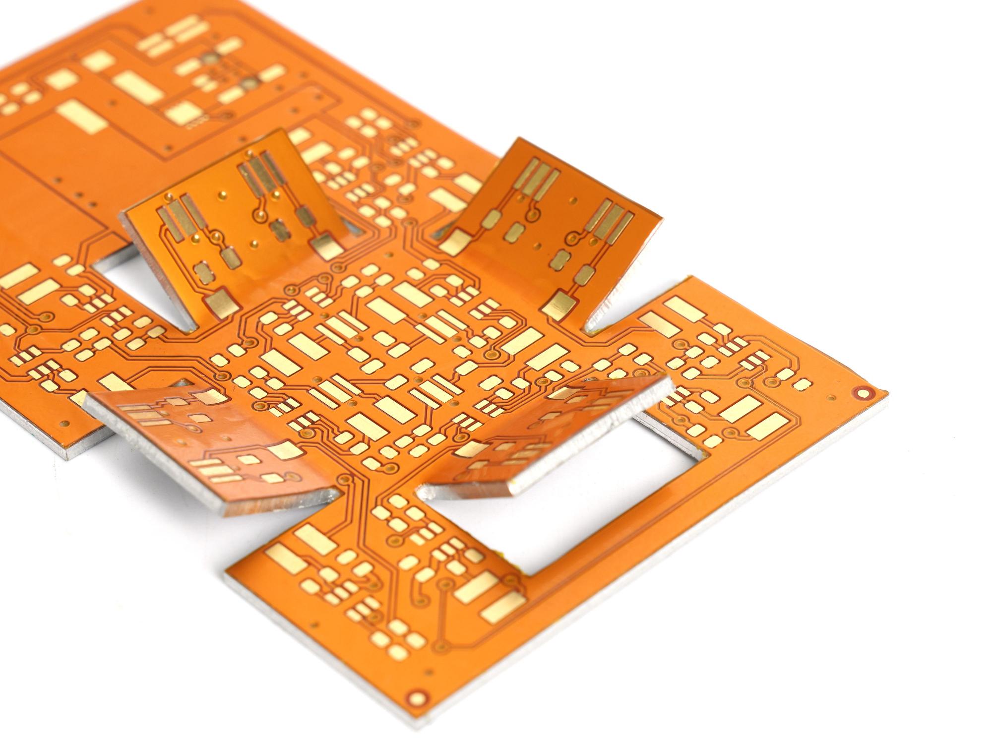
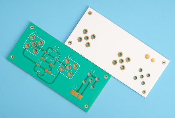
Ceramic substrate PCB is a printed circuit board with ceramic material as substrate. With its excellent performance and unique technical advantages, it occupies an important position in today’s rapidly developing electronics industry. Its high thermal conductivity, high insulation, high temperature resistance, corrosion resistance and other characteristics enable it to be widely used in many fields.

What is a ceramic substrate?

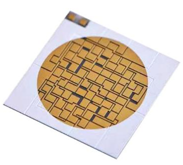
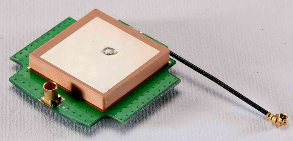
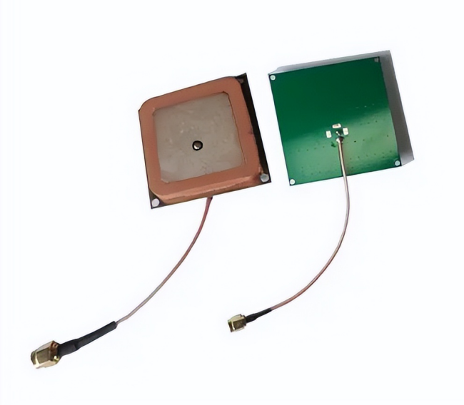
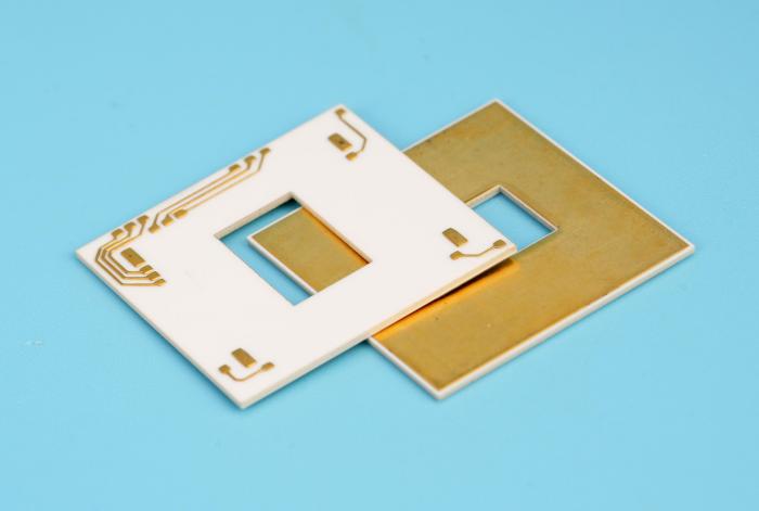
‌Ceramic substrate is a special process board in which copper foil is directly bonded to the surface (single or double sides) of alumina (Al2O3) or aluminum nitride (AlN) ceramic substrate at high temperature. ‌

What is a ceramic substrate pcb? What is it used for?

This ultra-thin composite substrate has excellent electrical insulation properties, high thermal conductivity, excellent soft solderability and high adhesion strength, and can be etched with various patterns like PCB boards, with great current carrying capacity.

Therefore, ceramic substrate has become the basic material for high-power power electronic circuit structure technology and interconnection technology.

It has a wide range of applications, including but not limited to semiconductor modules, integrated circuits and electronic ceramics, among which alumina is one of the most commonly used ceramic substrate materials.

The characteristics of ceramic substrates include strong mechanical stress, shape stability, high strength, high thermal conductivity, high insulation, strong bonding, corrosion resistance, and good thermal cycling performance, with a cycle number of up to 50,000 times and high reliability.

In addition, the operating temperature range of ceramic substrates is wide, from -55°C to 850°C, and its thermal expansion coefficient is close to that of silicon, which simplifies the production process of power modules.

How thick is a ceramic substrate?

The thickness of ceramic substrates is generally between tens and hundreds of microns. ‌ This material usually has a flat surface for connecting and supporting microelectronic components.

What is a ceramic substrate pcb? What is it used for?

The thickness of ceramic substrates can be precisely processed according to specific needs to meet different application scenarios.

The thickness of alumina ceramic substrates can be adjusted between 0.2-1.5mm, which shows that the thickness range of ceramic substrates is quite wide and can be customized according to specific application needs. ‌

What is a ceramic PCB used for?

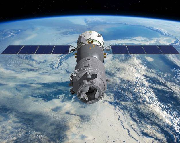
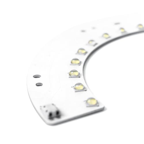
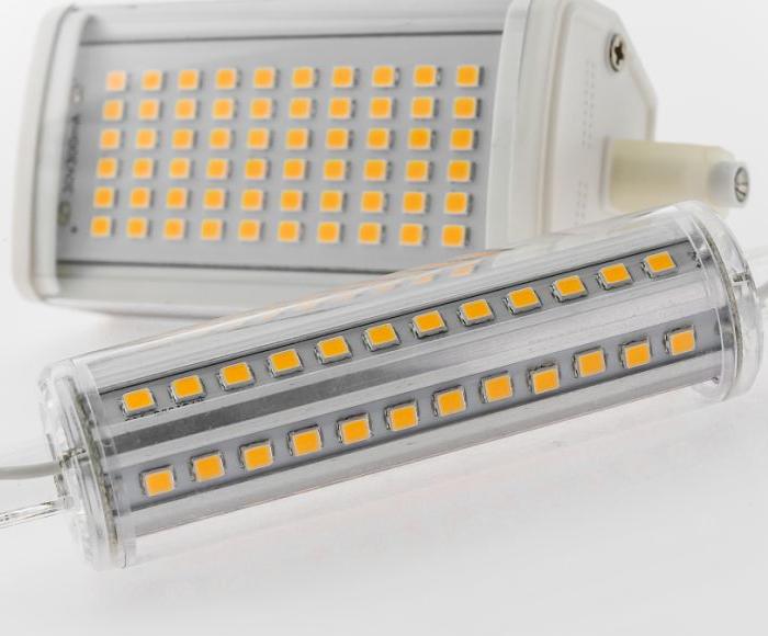
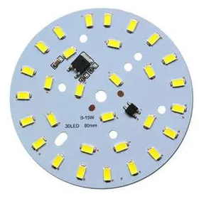
Due to its unique performance and functions, ceramic PCB is widely used in many fields, including but not limited to LED lighting, semiconductor coolers, high-power semiconductor modules, power control circuits, electronic heaters, intelligent power devices, power hybrid circuits, high-frequency switching power supplies, automotive electronics, solid-state relays, military electronics, aerospace, communications, etc.

What is a ceramic substrate pcb? What is it used for?

The requirements for electronic products in these application fields are to become thinner, smaller, and have more functions. As a new type of circuit material, ceramic PCB effectively provides a solution for the miniaturization of modern electronic products. Its advantages are:

  • Heat dissipation performance and current carrying capacity‌: The heat dissipation performance, current carrying capacity, insulation, thermal expansion coefficient, etc. of ceramic substrates are better than those of ordinary glass fiber PCB boards, and are particularly suitable for high-power power electronic modules, aerospace, military electronics and other products.
  • Thermal conductivity‌: Ceramic PCB has excellent thermal conductivity and can effectively dissipate the heat generated by components, making it the first choice for applications that generate a lot of heat and require efficient thermal management.
  • ‌Electrical performance‌: The excellent electrical performance of ceramic materials at high frequencies makes ceramic PCBs particularly suitable for radio frequency (RF) and microwave applications, which can maintain signal integrity and minimize signal loss.
  • ‌Durability and mechanical strength‌: Ceramic PCBs have impressive mechanical strength and durability, and can withstand challenging mechanical stress and vibration, while having good chemical resistance and the ability to withstand harsh environments.

In summary, ceramic PCBs occupy an important position in high-performance electronic applications due to their excellent physical and electrical properties, as well as high reliability and stability, and are an important part of the development of modern electronic technology.

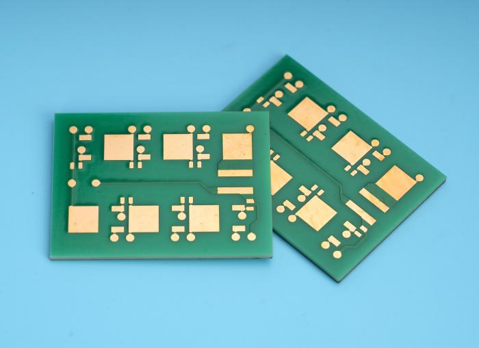
What is the difference between ceramic substrate and FR-4?

The main differences between ceramic substrates and FR-4 are their physical and electrical properties, cost, production cycle, application areas, and high-frequency performance. ‌

What is a ceramic substrate pcb? What is it used for?

‌Physical and electrical properties‌:

  • Ceramic substrates use ceramic substrates, such as alumina ceramic substrates, aluminum nitride ceramic substrates, silicon nitride ceramic substrates, etc., with good heat dissipation and insulation, thermal conductivity between 25w and 230w, and insulation resistance greater than or equal to 10 to the 14th power.
  • In contrast, FR-4 is made of glass fiber, which has poor heat dissipation performance and no insulation performance. It needs to add an insulation layer to transfer heat, and its heat dissipation performance is only a few watts.

‌Cost and production cycle‌:

  • The production cost of ceramic substrates is high, and the production cycle is usually 10~15 days.
  • In contrast, the production cost of FR-4 substrates is lower, and the production cycle is shorter. Some can be shipped in 24 hours.

‌Application areas‌:

  • Ceramic substrates are widely used in high thermal conductivity, high current, high insulation, high frequency and other fields due to their high thermal conductivity, excellent insulation, high frequency performance, high temperature resistance and corrosion resistance.
  • FR-4 substrates are more widely used and in high demand due to their low cost and short production cycle.

‌High frequency performance‌:

  • The dielectric constant of ceramic substrates is relatively stable and low, generally around 7~10, with high high frequency performance and low dielectric loss, faster and more stable signal transmission, so it is suitable for high frequency communication.
  • In contrast, the high frequency performance of FR-4 is not as good as that of ceramic substrates.

In summary, there are significant differences between ceramic substrates and FR-4 in terms of physical and electrical properties, cost, production cycle, and application areas.

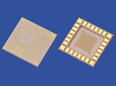
What is a ceramic substrate for power electronics?

‌The ceramic substrate for power electronics is a special process board made by directly bonding copper foil to the surface (single or double sides) of an alumina (Al2O3) or aluminum nitride (AlN) ceramic substrate at high temperature.

This ultra-thin composite substrate has excellent electrical insulation properties, high thermal conductivity, excellent soft solderability and high adhesion strength, and can be etched with various patterns like a PCB board, with a large current carrying capacity.

Therefore, ceramic substrates have become the basic materials for high-power power electronic circuit structure technology and interconnection technology.

The characteristics of ceramic substrates include strong mechanical stress, stable shape, high strength, high thermal conductivity, high insulation, strong bonding, corrosion resistance, good thermal cycle performance (cycle times up to 50,000 times, high reliability), no pollution, no pollution, wide operating temperature (-55℃~850℃), thermal expansion coefficient close to silicon, and simplified production process of power modules.

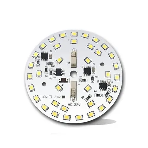
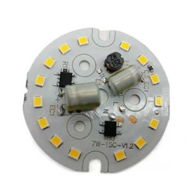
These characteristics make ceramic substrates widely used in the field of power electronics, especially in application scenarios that require high heat dissipation, low thermal resistance, long life, and voltage resistance, such as home appliance indicator lights, car lights, street lights, and large outdoor billboards.

In addition, the market for ceramic substrates is expected to increase by 94.27% in the next three years, showing a strong demand for localization. With the improvement of production technology and equipment, product prices have accelerated rationalization, further expanding its application areas in the LED industry.

The development trend of diversification and structural integration of ceramic substrates has put forward higher requirements on the performance of packaging substrates. They have been widely used in electronic device packaging, such as thin film ceramic substrates, thick film printed ceramic substrates, and direct bonding ceramic substrates. These substrates have high thermal conductivity, good heat resistance, low thermal expansion coefficient, high mechanical strength, good insulation, corrosion resistance, and radiation resistance.

Conclusion:

Ceramic substrate PCB has shown great value in the electronics industry with its excellent performance and wide range of uses. With the continuous advancement of science and technology, ceramic substrate PCB will surely be more deeply applied and developed in more fields, contributing to the innovation and progress of electronic technology.

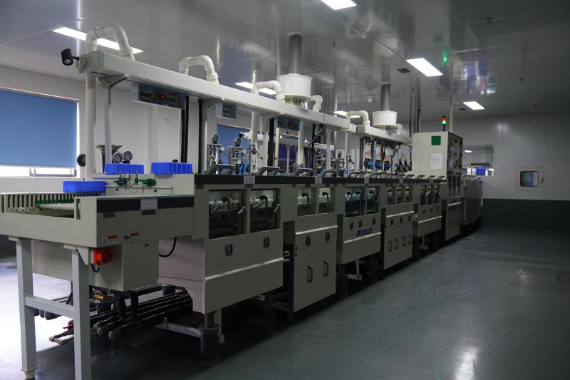
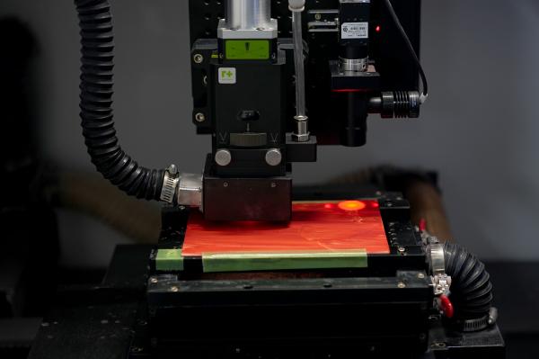
As a professional ceramic circuit board manufacturer, BEST Technology has advanced production technology and a strict quality control system. It is always committed to providing customers with high-quality products and professional services, and continuously promoting the development of the ceramic circuit board industry.

Multilayer ceramic pcb: its process and advantages
星期五, 13 9 月, 2024

As an innovative technological achievement in the field of electronics, multilayer ceramic pcb are gradually becoming a key force in promoting the development of the electronics industry. It uses ceramic materials as substrates and integrates advanced printed circuit technology, providing solid support for the miniaturization and high performance of electronic equipment.

What is a multilayer ceramic pcb?

A multilayer ceramic pcb is an electronic component that uses ceramic as a matrix material and makes metal circuits on it. It is mainly divided into planar ceramic printed circuit boards and multilayer ceramic pcb.

Planar ceramic printed circuit boards are usually used in some simple electronic devices, while multilayer ceramic pcb are widely used in multiple high-end technology fields due to their higher integration and performance.

From a classification point of view, multilayer ceramic pcb can be divided from different angles. In terms of the number of layers, ceramic circuit boards are currently dominated by single and double panels.

According to materials, there are Al2O3 ceramics, AIN ceramics and BeO ceramics.

  • Alumina substrates are commonly used substrate materials in the electronics industry, with high strength and chemical stability and abundant raw material sources.
  • AIN ceramics have high thermal conductivity and expansion coefficients that match Si, but there are relatively few domestic production technologies and the price is high.
  • Although BeO has high thermal conductivity, its development is limited by toxicity.

According to the manufacturing process, it can be roughly divided into four types: HTCC, LTCC, DBC, and DPC.

  • DBC combines Al2O3 with Cu plate by high temperature heating.
  • DPC deposits Cu on Al2O3 substrate by direct copper plating technology.
  • LTCC is also called low-temperature co-fired multilayer ceramic substrate, and HTCC is also called high-temperature co-fired multilayer ceramic.
Multilayer ceramic pcb: its process and advantages

At present, these ceramic substrates have been maturely applied to various required fields, such as cooling sheets, high-power LEDs and other industries.

What are the manufacturing processes of multilayer ceramic pcb?

Common manufacturing processes of multilayer ceramic pcb:

  • One-time sintering multilayer method: After the ceramic blank is stamped and formed, the conductive layer is printed, and then laminated or printed with an insulating layer, followed by shape punching, and finally sintered and plated with precious metals.
  • Thick film multilayer method: After the ceramic blank is stamped and sintered, the conductive layer is printed, and the conductive layer and the insulating layer are printed repeatedly, and finally sintered.
Multilayer ceramic pcb: its process and advantages
  • High temperature co-firing technology (HTCC): High temperature sintering is adopted, and the sintering temperature is usually above 1500℃. This technology can produce ceramic circuit boards with high mechanical strength, which can make the package more solid and durable. However, high melting metals such as tungsten, molybdenum, and manganese have poor conductivity and sintering shrinkage is difficult to control.
  • Low temperature co-firing technology (LTCC): Sintering at 850-900 degrees Celsius, low-capacitance capacitors, resistors, coupling and other passive components are buried in the multilayer ceramic substrate, and low-impedance metals such as gold, silver, and copper are co-fired as electrodes, and then parallel printing is used to coat the circuit.
  • Direct pressing technology (DBC): Al2O3 is combined with Cu plate by high temperature heating. The production process is relatively simple and direct, and ceramic circuit boards with certain performance can be quickly produced.
  • Vacuum sputtering technology (DPC): Cu is deposited on Al2O3 substrate using direct copper plating technology, which can produce ceramic circuit boards with high precision.

What are the application fields of multilayer ceramic pcb?

(I) Covering high-end technology fields

multilayer ceramic pcb play a vital role in the aerospace field.

Ceramic materials do not decompose chemical bonds due to heat and ultraviolet radiation, do not absorb or release moisture in large quantities, and do not outgas in extreme vacuums. They have excellent temperature resistance and high reliability.

In satellite communication systems, navigation systems, and aircraft control systems, multilayer ceramic pcb ensure that circuits work stably in extreme environments.

Multilayer ceramic pcb: its process and advantages

In the field of medical equipment, multilayer ceramic pcb are widely used in imaging equipment and life support systems. The multilayer design can integrate more functions in a limited space, meeting the key needs of portable medical devices and compact designs.

In the field of automotive electronics, as cars develop towards electronicization and intelligence, the use of multilayer ceramic pcb is becoming more and more common. From engine management systems to entertainment systems, it improves circuit reliability, reduces weight, and improves overall performance.

In communication systems, especially in data centers and network equipment, multilayer ceramic pcb are widely used due to their superior signal integrity and electromagnetic interference shielding capabilities. High-speed signal transmission is possible while ensuring the quality and stability of data transmission.

In the field of high-performance computing, the high integration and high performance of multilayer ceramic pcb can meet the needs of large-scale data processing and high-speed computing.

(II) Significant advantages are widely used

multilayer ceramic pcb have a high degree of integration and can arrange more components and circuits in a limited space to achieve more complex circuit designs.

It has extremely high reliability and adopts professional manufacturing processes with good electrical and mechanical properties. Through strict quality control and testing, the stability and reliability of the circuit board are guaranteed.

Strong design flexibility allows more complex circuit layouts, providing space for innovation and technological progress. Designers can optimize circuit design and reduce the length of signal paths, thereby speeding up signal transmission.

What are the unique advantages of multilayer ceramic pcb?

(I) Excellent performance

multilayer ceramic pcb have many excellent properties. First, high thermal conductivity enables them to dissipate heat quickly and effectively, ensuring that electronic components maintain a stable temperature during operation.

The good thermal expansion coefficient makes the thermal expansion coefficient of the ceramic circuit board similar to that of the chip, which can reduce the impact of thermal stress on the chip. When the temperature changes, the thermal stress between the circuit board and the chip is reduced, which improves the reliability and service life of the electronic equipment.

The low-resistance metal film layer ensures good conductivity and reduces the loss of signal transmission.

The substrate has good solderability, which is convenient for the installation and welding of electronic components and improves production efficiency. Good insulation can effectively prevent circuit short circuits and ensure the safe operation of electronic equipment.

The low high-frequency loss makes the multilayer ceramic pcb have significant advantages in the field of high-frequency communication. In high-frequency signal transmission, the signal loss is low, which can ensure the quality and stability of the signal.

The high-density assembly feature enables the ceramic circuit board to integrate more electronic components in a limited space and realize more complex circuit design.

(II) Rich types suitable for different scenarios

  • Aluminum nitride ceramic circuit boards have the advantages of high thermal conductivity and expansion coefficient matching Si. Its high thermal conductivity can quickly dissipate the heat generated inside the device, making it an ideal packaging material for high-power electronic devices. In the field of high-power LED lighting, aluminum nitride ceramic circuit boards can provide good heat dissipation performance and extend the service life of LED lamps.
  • Alumina ceramic circuit boards are more common, cost-effective, with good insulation and moderate thermal conductivity. Alumina substrates are commonly used substrate materials in the electronics industry, with high strength and chemical stability, abundant raw material sources, and are suitable for a variety of technical manufacturing and different shapes.
  • Thick film ceramic circuit boards consist of gold and dielectric paste printed on a ceramic substrate and baked at a temperature slightly below 1000°C. Thick film ceramic PCBs can use gold or copper, and copper is used most due to its lower cost.
  • LTCC has excellent high frequency, high Q characteristics and high-speed transmission characteristics, good temperature characteristics, can adapt to high current and high temperature resistance requirements, easy to achieve multi-functionality and improve assembly density, and high reliability.
  • High temperature co-fired ceramic (HTCC) circuit boards use alumina and adhesives as well as plasticizers, solvents and lubricants. This method is most suitable for small circuit boards and carrier circuits. HTCC has the advantages of high mechanical strength, high wiring density, and stable chemical properties.

What is the future development of multilayer ceramic pcb?

(I) The market size continues to grow

In recent years, the market size of my country’s ceramic circuit board industry has shown a trend of continuous growth. According to statistics, the market size will be about 2.399 billion yuan by 2023, and the CAGR from 2015 to 2023 will be 19.1%. With the continuous development of the electronic information industry, the market demand for ceramic circuit boards as key electronic components will continue to grow.

(II) Technological progress drives development

With the rapid development of the new generation of information technology, downstream demand will inevitably be more diversified and more technologically advanced, which will put forward higher requirements on the R&D level and process level of ceramic circuit board industry manufacturers.

The downstream industries include integrated circuit packaging, LED, automotive electronics, aerospace and military electronic components. The scale development of the downstream market has created considerable new market capacity for the ceramic circuit board industry. At the same time, the structural upgrading of the downstream industry will help the technological progress of the ceramic circuit board industry.

(III) The global market has broad prospects

In 2023, the global multilayer printed circuit board market size is about 168.8 billion yuan, and it is expected that the market size will be close to 192.9 billion yuan by 2030, with a CAGR of 1.9% in the next six years.

At present, China is the world’s largest market for multilayer printed circuit boards, accounting for nearly 60% of the market share. From the perspective of the global market competition landscape, the sales volume, revenue, price market share and industry ranking of multilayer printed circuit boards of leading companies in the global market are constantly changing.

Conclusion:

In short, multilayer ceramic pcb have shown great potential in the electronics industry with their unique advantages. With the continuous advancement of science and technology, it will play a more key role in more fields and continue to inject new vitality into the innovation and development of electronic technology. BEST Techbology has always been committed to providing customers with high-quality products and professional services, and continuously promoting the development of the ceramic circuit board industry.

Differences Guide, ceramic antenna vs pcb antenna
星期四, 12 9 月, 2024

Antenna plays a vital role in wireless devices, and ceramic antenna and PCB antenna have their own characteristics. Ceramic antenna is small, low cost, easy to use, and has good anti-interference, waterproof, dustproof, lightning protection and other properties. PCB antenna is an important RF component and is also indispensable in wireless communication equipment.

What is a ceramic antenna?

Ceramic antenna is a miniaturized antenna suitable for Bluetooth devices. It uses a ceramic shell and has anti-interference, lightning resistance, waterproof and dustproof capabilities.

Differences Guide, ceramic antenna vs pcb antenna

It mainly uses GPS satellites to achieve navigation and positioning. It is divided into block ceramic antenna and multilayer ceramic antenna. Block antenna uses high temperature to sinter the entire ceramic body once and then prints the metal part of the antenna on the surface of the ceramic block.

Multilayer antenna firing uses low temperature co-firing to stack and align multiple layers of ceramics and then sinter at high temperature. The metal conductor of the antenna can be printed on each layer of ceramic dielectric layer according to design requirements, which can effectively reduce the size of the antenna and achieve the purpose of hiding the antenna.

Since the dielectric constant of ceramic itself is higher than that of PCB circuit board, and the dielectric loss is also smaller than that of PCB circuit board, the use of ceramic antenna can effectively reduce the size of antenna while ensuring antenna performance, and is more suitable for use in low-power Bluetooth modules.

Ceramic antennas are widely used in Bluetooth devices, such as Bluetooth headsets, smart watches, Bluetooth e-cigarettes, smart small appliances, smart medical, smart home products, etc. Its gain is generally 2dbi, and the reading distance can reach 2 meters. It is an industrial-grade product for indoor use, with an external size of 78mm×78mm×5mm.

What is a PCB antenna?

PCB antenna refers to the part on the PCB used for wireless reception and transmission.

Differences Guide, ceramic antenna vs pcb antenna

When transmitting, it converts the high-frequency current of the transmitter into electromagnetic waves in space; when receiving, it converts the electromagnetic waves intercepted from space into high-frequency current and sends them to the receiver. Usually set on Bluetooth or wireless transmission modules. For example, PCB antennas play an important role in ZM602 series Wi-Fi modules, achieving performance indicators such as gain > 2.0dBi, working bandwidth > 150MHz, S11 within bandwidth < -10dB, input impedance 50Ω, and standing wave ratio < 2.0.

The most common structure of PCB antenna is the inverted F antenna. The length of the antenna needs to meet the quarter free space wavelength of the transmitted signal. In actual design, it is often designed as a serpentine trace to reduce the occupied space.

The advantages of PCB antennas are small space occupation, low cost, no need to assemble the antenna separately, not easy to touch and damage, and convenient assembly of the whole machine; the disadvantages are that it is difficult to make a single antenna field round, the insertion loss is high, the efficiency is relatively low, and it is easy to be interfered by the motherboard.

What are the differences between ceramic antennas and PCB antennas?

  • (I) Difference in dielectric constant:

In terms of dielectric constant, ceramic antennas have obvious advantages. The dielectric constant of ceramic antennas is higher than that of PCB antennas, which enables ceramic antennas to gather and transmit electromagnetic wave signals more effectively.

The higher dielectric constant allows ceramic antennas to be more compact in design, effectively reducing the size of the antenna. In some miniaturized Bluetooth devices, such as smart watches and Bluetooth headsets, the high dielectric constant characteristics of ceramic antennas can meet the strict space requirements of the device, leaving more design space for other electronic components.

  • (II) Difference in dielectric loss:

Ceramic dielectrics also perform well in dielectric loss. Compared with PCB circuit boards, ceramic dielectrics have lower dielectric losses, which means that in low-power Bluetooth modules, ceramic antennas can transmit signals more efficiently while reducing energy loss.

The use of ceramic antennas in low-power Bluetooth modules is significantly better than PCB antennas, which can effectively extend the battery life of Bluetooth devices. The low dielectric loss characteristics of ceramic antennas can ensure that the device still maintains stable signal transmission when running for a long time.

  • (III) Difference in size and effect:

The size of ceramic antennas is generally comparable to that of 1210 packages. In practical applications, antennas of this size can well meet the design requirements of various miniaturized electronic devices. At the same time, the effect of ceramic antennas is stronger than that of PCB antennas. This is because the special structure and material properties of ceramic antennas make them more efficient and stable in signal reception and transmission.

In some Bluetooth audio devices with high signal quality requirements, ceramic antennas can provide clearer and more stable audio transmission effects, reducing signal interference and distortion. However, due to the limitations of its design and manufacturing, PCB antennas are often not as good as ceramic antennas in signal transmission effects.

What are the benefits of ceramic antennas?

Advantages:

Ceramic antennas take up little space, which makes them very advantageous in miniaturized electronic devices. For example, in wearable devices such as smart watches and Bluetooth headsets, more space can be left for other electronic components, making the design of the device more compact.

Its performance is good, and it can effectively reduce power consumption while ensuring signal strength. For example, in some low-power Bluetooth devices, ceramic antennas can extend the battery life of the device.

Ceramic antennas can also effectively improve the integration of the motherboard, reduce the antenna’s restrictions on ID, and introduce the design in the early stage of product design, so that it can be better integrated with the motherboard and improve the overall performance of the product.

Disadvantages:

The bandwidth of ceramic antennas is narrow, and it is difficult to achieve multi-band. This means that in some application scenarios that need to support multiple frequency bands at the same time, ceramic antennas may not meet the needs.

In some multifunctional wireless communication devices, it is necessary to support multiple frequency bands such as Bluetooth, Wi-Fi, GPS, etc. at the same time. Ceramic antennas may need to be used in conjunction with other antennas, which increases the complexity and cost of the design.

What are the benefits of PCB antennas?

Advantages:

PCB antennas take up less space and are especially suitable for electronic devices that have strict space requirements. For example, in some ultra-thin smartphones and laptops, PCB antennas can be directly integrated on the circuit board without taking up additional space.

Low cost is also an important advantage of PCB antennas. Since it can be made directly on the PCB board, no additional assembly process is required, which reduces production costs.

PCB antennas do not need to be assembled separately, are not easily damaged by touch, and are easy to assemble as a whole, which improves production efficiency.

Disadvantages:

It is difficult to make a single antenna field of a PCB antenna round, which will affect the coverage and stability of the signal.

High insertion loss means that the signal is lost more during transmission, reducing the strength and quality of the signal.

PCB antennas are easily interfered by other electronic components on the motherboard, which requires careful consideration and optimization during design and layout to reduce the impact of interference on the signal.

Application scenarios and selection of ceramic antennas and PCB antennas

According to different needs, PCB onboard antennas can be selected in environments without metal coverage, IPEX external antennas can be selected with metal coverage, and ceramic antennas can be selected if the space is not large.

Differences Guide, ceramic antenna vs pcb antenna

In actual applications, different usage environments and needs determine the choice of antenna type. If it is in an environment without metal coverage, PCB onboard antennas are an economical and convenient choice. PCB onboard antennas have the advantages of low cost, no need to assemble antennas separately, not easy to touch and damage, and easy assembly.

When in an environment with metal coverage, IPEX external antennas are more suitable. IPEX external antennas have good directional directivity, high efficiency, strong anti-interference ability, and can stay away from interference on the motherboard. Although it is costly and difficult to assemble, it can ensure stable signal transmission in a metal environment.

If the PCB board space is not large, ceramic antennas are an ideal choice. Ceramic antennas can effectively reduce the size of the antenna to achieve the purpose of hiding the antenna. At the same time, since the dielectric constant of ceramic itself is higher than that of PCB circuit board, it can better adapt to the design requirements of small space while ensuring performance.

In summary, when choosing an antenna, we need to comprehensively consider the specific use environment and needs and choose the most suitable antenna type to ensure that the device can achieve stable and efficient wireless communication.

Conclusion:

Ceramic antennas and PCB antennas each have their own characteristics and advantages. Understanding their differences will help you make the most appropriate decision when choosing wireless devices.

BEST Technology has many years of experience in manufacturing ceramic circuit boards. Its products can provide stable and reliable signal transmission in the fields of GPS navigation, Bluetooth devices, wireless LAN, and the Internet of Things.

Ceramic PCB Manufacturers: Development History and Future
星期四, 12 9 月, 2024

In today’s era of rapid technological development, ceramic PCBs have emerged in many fields with their excellent performance and unique advantages. Behind ceramic PCBs are a group of professional ceramic PCB manufacturers who are promoting the progress and development of the electronics industry with their unremitting efforts and superb skills.

Ceramic PCB Manufacturers: Development History and Future

Reasons for the development of ceramic pcb manufacturer

  • (I) Expansion of market size

In recent years, the ceramic PCB market size has shown a growing trend. According to statistics, the global ceramic substrate market size reached US$1.13 billion in 2022 and is expected to reach US$4.15 billion in 2029, with a compound annual growth rate (CAGR) of 18.23%.

In the Chinese market, the market size of China’s ceramic circuit board industry is about 2.399 billion yuan by 2023, with a CAGR of 19.1% from 2015 to 2023.

In terms of output, China’s ceramic substrate output accounted for about 35.9% of the world’s total in 2022, and is expected to reach 54.9% in 2029. Europe is the second largest market region, with a share of 33% in 2022 and an estimated 21.99% in 2029. Japan, Southeast Asia, South Korea and Taiwan are also important production areas.

  • (II) Promotion of technological progress

Technological innovation plays a vital role in promoting ceramic PCB manufacturers. In terms of the application of new materials, the research and development of new ceramic materials provides more options for ceramic PCBs.

In terms of production process improvements, ceramic PCB manufacturing technology includes steps such as pressing, welding, metallization and printing. By optimizing process parameters and process control, higher quality ceramic PCBs can be obtained.

The application of laser cutting and punching technology in the production of ceramic circuit boards improves processing accuracy and speed, and meets the requirements of small size and high density of electronic devices and semiconductor components.

What are the well-known ceramic pcb manufacturers?

BEST Technology:

  • Product features: A domestic manufacturer that focuses on the R&D and production of large, medium and small batches of ceramic circuit boards and prototypes, serving high-tech enterprises and scientific research institutions at home and abroad. Mainly focused on MCPCB, FR4 PCB, Ceramic PCB, Special PCB such as Heavy Copper (up to 20 OZ), and PCB assembly service.
  • Market share: Ranked among the top domestic ceramic substrate manufacturers, with a monthly production capacity of 100,000 sheets.
Ceramic PCB Manufacturers: Development History and Future
  • Technical advantages: Over 18 years of experience in the PCB industry. Proficient in DPC, AMB, DBC, LTCC, HTCC production processes, fully passed TS16949, ISO9001, ISO14001 certification. With the aim of “zero quality defects”, we provide high-quality products and services, with short delivery time and stable quality for ceramic boards.

What are the production processes of ceramic PCBs?

(I) Laser processing technology

Lasers play a vital role in ceramic PCB processing. Laser drilling has the advantages of high precision and high efficiency, and can meet the requirements of electronic devices and semiconductor components for micropore diameters ranging from 0.05 to 0.2 mm.

Ceramic PCB Manufacturers: Development History and Future

Laser cutting also has many advantages. First, it has high precision, fast speed, narrow slits, small heat-affected zone, and smooth cut surfaces without burrs.

(II) Other molding processes

  • Tape casting: The advantage is that it can produce large-area, thin-thickness and uniform ceramic substrates, which are suitable for large-scale production. However, tape casting has high requirements for equipment, and the viscosity and fluidity of the slurry need to be controlled during the process.
  • Powder pressing: Simple operation and low cost. However, the pressed ceramic substrate may have problems of uneven density and high porosity, which affect its performance.
  • Extrusion molding: Suitable for the production of long strip or tubular ceramic substrates with high production efficiency. However, the shape of the extruded ceramic substrate is relatively simple and the dimensional accuracy is relatively low.

(III) LAM process advantages

The LAM process has significant advantages in ceramic PCB manufacturing.

First, the bonding strength between the metal layer and the ceramic is high, up to 45 MPa (the strength of the ceramic sheet is greater than 1mm thick), the conductivity is good, and the heat is small when the current passes through.

Secondly, the thermal conductivity is high. The thermal conductivity of alumina ceramics is 20-35 W/mk, and the thermal conductivity of aluminum nitride ceramics is 170-230 W/mk, which is much higher than the thermal conductivity of the traditional aluminum-based circuit board MCPCB of 1 to 2 W/mk.

In addition, the insulation is good, and the breakdown voltage is as high as 20KV/mm. The thickness of the conductive layer can be customized arbitrarily within the range of 1μm-1mm, and the current can be designed according to the circuit module. The thicker the copper layer, the greater the current passing through.

The high-frequency loss is small, and high-frequency circuits can be designed and assembled; the dielectric constant is very small, and the line/spacing (L/S) resolution can reach 20μm, thus achieving short and thin devices.

It does not contain organic components, is resistant to cosmic rays, and has high reliability and long service life in the aerospace field; the copper layer does not contain an oxide layer and can be used for a long time in a reducing atmosphere.

What are the characteristics of ceramic pcb manufacturer?

  • (I) Obvious technical advantages

Ceramic PCB manufacturers have significant technical advantages. First of all, high thermal conductivity is one of the outstanding features of ceramic PCB. This enables ceramic PCB to effectively dissipate heat in high-power electronic equipment and improve the reliability and stability of the equipment.

Low thermal expansion coefficient is also an important technical feature of ceramic PCB. Its thermal expansion coefficient is close to that of silicon chips, which can save labor and materials and reduce costs. At the same time, when the temperature changes, it can reduce the stress caused by thermal expansion and contraction, and ensure the stability of the circuit.

High surface hardness makes ceramic PCB more durable and longer service life. Compared with traditional PCBs, ceramic PCBs are not easily scratched and worn, and can maintain good performance in harsh environments.

  • (II) Adapt to a variety of fields

Ceramic PCB has a wide range of application advantages in many fields.

In the field of LED lighting, the excellent heat dissipation performance of ceramic PCB can effectively reduce the temperature of LED chips, improve luminous efficiency and life. At the same time, ceramic PCB has good insulation and high pressure resistance, which ensures personal safety and equipment protection.

Ceramic PCB Manufacturers: Development History and Future

In the semiconductor field, the high thermal conductivity of ceramic PCB can quickly conduct heat away from semiconductor chips and improve cooling efficiency. In addition, the low thermal expansion coefficient and high surface hardness of ceramic PCB can adapt to the working environment of semiconductor coolers at different temperatures and ensure its stable performance.

  • (III) Clear market structure

At present, the ceramic PCB market presents a clear competitive pattern. In the global market, a few internationally renowned companies occupy a large market share. These companies have advanced technology and rich experience, and have strong strength in material research and development, production technology and market expansion.

The development opportunities for domestic manufacturers lie in the huge demand and policy support of the domestic market. With the rapid development of strategic emerging industries such as 5G communications, new energy vehicles, and high-end manufacturing, the market demand for ceramic PCBs will continue to grow.

At the same time, domestic manufacturers are also facing some challenges. On the one hand, international competitors have strong technical strength and brand influence, and domestic manufacturers need to increase investment in technological innovation and brand building. On the other hand, the production cost of ceramic PCBs is high, and domestic manufacturers need to continuously optimize production processes, reduce costs, and improve the cost performance of products.

What is the market prospect of ceramic PCB manufacturers?

(I) Strong policy support

As the core material of passive electronic components, electronic ceramics are an important material basis for electronic information technology.

In order to promote the development of the electronic ceramics industry, the state has issued a series of policies, such as “Opinions on Deepening the Reform of the Management System of the Electronic and Electrical Industry”, “The 14th Five-Year Plan for the Development of the Digital Economy”, “The 14th Five-Year Plan for the Development of Intelligent Manufacturing”, and “The 14th Five-Year Plan for the Development of China’s Electronic Components Industry”.

At the same time, the state has also strengthened quality management supervision of the PCB board industry, formulated strict quality standards and testing requirements, and supported enterprises to carry out ISO quality management system certification to improve product quality and competitiveness.

In terms of environmental protection, the Chinese government has adopted strict environmental protection policies to regulate the production and processing processes of the PCB board industry, restrict the use of hazardous substances, promote the recycling of resources and promote clean production, laying a solid policy foundation for the development of ceramic PCB manufacturers.

(II) Market demand growth

With the rapid development of downstream application fields such as new energy vehicles and 5G communications, the market demand for ceramic PCBs has shown a strong growth trend.

In the field of new energy vehicles, a large number of high-voltage and high-power devices contained in new energy vehicles, such as IGBT and MOSFET, have high requirements for heat dissipation.

Ceramic substrates have a good heat dissipation effect, which can dissipate the high heat in the power system in time to ensure the normal operation of large power loads, further increasing the use of PCBs for new energy vehicles.

In the field of 5G communications, the advent of the 5G era has made signal base stations more dense, with the number reaching 100 times that of 4G, including a series of software and hardware upgrades brought about by the iterative upgrade of terminal receiving devices.

As hardware for high-frequency transmission, the core of it is the circuit board. At present, the circuit board with the smallest transmission loss is the ceramic circuit board, which has long been widely used in the communications industry.

In the future, entering 2020, 5G will be expected to be commercially available. With the development of the new era of 5G, it is expected that by 2030, the domestic direct economic output will reach 6.3 trillion, and 8 million jobs will be created.

(III) Future development trends

  • Technological innovation: Ceramic PCB manufacturers will continue to increase their technological innovation efforts, develop new ceramic materials and advanced production processes.
  • Product upgrade: With the continuous improvement of PCB performance requirements in downstream application fields, ceramic PCB manufacturers will launch higher-end and more personalized products.
  • Market expansion: Ceramic PCB manufacturers will actively expand domestic and foreign markets, strengthen cooperation with downstream customers, and increase the market share of products. In the international market, domestic manufacturers can enhance brand awareness and influence and expand overseas markets by participating in international exhibitions and cooperating with internationally renowned companies.
How does solder paste inspection work?
星期二, 10 9 月, 2024

In the field of electronic manufacturing, precision is the key. One of the key processes is to ensure that the solder paste applied to the circuit board is in the correct position and in the correct amount. This process is called solder paste inspection (SPI) and plays a key role in the reliability of electronic products.

In the SMT patch process, solder paste inspection is the first and most important step, which determines the subsequent soldering quality and other issues, so the solder paste inspection step is crucial.

How to check solder paste?

1. Visual observation:

Under natural light or good lighting conditions, directly observe the appearance characteristics of the solder paste such as color and state with the naked eye. Normal solder paste has uniform color and no obvious particle agglomeration, precipitation, stratification and other phenomena.

How does solder paste inspection work?

2. Viscosity detection:

Viscosity is an important physical performance indicator of solder paste, which has a great influence on printing performance and welding quality. Professional equipment such as rotary viscometer can be used for detection.

In general, the viscosity of solder paste should be within a certain range and meet the product specification requirements. If the viscosity is too high, it may cause printing difficulties and poor demolding; if the viscosity is too low, the solder paste may flow during printing, affecting printing accuracy.

3. Metal content detection:

Metal content directly affects the welding performance of solder paste and the strength of solder joints. Chemical analysis or spectral analysis is usually used for detection.

4. Particle size detection:

The particle size and distribution of metal particles in solder paste will also affect its performance. Laser particle size analyzer and other equipment can be used for detection.

This method determines the particle size distribution of particles by measuring the scattering or diffraction of metal particles on laser. Generally, the particle size distribution of metal particles is required to be concentrated within a certain range, and the proportion of particles that are too large or too small should not be too high.

What is the most common solder paste?

The most common solder paste is rosin solder paste.

‌Rosin solder paste is widely used because of its excellent flux and protective effect, as well as the protective film formed after welding, which has a protective effect on solder joints. Even if cleaning is not required, there will be no corrosion.

In addition, rosin is easy to mix with other ingredients, which can play a role in adjusting viscosity, so that the metal powder in the solder paste is not easy to precipitate and stratify. These characteristics make rosin solder paste the most common type of solder paste.

What are the advantages of solder paste inspection?

Solder paste inspection has many advantages, as follows:

1. Ensure product quality:

  • Discover problems in advance: By inspecting solder paste before welding, you can find quality problems of the solder paste itself in time, such as uneven composition, inappropriate metal particle size, insufficient flux activity, etc., to ensure the welding quality of electronic products from the source.
  • Optimize welding process: By testing the viscosity, thixotropy and other performance indicators of solder paste, you can determine whether the solder paste is suitable for the current printing process and welding equipment.

2. Improve production efficiency:

  • Reduce rework of defective products: Testing solder paste can quickly screen out solder paste that does not meet quality requirements and avoid using these solder pastes in production, thereby reducing defective products caused by solder paste quality problems.
  • Easy to control the production process: In large-scale production, you can regularly test the solder paste, monitor the quality changes of the solder paste in real time, and detect abnormal conditions in the production process in time.

3. Reduce production costs:

  • Avoid material waste: By testing the solder paste, you can avoid using problematic solder paste, reduce material waste and unnecessary production costs.
  • Extend equipment life: Good quality solder paste can reduce wear and corrosion on printing equipment and welding equipment, and reduce equipment maintenance costs and replacement frequency.

4. Meet industry standards and customer requirements:

  • Meet industry specifications: The electronics industry has strict standards and specifications for welding quality, such as IPC standards. Conducting solder paste inspection can ensure that the quality of solder paste meets the requirements of these standards and specifications and improve the competitiveness of enterprises.
  • Meet customer needs: In the production process of electronic products, customers usually have clear requirements for welding quality. Through solder paste inspection, improve customer trust and satisfaction with the company and enhance the market competitiveness of the company.

What are the defects of solder paste inspection?

Although solder paste inspection is a key step, it is not without challenges. Some common defects found during SPI include:

  • Insufficient solder paste: If too little solder paste is used, it will result in fragile joints or poor electrical connections.
  • Too much solder paste: Too much solder paste can cause bridging between components, causing short circuits.
How does solder paste inspection work?
  • Misalignment: If the solder paste is not applied accurately, it may not align with the pads on the PCB, causing problems when placing components.
  • Collapse: In some cases, solder paste may spread too much after application, resulting in poor joint formation.
  • Solder balls: Small, unwanted solder balls may form around the pad, which may cause electrical shorts.

Do you need flux when using solder paste?

Additional flux is usually not required when using solder paste.

Solder paste itself contains flux ingredients. Solder paste is a paste-like substance made by evenly mixing solder alloy powder and flux. The role of flux in solder paste mainly includes removing oxides on the soldering surface, reducing the surface tension of solder, and promoting solder wetting and diffusion.

During the soldering process, the flux in the solder paste will work at the appropriate temperature to help achieve good soldering results. However, in some special cases, such as soldering some special materials or when there are extremely high requirements for soldering quality, additional flux may be considered, but this is a relatively special application scenario.

What is a solder paste inspection machine?

Solder Paste Inspection (SPI) is a device used to detect solder paste printed on a printed circuit board (PCB).

How does solder paste inspection work?

The main functions include:

1. Solder paste height measurement

  • Use laser scanning, optical imaging and other technologies to accurately measure the height of solder paste on the PCB pad.

2. Solder paste area measurement

  • Determine the coverage area of ​​solder paste on the pad. If the solder paste area is too small, a good solder connection may not be guaranteed; if the area is too large, it may overflow the pad, affecting the subsequent assembly process.

3. Volume measurement

  • Calculate the volume of solder paste based on height and area data. Accurate volume measurement helps ensure consistent solder paste volume for each solder joint, thereby improving the stability of soldering quality.

4. Defect detection

  • Misprint detection: Detect whether there is solder paste misprint on the PCB pad.
  • Offset detection: Detect whether the solder paste printing position is offset from the designed pad position.
  • Shape anomaly detection: Identify whether the shape of the solder paste is abnormal, such as irregular shape, unclear edges, etc. Shape anomalies may be due to problems in the printing process, which will affect the welding quality.

Solder paste inspection machines can detect solder paste quality problems in the printed circuit board production process in a timely manner, improve production efficiency and product quality, and reduce rework and scrap caused by poor soldering.

What is the best temperature for solder paste?

The optimal temperature range for solder paste is 150℃~180℃‌, and the time to maintain this temperature range should be 60~120 seconds to ensure that the solder paste can fully infiltrate the pads and component pins.

This temperature and time range is critical to controlling the quality of reflow soldering, as it involves the effective volatilization of flux and the full infiltration of pads, thereby ensuring the reliability and quality of soldering‌.

Conclusion:

Solder paste inspection is a key step in modern electronic manufacturing to ensure that solder paste is correctly and evenly applied to PCBs. By using advanced SPI machines, defects can be detected early, process control can be improved, and costs can be reduced. Whether using leaded or lead-free solder paste, ensuring the correct amount, alignment, and temperature is critical to forming strong and reliable solder joints.

BEST Technology has a professional solder paste inspection machine. Each PCB board must undergo rigorous testing. Choosing BEST Technology, you will get the highest quality PCB board.

Will the silver on the PCB oxidize?
星期二, 10 9 月, 2024

Silver is widely used in printed circuit boards (PCBs) for its excellent conductivity and thermal properties. A common concern of manufacturers is whether silver will oxidize over time, which may affect the performance of the PCB. And how should it be treated after oxidation? How should it be stored during use, etc.

How to remove oxidation from PCB?

The methods for removing oxides from PCBs mainly include physical cleaning, chemical cleaning, and mechanical polishing.

Will the silver on the PCB oxidize?

1. ‌Physical cleaning‌:

Use alcohol or diluent to gently wipe the oxidized part until the oxide is removed. This method is suitable for removing the surface oxide layer, but it is not suitable for situations where the metal surface circuit has been damaged.

2. ‌Chemical cleaning‌:

Use specific cleaning agents such as deionized water, isopropyl alcohol, acetone, etc. to effectively remove residues and contamination.

In addition, cleaning and corrosion using acidic solutions or oxidants is also an effective chemical method, but it must be used with caution to avoid damage to the PCB board and other components.

3. ‌Mechanical polishing‌:

Use fine sandpaper or abrasive cloth to carefully polish the oxidized area to restore the conductivity of the metal. This method is suitable for removing thicker oxide layers, but you need to control the strength to avoid damaging the pad surface.

Before any cleaning and repair, be sure to disconnect the PCB power supply to ensure safety. For cases where oxidation has damaged the metal surface circuit, conductive paint needs to be used for repair, but be aware that excessive use of conductive paint may damage the circuit board. In addition, for unused PCBs, they should be stored in sealed bags or protective agents and checked regularly to ensure that they are not oxidized again.

Is silver oxidation permanent?

Silver oxidation is not permanent. ‌

Will the silver on the PCB oxidize?

Silver oxidation is caused by the reaction of silver with chemicals such as oxygen and sulfur in the air, resulting in a black silver sulfide film on the silver surface. This oxidation reaction is one of the main reasons for the blackening of PCBs.

However, silver oxidation is not permanent, because the oxide layer can be removed by cleaning and maintenance to restore the gloss of the PCB surface. For example, regular use of professional PCB cleaners or soaking the PCB in diluted detergent water, then gently scrubbing it with a soft brush, and finally rinsing it with clean water and drying it can effectively remove the oxide layer.

In addition, avoiding contact with chemicals, keeping dry, regularly checking and properly storing PCBs are also effective ways to prevent oxidation.

Therefore, although silver oxidation is inevitable, the rate of oxidation can be slowed down through proper care and maintenance.

What is the best way to Deoxidize silver?

The best way to remove silver oxide from PCBs is to use chemical stripping, which involves using a specific chemical solution to treat the silver plating so that it dissolves in the solution to achieve the purpose of removing the oxide.

The effectiveness of this method depends on the selection of appropriate chemical formulas and operating conditions to ensure that the silver layer can be completely stripped while avoiding corrosion to the base metal.

In chemical stripping, different formulas can be used to achieve the removal of the silver layer. For example, one formula includes a mixture of concentrated sulfuric acid and concentrated nitric acid, which is used at a temperature of 80°C until the silver layer is completely stripped.

Another formula includes a mixture of sulfuric acid, nitric acid, silver chloride and potassium cyanide, which is also used at a temperature of 80°C. These formulas need to be selected according to actual conditions, and attention should be paid to safety measures during operation to prevent corrosion of the base metal.

In addition, for the oxidation problem of PCB gold fingers, although it is not exactly the same as the method of removing silver oxide, some cleaning methods are provided, such as using erasers, alcohol cleaning, decontamination paste cleaning, scrubbing board grinding and electroplating treatment, which are also suitable for treating silver oxide, especially when the oxide is relatively mild.

In summary, the best way to remove PCB silver oxide is chemical stripping, which is achieved by selecting appropriate chemical solutions and operating conditions. For more serious oxidation situations, it may be necessary to combine physical and chemical methods for cleaning.

How do you save silver from oxidation?

The methods to prevent PCB silver from oxidation mainly include the following points:

  • Reasonable storage and packaging ‌: During storage and transportation, PCBs should be stored in a dry, ventilated, dust-free environment to avoid moisture and corrosion. Use appropriate packaging materials, such as moisture-proof bags, foam boxes, etc., to ensure the integrity and quality of the PCB.
Will the silver on the PCB oxidize?
  • ‌Surface treatment ‌: During the PCB surface treatment process, surface treatment methods such as gold plating and tin plating can be used to prevent oxidation.
  • Use anti-oxidation coating ‌: Anti-oxidation coating is an efficient and reliable method to prevent PCB oxidation. It can form a strong, corrosion-resistant protective layer on the surface of the PCB, effectively preventing the PCB from being damaged by oxidation.
  • Reduce contact with air and moisture‌: Make sure the gold fingers are stored in a dry environment and avoid long-term exposure or immersion in water.
  • ‌Use a protective coating‌: Applying a protective coating on the gold fingers can help prevent oxidation. This can be done using a variety of materials, such as nickel, palladium, or a thin layer of metal‌.
  • Regular cleaning and inspection‌: Regular cleaning of the gold fingers can also help prevent oxidation. This is done using a soft brush and a cleaning solution specifically designed for PCBs‌. Check the status of the gold fingers regularly, and clean and maintain them immediately if any signs of oxidation are found‌.

What is the shelf life of immersion silver PCB?

The shelf life of immersion silver PCB is at least 12 months. ‌This shelf life is determined under proper storage conditions, that is, in a sealed package, with a temperature controlled at 22 degrees plus or minus 4 degrees, and a relative humidity of less than 70%.

Once the circuit board is taken out for use, it must be soldered within 24 hours to ensure that its quality and performance are not affected‌.

The thickness of immersion silver surface treatment is usually between 0.4 and 1 micron, and this treatment is widely used by chip manufacturers for baseline bonding, EMI shielding and metal dome contacts.

Its purpose is to provide a reliable surface treatment, ensuring that the PCB surface will not oxidize and maintain its electrical performance stability for a shelf life of 12 months according to the IPC J-STD-003 standard.

In addition, the shelf life of the circuit board is also affected by its surface treatment process. For example, the vacuum packaging storage period of immersion gold, electro-gold, and tin-spraying boards is 3 months, while the storage period after unpacking for OSP, immersion tin, and immersion silver boards is 48 hours, 72 hours, and 48 hours respectively.

This shows that immersion silver PCBs can maintain a long shelf life if they are not unpacked, but the soldering process needs to be completed as soon as possible before use to ensure their performance.

Conclusion:

Silver oxidation is a natural process, but it does not affect the performance of the PCB. The key to controlling silver oxidation is regular maintenance, proper storage, and quick action when rust occurs. It should be stored properly and coated with a protective coating when necessary.

What are inverters and converters? What do they do?
星期一, 9 9 月, 2024

Electricity is ubiquitous in our lives, and the use of all devices is closely related to electricity. The use of electricity depends on how to control and convert it. Among them, the indispensable tools are inverters and converters, which can convert electrical energy into different forms to meet various needs.

What are AC and DC?

1. Definition of alternating current and direct current:

  • Alternating current (AC) refers to the current whose direction changes periodically over time, and the average current in one cycle is zero.
  • The waveform of alternating current is usually a sine curve, but there can also be other waveforms, such as triangular waves and square waves. Alternating current is widely used in power transmission and industrial applications.
Inverters and converters? What effect do they have on current flow?
  • Direct current (DC) refers to the current whose direction is constant.
  • The magnitude and direction of direct current do not change with time. Common DC power sources include dry batteries and storage batteries. The direction of pulsating direct current does not change, but the magnitude changes with time. It usually needs to be filtered to become smooth direct current.

2. The difference between AC and DC:

  • The main difference between AC and DC is whether the direction of the current changes over time.
  • The direction of AC changes periodically, while the direction of DC remains unchanged. In addition, the average value of AC in a cycle is zero, while the current and voltage of DC remain constant.

3. Application scenarios of AC and DC:

  • AC is mainly used for power transmission and industrial applications because its waveform is a sinusoidal curve, which is suitable for long-distance transmission. DC is often used in situations where constant current is required, such as battery-powered electronic devices.
Inverters and converters? What effect do they have on current flow?

How do you convert from DC to AC?

DC can be converted into AC through an inverter. The inverter usually consists of an inverter bridge, control logic, and filter circuits.

Inversion is a current conversion process opposite to rectification, which converts DC into AC. When the inverter side, i.e., the AC side, is connected to the power grid, it is called active inversion, and when the inverter side, i.e., the AC side, is directly connected to the load, it is called passive inversion.

The inverter circuit can convert DC power into AC power of any frequency and voltage under the control of the control circuit, so it is widely used, for example, when DC power is needed to supply power to AC loads.

What is dc to ac inverter?

‌Inverter is a device that converts DC power into AC power. ‌‌

Inverters and converters? What effect do they have on current flow?

The inverter is mainly composed of an inverter bridge, control logic and filter circuit, which can convert DC power (such as batteries, storage batteries) into fixed frequency and voltage or frequency and voltage AC power, usually 220V, 50Hz sine wave.

Inverters are particularly widely used in automobiles. They can drive various electrical appliances and tools by connecting to batteries, making it possible to use household appliances when driving or traveling.

Inverters can be divided into sine wave inverters and square wave inverters according to the output waveform. Although the sine wave inverter is more expensive, it can be applied to various loads, and the output waveform is closer to the mains, which is friendly to electrical equipment.

The efficiency of the inverter is an important indicator of its performance, which indicates the ratio of output power to input power. With the development of technology, inverters are showing a trend of high frequency, high performance and miniaturization, and are widely used in various fields of power electronics technology.

What is dc to ac converter?

An AC to DC converter is a device whose main function is to convert alternating current (AC) into direct current (DC). Such converters are commonly used in household appliances, computers, mobile phone chargers and other devices to convert the AC power provided by the power grid into the DC power required by the device.

The working principle of the AC/DC converter involves converting the AC power into smooth DC power through a rectification and filtering process. This converter can be bidirectional in terms of power flow, that is, power can flow from the power source to the load (called rectification) or from the load back to the power source (called active inversion).

The working principle of the AC/DC converter involves several key steps:

  • ‌Rectification‌: Converting AC power into unidirectional pulsating DC power is achieved by using a rectifier, which can be a half-wave rectifier or a full-wave rectifier, depending on the specific technology used.
  • ‌Filtering‌: Filtering is performed by using capacitors to eliminate the pulsating components generated during the rectification process to obtain a smoother DC power.
  • ‌Voltage stabilization‌: In some applications, voltage stabilization may also be required to ensure the stability of the output voltage.

The design and application of AC/DC converters are limited by many factors, including safety standards, electromagnetic compatibility (EMC) requirements, and power system optimization design.

In addition, the use of high-voltage, high-current switches increases the power consumption, which to a certain extent limits the modularization process of AC/DC converters.

What is the difference between an inverter and converter?

The main difference between an inverter and a converter is that they have different functions and conversion directions. ‌

Although inverters and converters sound similar, their functions and conversion directions are completely different. The main function of an inverter is to convert direct current (DC) into alternating current (AC), while a converter does the opposite, converting AC into DC. This difference makes them play their respective roles in different application scenarios.

1. ‌Inverter‌:

  • The main application of an inverter includes converting electricity generated by a DC power source (such as a battery) into AC to meet the needs of AC equipment. The advantages of the inverter include high conversion efficiency, fast startup, good safety performance, etc., but it may also generate noise due to its working principle, and corresponding countermeasures need to be taken to reduce the noise.

2. Converter:

  • Unlike the inverter, the main function of the converter is to convert AC to DC.
  • This is usually achieved through the process of half-wave rectification and full-wave rectification, which involves passing the positive half-cycle or positive and negative cycles of AC through the rectifier circuit, and then further processing through capacitor filtering and voltage stabilization circuit to finally obtain DC.
  • Converters are widely used in various electronic devices that need to convert AC power to DC power.

In general, although inverters and converters are similar in name, their functions and conversion directions are completely different. Inverters convert DC to AC and are suitable for using DC power for AC devices; while converters convert AC to DC to meet the needs of devices that require DC power.

Why would you use an inverter?

The main reason for using an inverter is to convert DC to AC to meet the power needs of various devices and systems. ‌

The main function of the inverter is to convert direct current (DC) into alternating current (AC), which is necessary in many fields and scenarios. Here are some of the main uses of the inverter:

  • 1. Household electricity: The inverter can convert the DC power of the car battery or other DC power source into the AC power required by household appliances, so that the car or other DC power source can power household devices.
  • 2. Emergency power supply: In the event of a power outage or power outage, the inverter can convert the DC power of the backup power source (such as gasoline generators, solar panels, etc.) into AC power to provide power support for key equipment.
  • 3. Electronic devices: Many portable electronic devices (such as laptops, mobile phones, cameras, etc.) use DC batteries as power sources. The inverter can convert DC power into AC power to provide power for these devices.
  • 4. Industrial applications: In industrial production, the inverter can convert high-voltage DC power into low-voltage AC power to meet the power needs of different equipment and systems.
  • 5. Electric vehicle charging: With the popularity of electric vehicles, inverters are increasingly used in electric vehicle charging stations, which convert direct current from the power grid into alternating current required by electric vehicle batteries.
  • 6. Radio communication: In radio communication, inverters are used to convert direct current into radio frequency power to transmit and receive radio signals.

Therefore, inverters play an indispensable role in modern society and are widely used in various fields to provide necessary power conversion and support for various devices and systems.

What are the disadvantages of an inverter?

1. Harm to batteries: Inverters increase the burden on batteries and shorten the life of batteries. Inverters generate electromagnetic interference and heat when working, which may interfere with batteries, causing unstable battery voltage or internal damage to batteries.

2. Energy loss: The conversion efficiency of inverters is relatively low, and there will be a certain amount of energy loss.

3. High cost: The cost of inverters is high, which may not be suitable for some low-cost applications.

4. May generate electromagnetic interference and heat: The inverter will generate high-frequency electromagnetic waves and a certain amount of heat when working, which may affect the working performance of other electronic equipment and may even cause safety problems.

In summary, although the inverter provides convenience in many applications, its disadvantages cannot be ignored, including energy loss, high cost, possible electromagnetic interference and heat, and potential safety hazards.

Conclusion:

Inverters and converters are indispensable in modern electrical systems to ensure that energy flows to where it is needed in the right form. Whether it is converting DC to AC for renewable energy systems, using batteries to power equipment, or ensuring uninterruptible power supply, these tools can achieve a smooth transition between different types of current.

What is a breadboard & What is it used for?
星期一, 9 9 月, 2024

In the vast world of electronics, there is a seemingly ordinary but extremely important tool, the breadboard. The breadboard is like a silently dedicated assistant to electronic engineers, building a bridge for electronic enthusiasts and professionals to realize their creativity. So, what exactly is a breadboard? What is its indispensable use?

What is a breadboard?

A breadboard is a board designed and manufactured for solderless experiments on electronic circuits. It has many small jacks, allowing various electronic components to be inserted or removed as needed, eliminating the soldering steps, saving circuit assembly time, and components can be reused, which is very suitable for electronic circuit assembly, debugging and training.

What is a breadboard & What is it used for?

The original intention of the breadboard was to encourage innovation and simplify the learning process of electronic circuits. Its main features include:

  • No soldering design: users can directly insert electronic components into the jacks of the breadboard without soldering, which greatly reduces the difficulty and complexity of electronic circuit production.
  • ‌Components are reusable‌: Due to the solderless design, users can replace or adjust components in the circuit at any time without re-soldering, which is very beneficial for experiments and learning.
  • ‌Suitable for all kinds of electronic components‌: Whether it is resistors, capacitors, transistors or integrated circuits, they can be easily inserted into the sockets of the breadboard for experiments and tests.
  • ‌Simple structure‌: Breadboards are usually made of plastic blocks and contain a matrix of electrical sockets inside. These sockets are connected within the board, usually in rows of five sockets, forming a complete circuit path.

Why is it called a breadboard?

The reason why the breadboard got its name can be traced back to the era of vacuum tube circuits. At that time, most of the circuit components were large in size, and people usually fixed them to a piece of bread-cutting wood for connection by screws and nails. As the size of circuit components decreased, the name of the breadboard remained.

What is a breadboard & What is it used for?

The origin of this name reflects the historical evolution and technological progress in the field of electronic production, and also reflects the intimacy and recognition of electronic production enthusiasts for this tool.

The original intention of the design of breadboard is to facilitate the assembly, debugging and training of electronic circuits. By providing many small jacks, various electronic components can be inserted or unplugged at will, thus eliminating the trouble of welding, saving the assembly time of the circuit, and the components can be reused, which is very suitable for the non-welding experiment of electronic circuits.

What is a breadboard used for?

Breadboards are mainly used for the design and manufacture of non-welding experiments of electronic circuits. ‌

A breadboard is a board designed and manufactured for the non-welding experiment of electronic circuits. Its characteristics are that there are many small jacks on the board, allowing various electronic components to be inserted or unplugged at will as needed, thus eliminating the welding process and saving the assembly time of the circuit.

What is a breadboard & What is it used for?

In addition, since the components can be reused, breadboards are very suitable for the assembly, debugging and training of electronic circuits. This tool is a must-have for electronic production enthusiasts, and is widely used in electronic engineering, communication engineering, automatic control and other fields.

In practical applications, breadboards can be used for simulation testing and verification in the circuit design stage, as well as for transferring circuits to PCB boards for mass production in the production and manufacturing stage.

In the fields of education and research, breadboards help students and researchers better understand electronic technology and circuit design principles. It can also be used for the development and production of DIY electronic products, robots and other fields, and has a wide range of application prospects.

What types of breadboards are there?

1. Solderless breadboard:

This is the most common type. It consists of many small jacks inside, and the circuit is connected by inserting the pins of electronic components. No soldering is required, which is convenient and fast, suitable for beginners and quick circuit construction and debugging.

There are different specifications and sizes, such as small breadboards are suitable for simple circuit experiments, and large breadboards can accommodate more components to build more complex circuits.

2. Solderless breadboard:

The function is similar to that of the solderless breadboard, and electronic components can be connected without soldering. Usually with colored marking lines or areas, it is easy to distinguish different circuit parts and plan component layout.

Some solderless breadboards also come with power bars and ground bars, which are convenient for providing power and ground connections for the circuit.

3. Multi-hole breadboard:

There are more jacks and a denser layout. More electronic components can be connected, which is suitable for building complex circuits.

Some multi-hole breadboards are also designed with special structures, such as grooves or slots, to facilitate the fixing of wires and components and make the circuit more stable.

4. Breadboard with power supply

The integrated power module can directly provide stable power to the circuit without the need to connect an additional power adapter or battery pack.

The power supply part usually has an adjustable voltage function to meet the power requirements of different electronic components.

5. Transparent breadboard

Made of transparent materials, it is convenient to observe the connection status and component layout inside the circuit, which is very helpful for teaching and circuit debugging.

The appearance of the transparent breadboard is beautiful, which can increase the fun and visualization of circuit construction.

What is a “solderless” breadboard?

A solderless breadboard (also called a solderless test board) is a method that provides convenient interconnection of electronic components without the need for soldering. ‌This breadboard consists of a series of U-shaped metal contacts that are located below the hole grid in the electrically insulating shell.

The component leads and the wire segments inserted through the holes are held under spring tension by the contacts below, thus achieving a solderless connection. Solderless breadboards are particularly suitable for electronic circuit experiments in hobby, education or development environments because they allow users to quickly and easily build and reconfigure circuits while saving the time and cost of soldering.

In addition, solderless breadboards also support the reuse of components, which is very beneficial for learning and training. However, it should be noted that although solderless breadboards provide great convenience, they do not provide a mechanically sturdy interconnection, have limited power handling capabilities, and are not suitable for high-speed circuit applications.

What are the advantages and disadvantages of a breadboard?

The advantages of breadboards are:

1. Convenient and fast operation:

  • No need to solder, electronic components can be directly inserted into the jacks of the breadboard for circuit connection, which greatly saves the time and workload of circuit construction.
  • If a connection error is found during the insertion of the component, the component can be easily pulled out and reinserted without damage, reducing the cost and risk of circuit construction.

2. High safety:

  • Compared with soldered circuits, breadboards do not have safety issues such as burns and electric shocks that may occur during soldering, and are particularly suitable for beginners and students.
  • There is no need to worry about components being damaged due to improper soldering, which reduces safety hazards in circuit experiments.

3. Suitable for beginners:

  • For beginners of electronic circuits, breadboard is an ideal learning tool. It can help beginners quickly understand the basic principles and connection methods of circuits, enhance the perceptual understanding of electronic circuits through practical operations, and improve the interest and efficiency of learning.

4. Easy to observe and debug:

  • The structure of the breadboard is relatively simple, and the circuit connection is clearly visible, which is convenient for users to observe the connection of the circuit and the layout of components.

The advantages of breadboard are:

1. Poor connection stability:

  • The contact between the jacks on the breadboard and the component pins may not be tight enough, and it is easy to have a virtual connection. Especially after transportation, movement or long-term use, the jacks may become loose, resulting in unstable circuit connection and affecting the normal operation of the circuit.

2. Not suitable for complex circuits:

  • The number and layout of the jacks of the breadboard are limited. When the number of components in the circuit is large or the circuit structure is complex, the breadboard may not provide enough jacks to connect all the components, limiting the scale and complexity of the circuit.
  • When there are many connecting wires on the breadboard, it is easy to have chaotic lines, which increases the difficulty of circuit debugging and troubleshooting.

3. Poor high-frequency performance:

  • The structure and material of the breadboard determine that its high-frequency performance is poor, and it is not suitable for the transmission and processing of high-frequency signals. In high-frequency circuits, the transmission of signals will be affected by the jacks and connecting wires on the breadboard, resulting in signal distortion, attenuation and other problems.

4. Limited current carrying capacity:

  • The current carrying capacity of the connecting wires and jacks on the breadboard is limited. For high-power electronic components, it may not provide enough current, causing the components to not work properly or damage the breadboard.

Conclusion:

Breadboards are an indispensable tool in the world of electronics. From experiments to troubleshooting, breadboards are an indispensable part of circuit design. They can easily handle modifications, are cost-effective, and are reusable, making them a mainstream product in the electronics field.

What is MCPCB? Its function and performance
星期五, 6 9 月, 2024

MCPCB (Metal Core Printed Circuit Board) is a key component in modern electronics, especially in terms of heat management. It is widely used in LEDs and can be found in almost all LED products. From LED applications to power electronics, MCPCB plays a vital role in ensuring that devices remain cool, efficient and long-lasting.

What is MCPCB?

‌MCPCB‌, full name Metal Core PCB, is also known as aluminum substrate or aluminum-based circuit board. It is a type of circuit board that attaches the original printed circuit board to a metal with better thermal conductivity to improve the heat dissipation performance at the circuit board level.

What is MCPCB? Its function and performance

This metal-based printed circuit board usually uses aluminum as the substrate, but also includes the use of other metals such as copper or other high thermal conductivity materials. The design of MCPCB combines the high thermal conductivity of metal with the flexibility of printed circuit boards, making it widely used in various industrial electronic devices.

Especially in the LED industry, MCPCB has become an indispensable component due to its strong magnetic conductivity and excellent heat dissipation. In addition, in the production process of MCPCB, in addition to using aluminum substrates, fiberglass boards (FR-4) are also used for some designs, but special heat dissipation pads need to be designed and fixed by screws or glue.

What is the use of MCPCB?

The main use and advantage of MCPCB (metal core printed circuit board) lies in its excellent heat dissipation performance. ‌

MCPCB, full name Metal Core PCB, is a printed circuit board attached to a metal with better heat conduction effect, thereby improving the heat dissipation at the circuit board level.

This design not only improves the heat dissipation performance of the circuit board, but also has some specific application restrictions, such as the temperature cannot exceed 140℃ when the circuit system is operating, which is determined by the characteristic limitations of the dielectric layer.

During the manufacturing process, the temperature must not exceed 250℃~300℃, which must be understood in advance before passing the tin furnace. This design of MCPCB makes it widely used in many fields, including but not limited to:

‌LED lights‌: used for spotlights, high-current PCBs, high-current LEDs, street safety applications, etc.

What is MCPCB? Its function and performance

Automotive electronics‌: used in power conditioners, ignition tools, switching converters, variable optical systems, and motors for electric and hybrid vehicles.

Power supply equipment‌: such as DC-DC converters, voltage regulators, high-density power conversion, and switching regulators.

Audio equipment‌: balanced, input-output, audio, power supply, and pre-shielded amplifiers.

Home appliances‌: flat panel displays, motor controls, etc.

OA equipment‌: large electronic display substrates, thermal print heads, and printer drivers.

The unique combination of MCPCB (metal plate, insulation layer, and additional copper foil) provides strong magnetic conductivity and excellent heat dissipation, which is particularly important in the LED industry.

In addition, the high thermal conductivity of MCPCB allows the generated heat to dissipate quickly, preventing heat accumulation and ensuring that the LED operates within the optimal temperature range, which plays an important role in improving the performance, thermal management, and overall reliability of UV LEDs.

What is the difference between FR4 and MCPCB?

The main difference between FR4 and MCPCB (metal matrix printed circuit board) is their heat dissipation performance, material composition, and application areas. ‌

1. Heat dissipation performance:

FR4 has a low thermal conductivity and its heat dissipation performance is not as good as MCPCB. MCPCB is based on its metal core (usually aluminum or copper), and transfers heat to the heat sink through the thermal conductive dielectric layer and the metal substrate, and has good heat dissipation ability.

2. Material composition:

FR4 is a multi-layer printed circuit board material composed of glass fiber cloth and epoxy resin. It has good electrical and mechanical processing performance, but general heat dissipation performance.

MCPCB attaches the original printed circuit board to a metal with better thermal conductivity. The design of the metal substrate and the thermal conductive dielectric layer significantly improves the heat dissipation efficiency.

3. Application field:

FR4 is widely used in electronic equipment that requires basic heat dissipation requirements due to its low cost and good electrical performance.

MCPCB is often used in high-power, high-heat-intensive application scenarios due to its excellent heat dissipation performance, such as TVs, monitors and other cost-sensitive products.

In summary, MCPCB has better heat dissipation performance than FR4 through its metal substrate and optimized thermal conductivity design, and is particularly suitable for application scenarios that require high-performance heat dissipation.

What is the structure of MCPCB?

The structure of MCPCB consists of a circuit layer (copper foil layer), a thermal insulation layer and a metal base layer. ‌

‌Circuit layer‌ (copper foil layer): It requires a large current carrying capacity, so thicker copper foil should be used, and the thickness is generally between 35μm~280μm.

‌Thermal insulation layer‌: This is the core technology of PCB aluminum substrate, usually composed of special polymers filled with special ceramics, with low thermal resistance, excellent viscoelastic properties and resistance to thermal aging, and can withstand mechanical and thermal stress.

‌Metal base layer‌: Aluminum or copper metal is used as the base material of the circuit board, and a layer of copper foil or copper plate metal plate is attached to the substrate as a circuit to improve problems such as poor heat dissipation.

How thick is the copper in MCPCB?

The thickness of copper foil in MCPCB is generally 35μm~280μm. ‌

The structure of MCPCB (Metal Core PCB) consists of circuit layer (copper foil layer), thermal conductive insulation layer and metal base layer. The circuit layer requires a large current carrying capacity, so thicker copper foil should be used.

Such thickness can meet the demand of high current carrying capacity. The use of such copper foil guarantees the superiority of MCPCB in electrical performance and thermal conductivity.

What is the thermal conductivity of MCPCB?

The thermal conductivity of MCPCB varies with the materials used, but is generally much higher than that of standard FR4 PCB. Most MCPCBs have a thermal conductivity in the range of 1 W/mK to 5 W/mK. In contrast, the thermal conductivity of FR4 boards is about 0.3 W/mK, which makes them much less efficient in heat dissipation.

The advantage of MCPCB is that its heat dissipation performance is significantly better than that of standard FR-4 structure. This advantage is not only reflected in the thermal conductivity of the dielectric used, which is far higher than that of conventional epoxy glass, but also in its heat transfer efficiency, with a thermal transfer index of one-tenth the thickness being more efficient than that of traditional rigid PCB.

What is MCPCB led?

MCPCB LED refers to a light-emitting diode (LED) that uses a metal core printed circuit board (MCPCB) as a heat dissipation substrate. This technology uses a metal core printed circuit board as a heat dissipation substrate for LEDs to improve the heat dissipation performance of the LED, thereby ensuring stable operation and extending the service life of the LED.

What is MCPCB? Its function and performance

MCPCB is a special printed circuit board in which the metal core acts as a thermal conductive layer, which can effectively conduct the heat generated by the LED to avoid overheating that affects the performance and life of the LED.

In addition, the design and manufacture of MCPCB also consider the needs of electrical connections and physical support to ensure the reliability and stability of the LED module. With the increasing application of high-power LEDs, MCPCB technology has been favored for its excellent heat dissipation performance and has become one of the key technologies in high-power LED packaging.

Conclusion:

MCPCB has a unique structure, including a conductive metal base, a dielectric insulation layer, and a copper circuit layer, which can provide a reliable solution to the heat dissipation challenges in modern electronic products. As the demand for high-performance electronic products continues to grow, the demand for advanced materials such as MCPCB will also continue to grow to meet these thermal management challenges.

Do LED lights need a circuit board?
星期四, 5 9 月, 2024

LED lights have become an integral part of modern lighting solutions, featuring energy-saving, durability, and versatility. But a common question is, do you think LED lights need a circuit board to work?

What is a LED circuit board?

An LED circuit board is a platform used to power and control light-emitting diodes (LEDs). Essentially, it is the basis for connecting all the necessary electronic components (such as resistors, capacitors, and diodes) to ensure that the LED operates safely and efficiently.

Do LED lights need a circuit board?

Circuit boards used for LEDs are usually metal core printed circuit boards (MCPCBs) because they have excellent heat dissipation properties. This is important because although LEDs are highly efficient, they still generate heat. Without proper heat management, this can lead to poor performance or shortened life of the LED.

The design and manufacture of LED circuit boards involves many aspects, including the layout of the board, the soldering of components, and the design of the driver circuit. The driver circuit is the core part of the LED circuit board, which is responsible for converting the input AC power into DC power suitable for LED use, while providing stable current and voltage to ensure the normal operation and long life of the LED.

LED circuit boards are used in a wide range of applications, from small consumer electronics to industrial lighting and automotive headlights. They provide a simplified way to control and adjust LEDs while ensuring effective heat management.

How to make a LED light circuit board?

The process of making an LED light circuit board involves multiple steps, including soldering, self-testing, cleaning, grinding, and wiring.

1. Soldering:

Determine the direction of the light, the side with the black rectangle is the negative end. Determine the direction of the circuit board, the end with the inner and outer wiring ports is the upper left corner. Start from the upper left light and solder in sequence to ensure that each solder joint is full and clean, without cold solder joints or leaks.

2. Self-test:

After completing the soldering, check whether the solder joints have cold solder joints, leaks, etc. Use a multimeter to touch the positive and negative terminals of the circuit board to check whether the LED lights are on at the same time.

3. Cleaning:

Use 95% alcohol to scrub the circuit board to remove residues.

4. Rubbing:

Remove the LED light circuit board from the entire board, use fine sandpaper to grind off the burrs on the edges, and make the circuit board flat.

5. Wiring:

Use blue and black thin wires to connect the circuit board. The wiring point close to the inner circle is negative and connected to the black wire; the wiring point close to the outer circle is positive and connected to the red wire. Make sure the wire is connected from the back to the front.

6. Final self-check:

Check the wiring to ensure that each wire passes through the pad and the length of the wires on both sides of the pad left on the surface is as short as possible to ensure that the circuit board can work properly.

Each step is crucial, especially the welding and wiring parts, which need to be carefully operated to ensure the performance and safety of the circuit board.

How should an LED be connected in a circuit?

LEDs should be connected to the circuit through the correct wiring method to ensure their normal operation and extend their life. ‌

Do LED lights need a circuit board?

First of all, there are three main wiring methods for LEDs: two-end wiring, single-end wiring and staggered wiring.

Two-end wiring is a commonly used wiring method in the early days. It is characterized by convenient wiring and simple operation. It is suitable for the replacement of fluorescent tubes.

Single-ended wiring is a safer wiring method, in which one end of the LED tube is not wired, and the two pins on the other end are respectively wired to the constant current drive power supply. This wiring method ensures that if one end of the LED tube is connected to AC power, the other end will never be charged.

Staggered wiring is an innovative wiring method that is compatible with a variety of electronic ballasts and can work normally without a starter.

When connecting LEDs, you need to pay attention to the following points:

Correctly distinguish the positive and negative poles of the LED, which can usually be judged by observing the appearance, using a multimeter or battery. Connect the anode of the LED to the positive pole of the power supply and the cathode to the negative pole of the power supply to ensure that the LED works properly.

Use appropriate resistors to limit the current to protect the LED from damage by overcurrent. The resistance value should be calculated based on the power supply voltage, the rated voltage of the LED, and the required current.

Keep the LED dry, avoid moisture or static interference, and pay attention to the temperature to avoid excessively high temperatures that affect its life and performance.

For the power connection of LED light strings, two basic forms can be used: positive connection and negative connection. The positive and negative poles of each light string correspond to the positive and negative poles of the power supply. When a large number of LED lights are connected in series, it is more practical to adopt a series-parallel combination strategy, and the number of parallel groups is determined by calculating the rated current of the power supply. ‌

Do LED lights need special wiring?

LED lights do not require special wiring, but it is necessary to determine whether a grounding wire is required based on the specific situation of the lamp. ‌

LED lights are usually designed without special wiring because they can be directly connected to AC power, thanks to the built-in rectifier of LED lights.

When installing LED lights, it is important to understand the difference between the live wire and the neutral wire, because although LED lights themselves work under DC power, they usually have built-in rectifiers and can be directly connected to household AC power.

When replacing traditional fluorescent tubes, it is necessary to remove the original ballast and starter, and directly connect the live wire and the neutral wire to both ends of the LED tube.

Regarding the issue of grounding wires, most LED lights on the market are double-insulated designs, which means that their housing and structure have met safety requirements, so no grounding wire is required. However, for lamps with metal shells, grounding is necessary to prevent people from getting electric shock when touching the bare metal.

In addition, if the bulb has a grounding wire, it is better to connect it, which can better ensure safety. It should be noted that Class III lamps are not allowed to be grounded because they use safety extra low voltage (SELV) and should be isolated from high voltage using an isolation transformer, and should not be grounded.

In summary, although LED lamps do not require special wiring, you should pay attention to safe wiring methods during installation, and judge whether a grounding wire is required according to the specific situation of the lamp to ensure safety and prevent the risk of electric shock.

Where to put resistor in LED circuit board?

In the LED circuit, the resistor should be placed between the positive pole of the LED and the first LED, that is, in front of each string of lamp beads. ‌ This placement does not depend on the specific location of the resistor, because the resistor and the LED are in series, which means that whether the resistor is placed in front of, behind, in the middle of each string of lamp beads, or anywhere randomly, the effect is the same.

Do LED lights need a circuit board?

This is because the main function of the resistor is to control the current through the LED by consuming a certain voltage and current, ensuring that the LED operates at a normal operating current and avoiding damage to the LED due to excessive current.

It is worth noting that although the position of the resistor has little effect on the LED, in actual circuit design, considering the simplicity and safety of the circuit, the resistor is usually placed close to the positive pole of the power supply. This design can avoid too many connection points in the circuit, thereby simplifying the circuit structure.

Conclusion:

LED lights usually require circuit boards for optimal performance, especially in complex or high-power applications. LED circuit boards ensure proper heat dissipation and current regulation, which are key factors in ensuring the service life and efficiency of the lighting system. BEST Technology has accumulated rich manufacturing experience in the design of LED circuit boards, and various different LED light circuits can be designed to the top level.