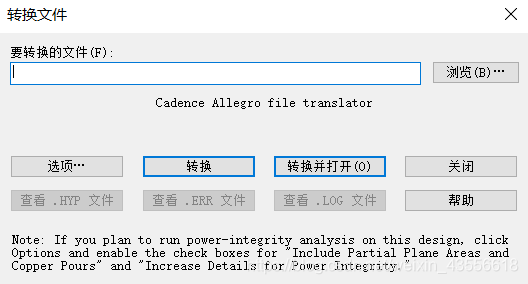
How to convert .brd to .hyp file?You can try to use HyperLynx’s built-in conversion function to directly convert Allegro’s .brd file, but this method may encounter some problems and cause the conversion to fail.
If the built-in conversion function fails, you can try to convert the .brd file to ODB++ format and then import it into HyperLynx. The specific steps are as follows:
Open the PCB file in Allegro, select “File” -> “Export”, and then select ODB++ format for export.
After the export is successful, open HyperLynx, select “File” -> “Open ODB++”, select the exported ODB file, and wait for the import to complete before performing PCB board-level simulation. 1. If the above method still cannot solve the problem, you can try to add the system variable CDSROOT to solve the conversion failure problem. The specific steps are as follows:
Add the system variable CDSROOT, and the value is the installation path of Cadence Allegro, such as D:\Cadence\Cadence_SPB_17.2-2016\tools\bin.
After confirming, restart the computer and try the conversion operation again
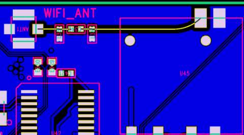
How to convert Cadence17.2’s .brd file to HyperLynx9.4.1’s .hyp file
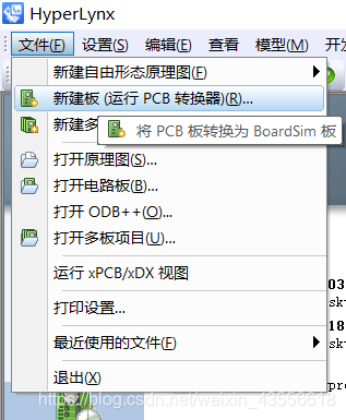
How to convert Cadence17.2’s .brd file to HyperLynx9.4.1’s .hyp file?Recently, I used Hyperlynx to simulate the signal integrity of PCBs, and I needed to convert various PCB formats into .hyp formats. In the process, I found that the PCB drawn by AD can be directly exported in .hyp format, which is very convenient, but the PCB drawn by Cadence cannot be directly exported. I need to use the built-in PCB converter of Hyperlynx to convert the .brd file of Cadence, as shown below:
But the conversion has always failed. I checked the .ERR file and found a line like this: ERROR: Cadance Allegro utility:extracta, so it is a problem with extracta.exe.
The specific solution is to add the system variable CDSROOT, and the value is D:\Cadence\Cadence_SPB_17.2-2016\tools\bin (the location of your extracta.exe). After confirming, restart the computer and the problem is solved.
Tutorial on converting Cadence17.2’s .brd file to HyperLynx9.4.1’s .hyp file
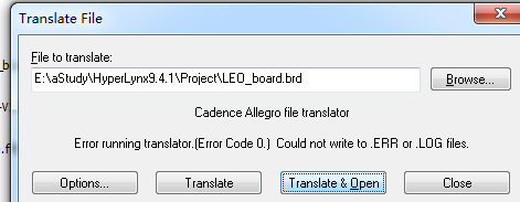
HyperLynx’s built-in conversion function can directly convert Allegro’s .brd file for use, but for some reason the following error always occurs. I didn’t find a solution online, so I had to find another way.
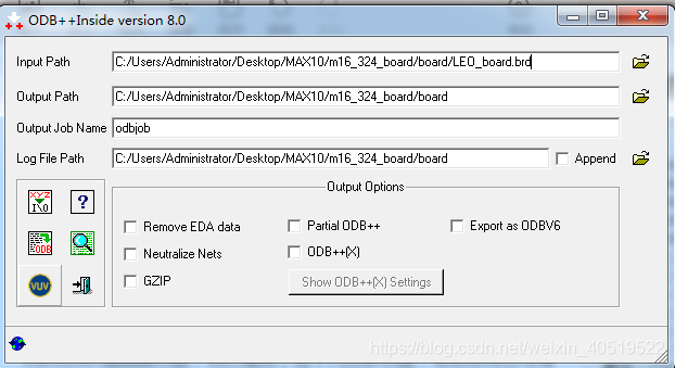
Another way to import PCB into HyperLynx is to convert the file to ODB++inside format. This method requires the installation of the ODB++inside plug-in in advance.
After installing the plug-in, you can convert the .brd file.
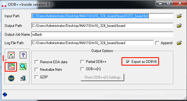
First open the PCB file in Allegro, select ODB++inside in file–>export, the following figure appears, select Export as ODBV6, click 1, and then click Accept.
Wait for the conversion to succeed.
This file is the converted file
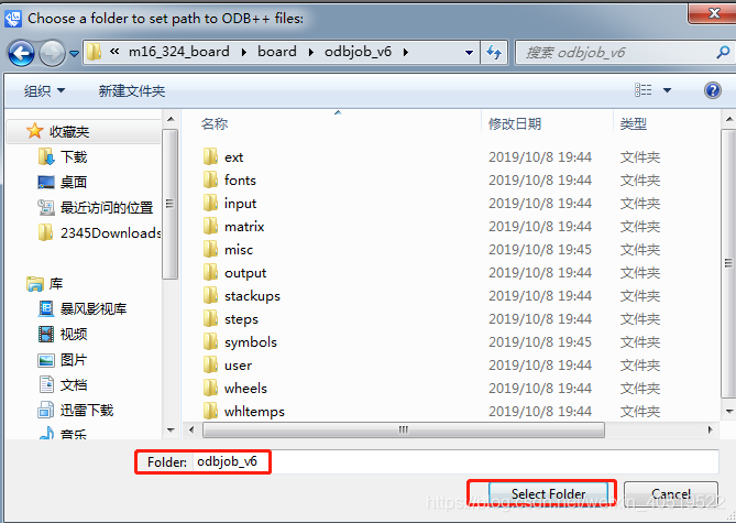
Open HyperLynx9.4.1, select open ODB++ in file, select the odbjob_v6 folder, and click select folder.
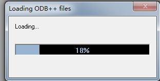
Wait to open.
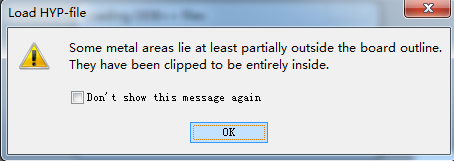
Click ok. .
What is a .hyp file?
.hyp file is a file used to record key information such as boundary conditions, material properties, solver settings, etc. of the analysis. This file is usually associated with HyperWorks analysis software and is the basis for numerical calculation and analysis.
The specific uses of .hyp files include:
Geometry model file: represents the geometry of the product or structure. Mesh file: shows the process of dividing the model into finite elements. Simulation setting file: records the key setting information of the analysis. Result file: contains the calculated engineering quantities such as strain, stress, displacement, etc. Post-processing file: used to visualize and analyze results in tools such as HyperView. Report document: usually in PDF or Word format, recording detailed results and conclusions of the analysis1. In terms of use, for example, in PCB tool software, .hyp files can be created and edited through the BroadSim function, including setting line characteristics, editing stacking information, etc., to simulate and analyze circuit boards2. In addition, the Hype software also supports exporting to .hyp format files for further analysis and processing.
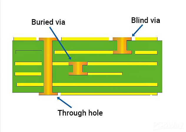
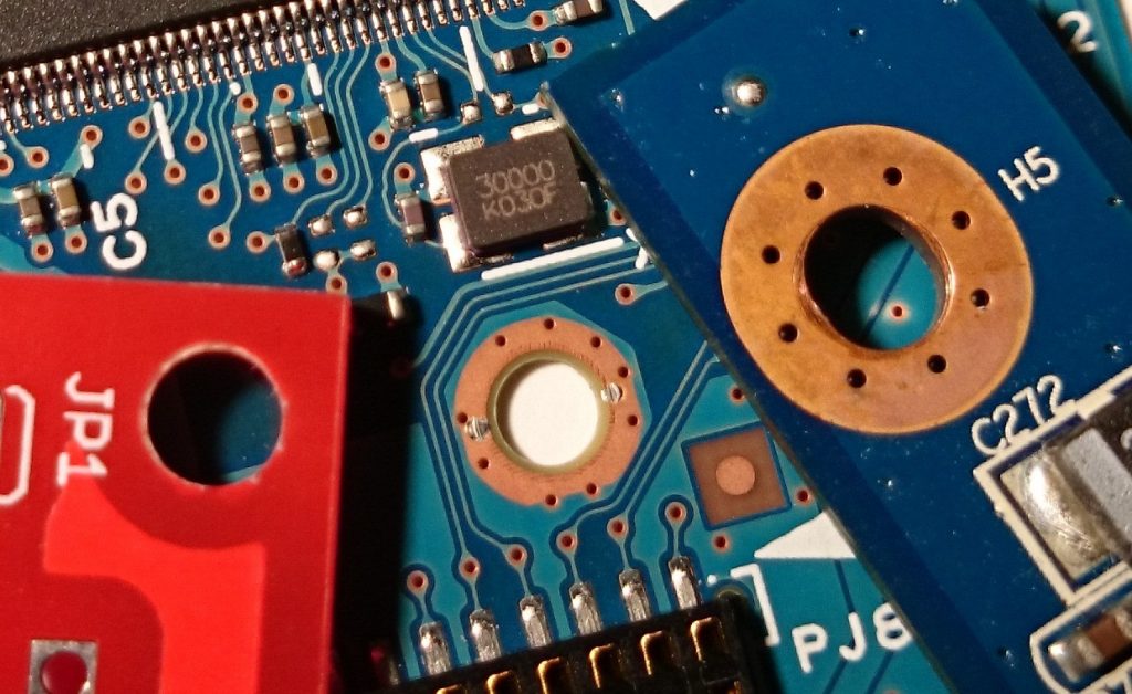
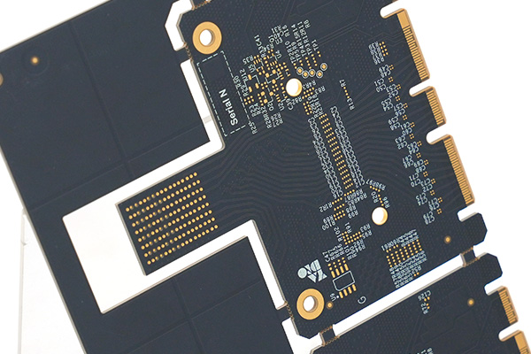
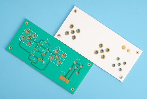
Board electronics with holes The types of vias in PCB include through holes, blind holes and buried holes, which have different characteristics and requirements in design and manufacturing. The selection of the appropriate via type should consider the number of PCB layers, wiring density, signal frequency, cost budget and production process. The via design should pay attention to avoid affecting the welding quality, preventing electrical short circuits, and saving costs in high-density packaging.
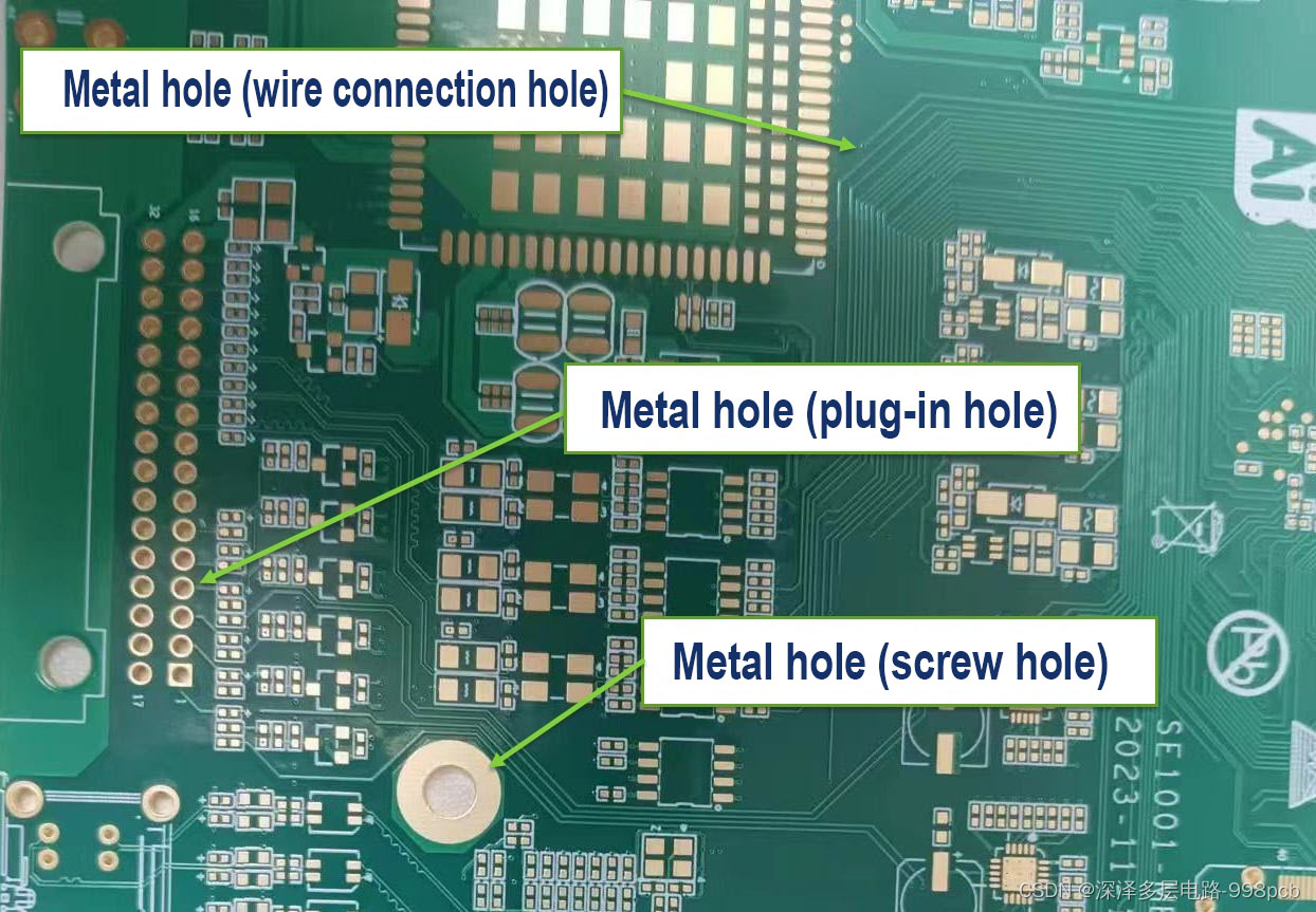
What are the holes in a PCB called?
What are the holes on PCB called? What are the holes in the circuit? The holes on PCB can be roughly divided into 3 types, screw holes (mounting holes), conductive holes (vias), and plug-in holes.
Screw holes: Screw holes are used for fixing.
Conductive holes: Conductive holes (also called vias) are used for conducting electricity just like circuits.
Plug-in holes: Plug-in holes are of course used to plug in various parts, such as diodes, transistors, capacitors, inductors, etc.
What is a through hole
What is a through hole? Through holes, also known as perforations, are holes in a PCB that go all the way through the board. Their main purpose is to provide electrical connections for component pins while allowing soldering on both sides of the board.
1.A via is a special through hole whose wall is metallized to achieve electrical connection between different layers on a circuit board. This type of hole is usually used to connect component pins to internal circuits, or to achieve electrical connection between different layers in a multi-layer PCB. Vias need to be metallized during the PCB manufacturing process, which usually includes drilling, desmearing, chemical copper plating, and electroplating.
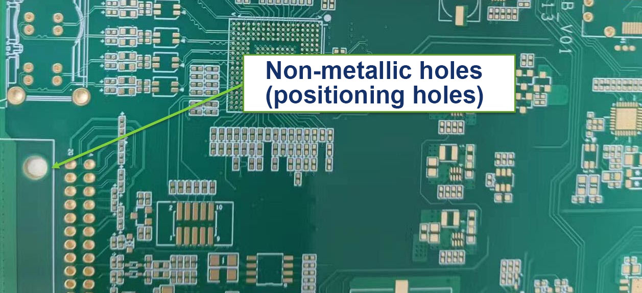
2.Non-conducting holes are the opposite of through holes. Their hole walls are not metallized, so they do not have electrical connection functions. These holes are mainly used for mechanical fixation, heat dissipation or identification purposes. Non-conducting holes are relatively simple in the PCB manufacturing process, and only drilling operations are required.
What is a blind via?
A blind via is a hole that extends from one side of a PCB to a certain internal layer without penetrating the entire board. The emergence of blind vias is mainly due to the development of HDI technology, which provides circuit designers with greater flexibility and more compact layout. Blind vias are usually used to connect surface mount components (SMD) to internal circuit layers, or to connect circuits between different internal layers.
What are buried vias?
Buried vias are holes located inside the PCB that do not penetrate any side of the board. They are completely hidden inside the board and are used to connect circuits between different internal layers. Buried vias are especially useful in HDI boards because they can reduce the overall thickness of the board while maintaining electrical connections between internal circuits.
What is a microvia?
Microvia refers to a hole with a smaller diameter, usually at the micron level. The emergence of microvia technology enables PCB designers to achieve more complex circuit layouts in a smaller space. Microvias are often used in high-density, high-reliability electronic devices such as mobile phones and tablets. The manufacture of microvias requires high-precision drilling equipment and technology to ensure the accuracy and reliability of the holes.
What are Mounting holes?
What are Mounting holes?Locking holes are auxiliary holes used in the PCB manufacturing and assembly process to accurately locate and fix the circuit board. They are usually located at the edge or specific position of the PCB to ensure that the circuit board can be accurately aligned and fixed during manufacturing, testing and assembly. The locating holes do not participate in the connection of the circuit, but are essential to ensure the quality and performance of the circuit board.
What are Mounting holes?
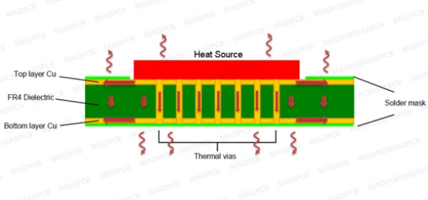
What are thermal vias?
Thermal vias are holes designed specifically for heat dissipation, usually large and can run through the entire PCB or multiple layers. Their role is to reduce heat buildup on the circuit board by increasing surface area and air flow, thereby improving the stability and reliability of the device. Thermal vias are particularly important in high-performance, high-power electronic devices.
FAQ About board electronics with holes
How to solve the contradiction between manual routing and automatic routing of high-speed signals?
Most of the current powerful routing software’s automatic routing tools have set constraints to control the routing method and the number of vias. The routing engine capabilities and constraint setting items of various EDA companies are sometimes very different. For example, whether there are enough constraints to control the winding method of the serpentine, whether the routing spacing of the differential pair can be controlled, etc. This will affect whether the routing method generated by automatic routing can meet the designer’s ideas. In addition, the difficulty of manually adjusting the routing is also related to the capabilities of the routing engine. For example, the pushing ability of the routing, the pushing ability of the via, and even the pushing ability of the routing pair copper. Therefore, choosing a routing tool with strong routing engine capabilities is the solution.
Will adding test points affect the quality of high-speed signals?
As for whether it will affect the signal quality, it depends on the method of adding test points and how fast the signal is. Basically, the additional test points (not using the existing vias (via or DIP pins) as test points) may be added to the line or a small section of wire may be pulled out from the line. The former is equivalent to adding a very small capacitor to the line, while the latter is an additional branch. Both of these situations will have some impact on high-speed signals, and the extent of the impact is related to the frequency speed of the signal and the edge rate of the signal. The magnitude of the impact can be learned through simulation. In principle, the smaller the test point, the better (of course, it must meet the requirements of the test equipment) and the shorter the branch, the better.
Can you introduce some foreign technical books and data on high-speed PCB design?
Now the application of high-speed digital circuits includes communication networks and calculators and other related fields. In the communication network, the operating frequency of PCB boards has reached around GHz, and the number of layers is as many as 40 layers as far as I know. Due to the advancement of chips, the operating frequency of calculator-related applications, whether it is a general PC or server, has reached 400MHz (such as Rambus) or above. In response to the demand for high-speed and high-density routing, the demand for blind/buried vias, mircrovias and build-up process technology is gradually increasing. These design requirements can be mass-produced by manufacturers.
Does the design of rigid-flexible boards require special design software and specifications? Where can I undertake the processing of such circuit boards in China?
Can I use general PCB design software to design flexible printed circuits (Flexible Printed Circuit). The Gerber format is also used for FPC manufacturers to produce. Since the manufacturing process is different from that of general PCBs, each manufacturer will have its own restrictions on line width, line spacing, and aperture (via) based on their manufacturing capabilities. In addition, some copper foil can be laid at the turning point of the flexible circuit board for reinforcement. As for the manufacturer, you can search for “FPC” as a keyword on the Internet and you should be able to find it.
If the size of the circuit board is fixed, if the design needs to accommodate more functions, it is often necessary to increase the routing density of the PCB, but this may lead to increased mutual interference between the routings, and at the same time, the impedance cannot be reduced if the routing is too thin. Please introduce the techniques in the design of high-speed (>100MHz) high-density PCBs?
When designing high-speed and high-density PCBs, crosstalk interference does need to be paid special attention to because it has a great impact on timing and signal integrity. Here are a few things to note:
Control the continuity and matching of the characteristic impedance of the trace.
The size of the trace spacing. The spacing commonly seen is twice the line width. Through simulation, you can know the impact of trace spacing on timing and signal integrity and find the tolerable spacing. The results of different chip signals may be different.
Choose an appropriate termination method.
Avoid the same routing direction of the upper and lower adjacent layers, or even have traces overlapped up and down, because this kind of crosstalk is greater than the case of adjacent traces on the same layer.
Use blind/buried vias to increase the trace area. However, the production cost of the PCB board will increase. It is indeed difficult to achieve complete parallelism and equal length in actual implementation, but it should be done as much as possible.
In addition, differential termination and common mode termination can be reserved to mitigate the impact on timing and signal integrity.
The RF part, IF part, and even the low-frequency circuit part of the outdoor unit are often deployed on the same PCB. What are the material requirements for such PCB? How to prevent interference between RF, IF, and even low-frequency circuits?
Hybrid circuit design is a big problem. It is difficult to have a perfect solution.
Generally, RF circuits are laid out and wired as an independent single board in the system, and there will even be a special shielding cavity. Moreover, RF circuits are generally single-sided or double-sided boards, and the circuits are relatively simple. All of these are to reduce the impact on the distributed parameters of RF circuits and improve the consistency of RF systems. Compared with general FR4 materials, RF circuit boards tend to use high-Q substrates. The dielectric constant of this material is relatively small, the distributed capacitance of the transmission line is small, the impedance is high, and the signal transmission delay is small. In hybrid circuit design, although RF and digital circuits are made on the same PCB, they are generally divided into RF circuit area and digital circuit area, and laid out and wired separately. Shielding is used between ground vias and shielding boxes.
Best is mainly engaged in the production of High frequency pcb communication circuits, high-speed, microwave and radio frequency printed circuit boards, mainly in sample making and small and medium batches. The main products are: microwave radio frequency high-frequency boards, Rogers high-frequency boards, Rogers multi-layer high-frequency mixed-pressure boards, Rogers radio frequency boards, Taconic microwave boards, Taconic multi-layer circuit boards, Arlon microstrip antenna boards, ARLON high-frequency boards, F4BM antenna boards, F4BM multi-layer mixed-pressure boards, radio frequency amplifier PCB boards, HDI precision multi-layer boards, serving domestic and foreign high-tech enterprises and scientific research institutions.
What is a high frequency pcb communication circuits
High frequency pcb communication circuits to a circuit board with an operating frequency in the high frequency band (usually greater than 300MHz or a wavelength less than 1 meter), which is mainly used to transmit high-frequency signals and data. This type of circuit board is widely used in radio frequency (RF) and microwave fields, such as communication equipment, radar systems, satellite communications, and high-speed data transmission systems.
What is a high frequency pcb communication circuits
The characteristics of high-frequency circuits include challenges such as transmission line effects, signal integrity issues, and electromagnetic interference (EMI). Due to the short wavelength of high-frequency signals, traditional low-frequency circuit design methods are no longer applicable, and special design and processing methods are required to ensure the performance and stability of the circuit.
High-frequency circuit boards are produced on microwave substrate copper-clad boards using ordinary rigid circuit board manufacturing methods or special processing methods. They need to have high-quality electrical properties and chemical stability to meet the requirements of high-frequency signal transmission.
Definition of high frequency pcb communication circuits
High-frequency circuit board, as a special circuit board, is mainly suitable for occasions with high electromagnetic frequency, especially in the fields of high frequency (frequency greater than 300MHz or wavelength less than 1 meter) and microwave (frequency greater than 3GHz or wavelength less than 0.1 meter).
It is a circuit board made on a microwave substrate copper-clad board by adopting some manufacturing processes or special processing methods of ordinary rigid circuit boards. Generally speaking, when the frequency of the circuit board reaches above 1GHz, it can be defined as a high-frequency board.
With the rapid development of science and technology, more and more equipment designs have begun to involve microwave frequency bands (>1GHz) and even expanded to the millimeter wave field (such as 77GHz), especially in popular applications such as 77GHz millimeter wave antennas on vehicles.
This trend not only promotes the continuous increase in frequency, but also puts higher requirements on the substrate of the circuit board.
For example, the substrate material needs to have excellent electrical properties, stable chemical properties, and as the frequency of the power signal increases, the loss on the substrate must be extremely small. Therefore, the importance of high-frequency boards is becoming more and more prominent.
Advantages of high frequency pcb communication circuits
The main advantages of high frequency pcb communication circuits include efficient data transmission, strong anti-interference ability, high-frequency bandwidth and high reliability.
high frequency pcb communication circuits can achieve efficient data transmission. High-frequency signals have a short cycle and can transmit more information per unit time, so they have the advantage of large-capacity transmission. In addition, high-frequency signals can achieve fast signal processing and are suitable for application scenarios that require high-speed data transmission and high real-time requirements.
high frequency pcb communication circuits have strong anti-interference capabilities. Due to the short wavelength of high-frequency signals, they can better avoid external interference and attenuation and have strong anti-interference capabilities. This makes high-frequency signals have advantages in fields such as wireless communications and radar systems, and can achieve stable signal transmission and reception.
high frequency pcb communication circuits also have the advantage of high-frequency bandwidth. High-frequency signals correspond to a larger frequency range and can provide higher bandwidth than low-frequency signals. This means that more data can be transmitted, thereby supporting higher data rates and richer media content.
High reliability of high frequency pcb communication circuits is also one of its advantages. The use of high-quality materials and manufacturing processes can effectively resist external interference and oxidation corrosion, ensure stable performance in high temperature environments, and thus extend the service life of the circuit board.
Classification of high frequency pcb communication circuits
Classification by material:
Organic materials: including phenolic resin, glass fiber/epoxy resin, Polyimide, BT/Epoxy (bismaleimide triazine/epoxy resin), etc.
Inorganic materials: mainly including aluminum, copper-invar-copper, ceramic, etc. These materials are mainly selected for their excellent heat dissipation function.
Classification by the hardness of the finished product:
Rigid PCB: has a solid structure and stable performance.
Flexible PCB: has flexibility and bendability, suitable for occasions requiring flexible wiring.
Rigid-Flex PCB: It combines the characteristics of rigid and flexible boards, and has higher design flexibility and wide application.
Classification by structure:
Single-sided board: A circuit board with a conductive layer on only one side.
Double-sided board: Both sides are coated with conductive layers, separated by insulating materials in the middle.
Multilayer board: It is composed of multiple conductive layers and insulating layers, and has higher circuit integration and reliability.
Classification by use:
Communication board: It is used in various communication equipment and systems.
Consumable electronic board: It is commonly found in consumer electronic products.
Military board: A circuit board that meets special requirements in the military field.
Computer board: A circuit board used in computer hardware.
Semiconductor board: A circuit board used in the manufacturing and testing process of semiconductors.
Electrical test board: A circuit board used in electronic testing and measurement equipment.
How to choose high-frequency circuit board high-speed board
When choosing PCB board, you must find a balance between meeting design requirements, mass production and cost. In short, the design requirements cover two aspects: electrical performance and structural reliability. Especially when designing ultra-high-speed PCB (frequency greater than GHz), the choice of board is particularly important. For example, the commonly used FR-4 material will have a significantly increased dielectric loss (Df, i.e., Dielectric Loss) at a frequency of several GHz, and may no longer be applicable.
Taking the 10Gb/S high-speed digital signal as an example, this signal can be regarded as the superposition of multiple sinusoidal wave signals of different frequencies. Therefore, the 10Gb/S signal contains multiple components of different frequencies: such as a 5GHz fundamental signal, a 3rd-order 15GHz signal, a 5th-order 25GHz signal, and a 7th-order 35GHz signal. In order to ensure the integrity of digital signals, maintain the steepness of the upper and lower edges of the signals, and be compatible with the low-loss, low-distortion transmission of RF microwaves (the high-frequency harmonic part of the digital signal reaches the microwave frequency band), the selection of materials for high-speed digital circuit PCBs has many similarities with the needs of RF microwave circuits.
In actual engineering operations, the selection of high-frequency boards seems simple, but the factors that need to be considered are quite complex. Through the introduction of this article, PCB design engineers or high-speed project leaders can have a deeper understanding of the characteristics and selection of boards. Understand the electrical properties, thermal properties, reliability and other characteristics of the board, and use the stacking design reasonably to create products with high reliability and excellent processability, and achieve the best balance of various factors.
Composition and key components of high frequency pcb communication circuits
High frequency pcb communication circuits are basically composed of passive components, active devices and passive networks. Passive components include resistors, capacitors and inductors, which mainly exhibit resistance characteristics at low frequencies, but also exhibit reactance characteristics at high frequencies. Active devices such as high-frequency triodes have the characteristics of high gain, high frequency response and low noise, and are widely used in television, radio communication, radar and other fields.
Application of high frequency pcb communication circuits
High frequency pcb communication circuits are widely used in long-distance communication systems, with a communication distance of up to thousands of kilometers, and are often used to maintain communication between aircraft and bases. It occupies a high-frequency band of 2~30MHz, uses skywave propagation, and can propagate over long distances. Modern airborne high-frequency communication systems usually use single-sideband communication systems, which can greatly compress the occupied frequency band and save transmission power. However, high-frequency communication is also susceptible to electrical interference such as ionospheric disturbances and lightning, generating radio background noise, and there is fading, and the signal is sometimes strong and sometimes weak.
Design Guidelines for High Frequency PCB Communication Circuits
Design Guidelines
High Frequency PCB Communication Circuits
How to avoid high-frequency interference?
The basic idea of avoiding high-frequency interference is to minimize the interference of the electromagnetic field of high-frequency signals, which is the so-called crosstalk. You can increase the distance between high-speed signals and analog signals, or add ground guard/shunt traces next to analog signals. Also pay attention to the noise interference of digital ground to analog ground.
How to solve the signal integrity problem in high-frequency communication PCB design?
Signal integrity is basically an impedance matching problem. The factors that affect impedance matching include the architecture and output impedance of the signal source, the characteristic impedance of the trace, the characteristics of the load end, and the topology of the trace. The solution is to rely on termination and adjust the topology of the trace.
How is the differential wiring method implemented?
There are two points to note when wiring differential pairs. One is that the length of the two lines should be as equal as possible, and the other is that the spacing between the two lines (this spacing is determined by the differential impedance) should remain unchanged, that is, they should be kept parallel. There are two parallel methods, one is that two lines run on the same routing layer (side-by-side), and the other is that two lines run on two adjacent layers (over-under). Generally, the former side-by-side (side by side, shoulder to shoulder) is more commonly used.
How to implement differential routing for clock signal lines with only one output end?
To use differential routing, it must be meaningful if both the signal source and the receiving end are differential signals. Therefore, differential routing cannot be used for clock signals with only one output end.
Can a matching resistor be added between the differential line pairs at the receiving end?
The matching resistor between the differential line pairs at the receiving end is usually added, and its value should be equal to the value of the differential impedance. This will improve the signal quality.
Why should the routing of differential pairs be close and parallel?
The routing method of differential pairs should be appropriately close and parallel. The so-called appropriate proximity is because this spacing will affect the value of differential impedance, which is an important parameter for designing differential pairs. Parallelism is also required because the consistency of differential impedance must be maintained. If the two lines are sometimes far away and sometimes close, the differential impedance will be inconsistent, which will affect the signal integrity and timing delay.
How to deal with some theoretical conflicts in actual wiring?
Basically, it is right to separate the analog/digital ground. It should be noted that the signal routing should try not to cross the split place (moat), and the return current path of the power supply and signal should not be too large.
The crystal oscillator is an analog positive feedback oscillation circuit. To have a stable oscillation signal, the loop gain and phase specifications must be met. The oscillation specification of this analog signal is easily interfered. Even if ground guard traces are added, it may not be possible to completely isolate the interference. Moreover, if it is too far away, the noise on the ground plane will also affect the positive feedback oscillation circuit. Therefore, the distance between the crystal oscillator and the chip must be as close as possible.
It is true that there are many conflicts between high-speed wiring and EMI requirements. But the basic principle is that the resistors, capacitors or ferrite beads added due to EMI cannot cause some electrical characteristics of the signal to not meet the specifications. Therefore, first use the techniques of arranging routing and PCB stacking to solve or reduce EMI problems, such as routing high-speed signals on the inner layer. Only then use resistors, capacitors or ferrite beads to reduce damage to the signal.
How to solve the contradiction between manual routing and automatic routing of high-speed signals?
Most of the current powerful routing software’s automatic routing tools have set constraints to control the winding method and the number of vias. The winding engine capabilities and constraint setting items of various EDA companies are sometimes very different. For example, whether there are enough constraints to control the winding method of the serpentine, whether the routing spacing of the differential pair can be controlled, etc. This will affect whether the routing method generated by automatic routing can meet the designer’s ideas. In addition, the difficulty of manually adjusting the routing is also related to the ability of the winding engine. For example, the pushing ability of the routing, the pushing ability of the via, and even the pushing ability of the routing to the copper plating, etc. Therefore, choosing a routing tool with a strong winding engine capability is the solution.
About test coupon.
The test coupon is used to measure the characteristic impedance of the produced PCB board with TDR (Time Domain Reflectometer) to see if it meets the design requirements. Generally, the impedance to be controlled is single line and differential pair. Therefore, the trace width and line spacing (when there is a differential pair) on the test coupon should be the same as the line to be controlled. The location of the ground point during measurement is important. In order to reduce the inductance of the ground lead, the grounding point of the TDR probe is usually very close to the probe tip, so the distance and method between the point where the signal is measured on the test coupon and the ground point should be consistent with the probe used.
In high-speed PCB design, the blank area of the signal layer can be copper-plated, and how should the copper of multiple signal layers be distributed in grounding and power supply?
Generally, the copper plating in the blank area is mostly grounded. However, when plating copper next to high-speed signal lines, pay attention to the distance between the copper plating and the signal line, because the copper plating will reduce the characteristic impedance of the trace a little. Also be careful not to affect the characteristic impedance of other layers, such as in the dual strip line structure.
Can the signal line on the power plane be calculated using the microstrip line model? Can the signal between the power and ground planes be calculated using the stripline model?
Yes, both the power plane and the ground plane must be considered as reference planes when calculating the characteristic impedance. For example, a four-layer board: top layer-power layer-ground layer-bottom layer. At this time, the model of the characteristic impedance of the top layer routing is a microstrip line model with the power plane as the reference plane.
Can the automatic generation of test points on high-density printed circuit boards by software generally meet the test requirements of mass production?
Whether the test points automatically generated by general software meet the test requirements depends on whether the specifications for adding test points meet the requirements of the test equipment. In addition, if the routing is too dense and the specifications for adding test points are strict, it may not be possible to automatically add test points to each line. Of course, the places to be tested need to be filled manually.
Will adding test points affect the quality of high-speed signals?
As for whether it will affect the signal quality, it depends on the way of adding test points and how fast the signal is. Basically, the additional test point (without using the existing via or DIP pin as the test point) may be added to the line or a short line may be pulled out from the line. The former is equivalent to adding a very small capacitor to the line, and the latter is an additional branch. Both situations will have some impact on the high-speed signal, and the degree of impact is related to the frequency speed of the signal and the edge rate of the signal. The magnitude of the impact can be known through simulation. In principle, the smaller the test point, the better (of course, it must meet the requirements of the test equipment) and the shorter the branch, the better.
How should the ground wires between the boards of a system be connected when several PCBs are connected to each other?
When the signals or power supplies between the PCB boards are in operation, for example, when the power supply or signal from board A is sent to board B, there will be an equal amount of current flowing back from the ground layer to board A (this is Kirchoff current law). The current on the ground layer will flow back to the impedance. Therefore, at each interface where the power supply or signal is connected to each other, the number of pins allocated to the ground layer should not be too small to reduce the impedance, so as to reduce the noise on the ground layer. In addition, the entire current loop can be analyzed, especially the part with larger current, and the connection method of the ground layer or ground wire can be adjusted to control the flow of current (for example, create low impedance at a certain place to let most of the current flow through this place) to reduce the impact on other more sensitive signals.
What is an alumina circuit board? As a unique circuit board material, it is emerging in the electronics field with its excellent performance and advantages. It uses alumina as the main material, bringing new opportunities for performance improvement and miniaturization of various electronic devices.
What is an alumina circuit board?
Alumina circuit board is a circuit board that uses alumina ceramic as a substrate. This circuit board has excellent electrical insulation properties, high thermal conductivity, excellent soft solderability and high adhesion strength. It can be etched with various graphics like a PCB board and has a large current carrying capacity.
Alumina ceramic circuit board is an ultra-thin composite substrate made by bonding copper foil directly to the surface (single or double sides) of an alumina (Al2O3) ceramic substrate at high temperature through a special process.
Alumina ceramic circuit boards are widely used in electronic devices that require high performance and high reliability, such as solar applications, voltage regulators, amplifier circuits, and memory modules.
Alumina ceramic substrates are mainly composed of white amorphous powder, commonly known as alumina or simply Al2O3. It has excellent properties, such as high wear resistance, acid and alkali corrosion resistance, excellent performance at high temperatures (1600-1700 degrees Celsius), etc.
What types of alumina circuit boards are there?
Ordinary alumina ceramics are classified according to their Al2O3 content, including 99%, 96%, etc. 99% alumina has high purity, white or ivory color, and is widely used in various applications, including lamps, electronic devices, and wear-resistant components. 96% alumina is widely used in various electronic applications while providing good thermal conductivity and insulation properties.
96% alumina:
Suitable for thick film circuit substrates, with excellent electrical insulation properties, mechanical strength, good thermal conductivity, chemical durability and dimensional stability.
Its surface roughness is generally 0.2~0.6μm, and the maximum operating temperature of the substrate can reach 1600℃.
96% alumina has become an economical choice for manufacturing hybrid microelectronic circuits due to its availability, low cost and technical quality.
99% Alumina:
Commonly used for most thin-film electronic substrate applications such as sputtering, evaporation, and chemical vapor deposition of metals for circuit generation.
99% Alumina has higher purity, smaller grain size, and the prepared substrate has excellent surface smoothness (surface roughness is generally 0.08~0.1μm), and the maximum use temperature of the substrate can reach 1700℃.
It has high mechanical strength, low thermal conductivity, excellent electrical insulation, good dielectric properties, and good corrosion resistance and wear resistance.
What are the advantages of alumina circuit boards?
The advantages of alumina circuit boards are mainly reflected in their physical and chemical properties, which make them widely used in many fields.
High hardness: The hardness of alumina ceramic plates is very high, second only to diamond and sapphire, and has excellent wear resistance and corrosion resistance.
High melting point: The melting point of alumina is as high as 2072℃, which means that alumina circuit boards can work for a long time in high temperature environments without being affected and maintain stable performance.
Good insulation performance: Alumina ceramic boards have good insulation performance and can effectively isolate the conduction of current and heat.
Excellent heat dissipation performance: In LED lighting and high-power electronic devices, alumina circuit boards are widely used due to their excellent heat dissipation performance.
Lightweight: Compared with other materials, alumina ceramic boards have a lower density and lighter weight, which can greatly reduce the load of the equipment.
Chemical stability: Alumina is an electrical insulating material with high resistivity, good chemical stability and good corrosion resistance.
What are the disadvantages of alumina circuit boards?
The disadvantages of alumina ceramic PCBs mainly include high cost, fragility, inferior thermal conductivity to other materials, complex manufacturing process and high price.
High cost: Compared with plastic packaging, alumina ceramic PCBs have higher process temperature requirements, which leads to relatively high costs.
Fragile: Alumina ceramics are relatively fragile, and compared with aluminum nitride ceramic substrates, alumina ceramics are more fragile.
Thermal conductivity is not as good as other materials: Although alumina ceramics have certain thermal conductivity, their thermal conductivity is usually between 25W and 50W, while the thermal conductivity of aluminum nitride ceramic substrates can reach 190~260W. In comparison, the thermal conductivity of alumina ceramics is poor.
Complicated manufacturing process: Due to the high hardness of alumina ceramics, mechanical processing is more difficult, which increases the cost of its precision machined parts.
Higher price: Due to the above factors, the price of alumina ceramic PCBs is usually higher, about 3~10 times that of resin PCB boards.
What are the uses of alumina circuit boards?
Alumina circuit boards are widely used and are mainly used in the following aspects:
Electronic industry: Alumina ceramic circuit boards have become the preferred material in the manufacture of electronic components such as semiconductor devices and integrated circuits due to their excellent insulation properties and high temperature resistance.
Optoelectronic industry: In the field of optoelectronics, alumina ceramic circuit boards also perform well. Due to their high optical transparency and chemical stability, they are widely used in the manufacture of optoelectronic devices such as lasers and LEDs.
Automobile Industry: In terms of automobile headlights, the popularity of high-power LED headlights has put forward higher requirements for heat dissipation performance. Alumina ceramic substrates, with their good thermal conductivity, ensure the stable operation of LED light sources and improve lighting effects and service life.
Aerospace: Alumina ceramic substrates have been widely used in key components such as aerospace devices and satellite communication equipment due to their comprehensive performance advantages.
Medical Devices: Due to their excellent physical, chemical and mechanical properties, alumina ceramic circuit boards can meet the high requirements of medical devices for materials and ensure the performance and safety of medical devices.
In summary, alumina circuit boards have been widely used in many fields due to their unique physical, chemical and mechanical properties, providing solid support for technological progress and industrial upgrading in all walks of life.
Is alumina a good electrical insulator?
Alumina PCB is a good electrical insulator.
Alumina (Al₂O₃), as a common ceramic material, has good electrical insulation, high temperature resistance and mechanical strength. Its color is usually white or light yellow, its volume density is between 3.7-3.9 g/cm³, its thermal conductivity is as high as 24 W/(m·K) or more, and its bending strength is usually between 300-400 MPa.
In addition, alumina also has a low dielectric constant and breakdown voltage, which makes it particularly suitable for high-frequency circuits and high-voltage circuits.
Therefore, alumina PCB is not only one of the most commonly used ceramic PCBs on the market because of its low price and excellent performance, but also when using alumina PCB, there is no need to add an insulating layer, which further proves its good electrical insulation.
What other ceramic PCB materials are there?
In addition to alumina ceramic PCB materials, it also includes alumina, aluminum nitride, silicon carbide, silicon nitride, zirconium oxide, etc. These materials each have unique properties and are suitable for different application scenarios.
Aluminum nitride (AlN): Aluminum nitride is also an excellent ceramic material with extremely high thermal conductivity and low expansion coefficient. It is gray in color and has a volume density between 3.33-3.35 g/cm³. The thermal conductivity of aluminum nitride is as high as 170 W/(m·K), which is several times that of traditional organic materials. The flexural strength can reach about 400-500 MPa, and it also has a low dielectric constant, which is suitable for high-power electronic devices and high-speed digital circuits.
Silicon Carbide (SiC): Silicon carbide is a hard material with excellent wear resistance and corrosion resistance. It is gray in color and has a volume density of 3.1-3.15 g/cm³. Silicon carbide has a high thermal conductivity of up to 100 W/(m·K), a flexural strength of more than 450 MPa, and a low dielectric constant and breakdown voltage, which is suitable for power electronic devices in high temperature environments.
Silicon Nitride (Si3N4): Silicon nitride is a high-strength, high-toughness ceramic material widely used in the aerospace field. It is gray in color and has a volume density of about 3.22 g/cm³. Silicon nitride has a high thermal conductivity of up to 20 W/(m·K), a flexural strength of generally between 700-1200 MPa, and a low dielectric constant and breakdown voltage, which makes it suitable for electronic components in high temperature and high pressure environments.
Zirconium oxide (ZrO2): Zirconium oxide is a high-toughness, high-hardness ceramic material with good chemical stability. It is gray in color and has a volume density of about 6.0 g/cm³. Zirconium oxide has a high thermal conductivity of up to 3 W/(m·K), a flexural strength of about 100-400 MPa, and a low dielectric constant and breakdown voltage, which makes it suitable for electronic components in high temperature and high pressure environments.
In short, alumina ceramic PCBs are increasingly used in the electronic field. It not only provides a solid foundation for the innovative development of electronic equipment, but also opens up a new path for the advancement of future electronic technology. BEST Technology is a professional ceramic circuit board manufacturer with rich manufacturing experience in various ceramic materials, and its product quality has passed relevant quality inspections. Choosing us will get the best quality products!
In the field of electronics, ceramic circuit boards are quietly opening a new revolution with their unique charm and excellent performance. Ceramic circuit boards are gradually becoming the focus of the electronics industry, leading the industry to a more efficient, stable and advanced technological era.
What is a ceramic pcb board?
ceramic pcb board, also known as ceramic printed circuit board, is a printed circuit board that uses ceramic as a substrate instead of traditional fiberglass or epoxy resin. Compared with traditional substrates, ceramic materials have a variety of advantages, making them ideal for high-performance electronic applications.
What are the different types of ceramic PCB?
There are several types of ceramic materials commonly used in PCB boards, including aluminum oxide (Al₂O₃), aluminum nitride (AlN), and beryllium oxide (BeO). Each material has its own unique properties and advantages.
1. Alumina ceramic pcb board
Alumina is the most widely used ceramic material in PCB boards. It has excellent electrical insulation, high thermal conductivity and good mechanical strength. Alumina ceramic pcb boards are suitable for a wide range of applications, including power electronics, LED lighting and automotive electronics.
2. Aluminum Nitride ceramic pcb board
Aluminum nitride is a high-performance ceramic material with extremely high thermal conductivity. This makes it ideal for applications where heat dissipation is a key factor, such as high-power LEDs, power modules, and RF/microwave equipment.
3. Beryllium Oxide ceramic pcb board
Beryllium oxide is a highly toxic material, but it has excellent thermal conductivity and electrical insulation. Due to its toxicity, beryllium oxide ceramic pcb boards are only used in special applications where other materials cannot meet the performance requirements.
What is the high temperature ceramic PCB?
High temperature ceramic PCB is a special ceramic circuit board designed for high temperature environments, commonly known as high temperature co-fired ceramic (HTCC) circuits. This circuit board is made by mixing adhesives, lubricants, solvents, plasticizers, and aluminum oxide to make raw ceramics, and then forming circuits.
The main feature of high temperature ceramic PCBs is their high temperature resistance, which allows them to work stably under extreme temperature conditions, making them ideal for applications that require high reliability and long-term stability.
In addition, during the manufacturing process of high-temperature ceramic PCB, the copper foil and the ceramic substrate are bonded together. This bonding method not only has strong bonding strength, but also the copper foil will not fall off, thus ensuring the performance stability in harsh environments such as high temperature and high humidity.
The materials of high-temperature ceramic PCB usually include ceramic materials such as aluminum oxide (Al2O3), beryllium oxide (BeO), aluminum nitride (AlN), silicon carbide (SiC) and boron nitride (BN). These materials are not only very effective in conducting heat, but also good electrical insulators, making high-temperature ceramic PCBs perform well in applications that require high thermal conductivity and excellent electrical properties.
In general, high-temperature ceramic PCB is a high-performance, high-reliability circuit board, especially suitable for applications that require high thermal conductivity, excellent electrical properties, and stable operation in harsh environments, such as aerospace, military electronics, etc.
What are the manufacturing processes involved in ceramic pcb boards?
The manufacturing process of ceramic pcb boards is more complicated than that of traditional PCB boards. It generally involves the following steps:
1. Substrate preparation
Ceramic substrates are prepared by sintering ceramic powder at high temperatures. The sintered substrate is then polished and cleaned to ensure a smooth surface for subsequent steps.
2. Circuit pattern formation
Circuit patterns are formed on ceramic substrates using various methods, such as screen printing, photolithography, or laser ablation. In screen printing, a conductive paste is printed onto the substrate to form a circuit pattern. Photolithography involves the use of a photomask and photoresist to create a circuit pattern. Laser ablation uses a laser to remove unwanted ceramic material to form a circuit pattern.
3. Metallization
After the circuit pattern is formed, the substrate is metallized to provide conductivity. This is usually done by sputtering or electroplating a thin layer of metal, such as copper or gold, onto the substrate.
4. Component mounting
Electronic components are then mounted onto the ceramic pcb board using surface mount technology (SMT) or through-hole technology (THT). SMT involves soldering components directly onto the surface of the PCB board, while THT involves inserting components into holes in the PCB board and soldering them to the bottom surface.
What are the advantages of ceramic pcb boards?
ceramic pcb boards have several advantages over traditional PCB boards, making them ideal for high-performance electronic applications. Some of the main advantages include:
1. High thermal conductivity: Ceramic materials have excellent thermal conductivity, which allows for efficient heat dissipation.
2. High electrical insulation: Ceramic materials have high electrical insulation, which reduces the risk of electrical short circuits and improves the reliability of electronic devices.
3. Good mechanical strength: Ceramic materials have good mechanical strength, making them resistant to vibration and shock.
4. Small size and light weight: ceramic pcb boards can be made very thin and lightweight, making them ideal for portable electronic devices.
5. High-frequency performance: Ceramic materials have low dielectric losses and high frequency stability, making them suitable for high-frequency applications such as RF/microwave equipment.
What is a ceramic PCB used for?
Ceramic PCBs have a wide range of applications, including:
1. Power Electronics: Ceramic PCBs are widely used in power electronics applications such as power modules, inverters, and converters. The high thermal conductivity and electrical insulation of ceramic materials make them ideal for handling high power levels.
2. LED Lighting: Ceramic PCBs are used in LED lighting applications due to their excellent heat dissipation properties. The high thermal conductivity of ceramic materials helps to extend the life of LEDs by reducing operating temperatures.
3. Automotive Electronics: Ceramic PCBs are used in automotive electronics applications such as engine control units, power steering systems, and airbag controllers. The high mechanical strength and reliability of ceramic materials make them suitable for use in harsh automotive environments.
4. Aerospace and Defense: Ceramic PCBs are used in aerospace and defense applications due to their high performance and reliability. The small size and light weight of ceramic PCBs make them ideal for satellite and missile systems.
5. Medical Devices: Ceramic PCBs are used in medical devices such as pacemakers, defibrillators, and hearing aids. The high electrical insulation and biocompatibility of ceramic materials make them suitable for use in medical applications.
How is ceramic pcb board developing?
As the electronics industry continues to develop, there is a growing demand for high-performance PCB boards that can meet the growing requirements of advanced electronic devices. ceramic pcb boards are expected to play an important role in meeting this demand. Some future trends in ceramic pcb board technology include:
1. Increased use of high-performance ceramic materials
As the performance requirements of electronic devices continue to increase, there is a growing demand for high-performance ceramic materials such as aluminum nitride and silicon carbide. These materials have higher thermal conductivity and electrical insulation than traditional ceramic materials, making them ideal for next-generation electronic devices.
2. Passive component integration
In order to reduce the size and weight of electronic devices, there is a growing trend to integrate passive components such as resistors, capacitors, and inductors onto PCB boards.
3. 3D printing of ceramic pcb boards
3D printing technology is emerging as a promising method for manufacturing ceramic pcb boards. 3D printing can create complex geometries and structures that are difficult to achieve using traditional manufacturing methods.
4. Development of hybrid PCBs
Hybrid PCBs that combine ceramic and traditional substrates are being developed. Hybrid PCBs can use ceramic substrates for the power section and traditional fiberglass substrates for the signal section.
Ceramic PCBs are a revolutionary technology that offers several advantages over traditional PCBs. As the electronics industry continues to grow, ceramic PCBs are expected to play an increasingly important role in meeting the growing demand for advanced electronic devices.
Ceramic substrate PCB is a printed circuit board with ceramic material as substrate. With its excellent performance and unique technical advantages, it occupies an important position in today’s rapidly developing electronics industry. Its high thermal conductivity, high insulation, high temperature resistance, corrosion resistance and other characteristics enable it to be widely used in many fields.
What is a ceramic substrate?
Ceramic substrate is a special process board in which copper foil is directly bonded to the surface (single or double sides) of alumina (Al2O3) or aluminum nitride (AlN) ceramic substrate at high temperature.
This ultra-thin composite substrate has excellent electrical insulation properties, high thermal conductivity, excellent soft solderability and high adhesion strength, and can be etched with various patterns like PCB boards, with great current carrying capacity.
Therefore, ceramic substrate has become the basic material for high-power power electronic circuit structure technology and interconnection technology.
It has a wide range of applications, including but not limited to semiconductor modules, integrated circuits and electronic ceramics, among which alumina is one of the most commonly used ceramic substrate materials.
The characteristics of ceramic substrates include strong mechanical stress, shape stability, high strength, high thermal conductivity, high insulation, strong bonding, corrosion resistance, and good thermal cycling performance, with a cycle number of up to 50,000 times and high reliability.
In addition, the operating temperature range of ceramic substrates is wide, from -55°C to 850°C, and its thermal expansion coefficient is close to that of silicon, which simplifies the production process of power modules.
How thick is a ceramic substrate?
The thickness of ceramic substrates is generally between tens and hundreds of microns. This material usually has a flat surface for connecting and supporting microelectronic components.
The thickness of ceramic substrates can be precisely processed according to specific needs to meet different application scenarios.
The thickness of alumina ceramic substrates can be adjusted between 0.2-1.5mm, which shows that the thickness range of ceramic substrates is quite wide and can be customized according to specific application needs.
What is a ceramic PCB used for?
Due to its unique performance and functions, ceramic PCB is widely used in many fields, including but not limited to LED lighting, semiconductor coolers, high-power semiconductor modules, power control circuits, electronic heaters, intelligent power devices, power hybrid circuits, high-frequency switching power supplies, automotive electronics, solid-state relays, military electronics, aerospace, communications, etc.
The requirements for electronic products in these application fields are to become thinner, smaller, and have more functions. As a new type of circuit material, ceramic PCB effectively provides a solution for the miniaturization of modern electronic products. Its advantages are:
Heat dissipation performance and current carrying capacity: The heat dissipation performance, current carrying capacity, insulation, thermal expansion coefficient, etc. of ceramic substrates are better than those of ordinary glass fiber PCB boards, and are particularly suitable for high-power power electronic modules, aerospace, military electronics and other products.
Thermal conductivity: Ceramic PCB has excellent thermal conductivity and can effectively dissipate the heat generated by components, making it the first choice for applications that generate a lot of heat and require efficient thermal management.
Electrical performance: The excellent electrical performance of ceramic materials at high frequencies makes ceramic PCBs particularly suitable for radio frequency (RF) and microwave applications, which can maintain signal integrity and minimize signal loss.
Durability and mechanical strength: Ceramic PCBs have impressive mechanical strength and durability, and can withstand challenging mechanical stress and vibration, while having good chemical resistance and the ability to withstand harsh environments.
In summary, ceramic PCBs occupy an important position in high-performance electronic applications due to their excellent physical and electrical properties, as well as high reliability and stability, and are an important part of the development of modern electronic technology.
What is the difference between ceramic substrate and FR-4?
The main differences between ceramic substrates and FR-4 are their physical and electrical properties, cost, production cycle, application areas, and high-frequency performance.
Physical and electrical properties:
Ceramic substrates use ceramic substrates, such as alumina ceramic substrates, aluminum nitride ceramic substrates, silicon nitride ceramic substrates, etc., with good heat dissipation and insulation, thermal conductivity between 25w and 230w, and insulation resistance greater than or equal to 10 to the 14th power.
In contrast, FR-4 is made of glass fiber, which has poor heat dissipation performance and no insulation performance. It needs to add an insulation layer to transfer heat, and its heat dissipation performance is only a few watts.
Cost and production cycle:
The production cost of ceramic substrates is high, and the production cycle is usually 10~15 days.
In contrast, the production cost of FR-4 substrates is lower, and the production cycle is shorter. Some can be shipped in 24 hours.
Application areas:
Ceramic substrates are widely used in high thermal conductivity, high current, high insulation, high frequency and other fields due to their high thermal conductivity, excellent insulation, high frequency performance, high temperature resistance and corrosion resistance.
FR-4 substrates are more widely used and in high demand due to their low cost and short production cycle.
High frequency performance:
The dielectric constant of ceramic substrates is relatively stable and low, generally around 7~10, with high high frequency performance and low dielectric loss, faster and more stable signal transmission, so it is suitable for high frequency communication.
In contrast, the high frequency performance of FR-4 is not as good as that of ceramic substrates.
In summary, there are significant differences between ceramic substrates and FR-4 in terms of physical and electrical properties, cost, production cycle, and application areas.
What is a ceramic substrate for power electronics?
The ceramic substrate for power electronics is a special process board made by directly bonding copper foil to the surface (single or double sides) of an alumina (Al2O3) or aluminum nitride (AlN) ceramic substrate at high temperature.
This ultra-thin composite substrate has excellent electrical insulation properties, high thermal conductivity, excellent soft solderability and high adhesion strength, and can be etched with various patterns like a PCB board, with a large current carrying capacity.
Therefore, ceramic substrates have become the basic materials for high-power power electronic circuit structure technology and interconnection technology.
The characteristics of ceramic substrates include strong mechanical stress, stable shape, high strength, high thermal conductivity, high insulation, strong bonding, corrosion resistance, good thermal cycle performance (cycle times up to 50,000 times, high reliability), no pollution, no pollution, wide operating temperature (-55℃~850℃), thermal expansion coefficient close to silicon, and simplified production process of power modules.
These characteristics make ceramic substrates widely used in the field of power electronics, especially in application scenarios that require high heat dissipation, low thermal resistance, long life, and voltage resistance, such as home appliance indicator lights, car lights, street lights, and large outdoor billboards.
In addition, the market for ceramic substrates is expected to increase by 94.27% in the next three years, showing a strong demand for localization. With the improvement of production technology and equipment, product prices have accelerated rationalization, further expanding its application areas in the LED industry.
The development trend of diversification and structural integration of ceramic substrates has put forward higher requirements on the performance of packaging substrates. They have been widely used in electronic device packaging, such as thin film ceramic substrates, thick film printed ceramic substrates, and direct bonding ceramic substrates. These substrates have high thermal conductivity, good heat resistance, low thermal expansion coefficient, high mechanical strength, good insulation, corrosion resistance, and radiation resistance.
Conclusion:
Ceramic substrate PCB has shown great value in the electronics industry with its excellent performance and wide range of uses. With the continuous advancement of science and technology, ceramic substrate PCB will surely be more deeply applied and developed in more fields, contributing to the innovation and progress of electronic technology.
As a professional ceramic circuit board manufacturer, BEST Technology has advanced production technology and a strict quality control system. It is always committed to providing customers with high-quality products and professional services, and continuously promoting the development of the ceramic circuit board industry.
As an innovative technological achievement in the field of electronics, multilayer ceramic pcb are gradually becoming a key force in promoting the development of the electronics industry. It uses ceramic materials as substrates and integrates advanced printed circuit technology, providing solid support for the miniaturization and high performance of electronic equipment.
What is a multilayer ceramic pcb?
A multilayer ceramic pcb is an electronic component that uses ceramic as a matrix material and makes metal circuits on it. It is mainly divided into planar ceramic printed circuit boards and multilayer ceramic pcb.
Planar ceramic printed circuit boards are usually used in some simple electronic devices, while multilayer ceramic pcb are widely used in multiple high-end technology fields due to their higher integration and performance.
From a classification point of view, multilayer ceramic pcb can be divided from different angles. In terms of the number of layers, ceramic circuit boards are currently dominated by single and double panels.
According to materials, there are Al2O3 ceramics, AIN ceramics and BeO ceramics.
Alumina substrates are commonly used substrate materials in the electronics industry, with high strength and chemical stability and abundant raw material sources.
AIN ceramics have high thermal conductivity and expansion coefficients that match Si, but there are relatively few domestic production technologies and the price is high.
Although BeO has high thermal conductivity, its development is limited by toxicity.
According to the manufacturing process, it can be roughly divided into four types: HTCC, LTCC, DBC, and DPC.
DBC combines Al2O3 with Cu plate by high temperature heating.
DPC deposits Cu on Al2O3 substrate by direct copper plating technology.
LTCC is also called low-temperature co-fired multilayer ceramic substrate, and HTCC is also called high-temperature co-fired multilayer ceramic.
At present, these ceramic substrates have been maturely applied to various required fields, such as cooling sheets, high-power LEDs and other industries.
What are the manufacturing processes of multilayer ceramic pcb?
Common manufacturing processes of multilayer ceramic pcb:
One-time sintering multilayer method: After the ceramic blank is stamped and formed, the conductive layer is printed, and then laminated or printed with an insulating layer, followed by shape punching, and finally sintered and plated with precious metals.
Thick film multilayer method: After the ceramic blank is stamped and sintered, the conductive layer is printed, and the conductive layer and the insulating layer are printed repeatedly, and finally sintered.
High temperature co-firing technology (HTCC): High temperature sintering is adopted, and the sintering temperature is usually above 1500℃. This technology can produce ceramic circuit boards with high mechanical strength, which can make the package more solid and durable. However, high melting metals such as tungsten, molybdenum, and manganese have poor conductivity and sintering shrinkage is difficult to control.
Low temperature co-firing technology (LTCC): Sintering at 850-900 degrees Celsius, low-capacitance capacitors, resistors, coupling and other passive components are buried in the multilayer ceramic substrate, and low-impedance metals such as gold, silver, and copper are co-fired as electrodes, and then parallel printing is used to coat the circuit.
Direct pressing technology (DBC): Al2O3 is combined with Cu plate by high temperature heating. The production process is relatively simple and direct, and ceramic circuit boards with certain performance can be quickly produced.
Vacuum sputtering technology (DPC): Cu is deposited on Al2O3 substrate using direct copper plating technology, which can produce ceramic circuit boards with high precision.
What are the application fields of multilayer ceramic pcb?
(I) Covering high-end technology fields
multilayer ceramic pcb play a vital role in the aerospace field.
Ceramic materials do not decompose chemical bonds due to heat and ultraviolet radiation, do not absorb or release moisture in large quantities, and do not outgas in extreme vacuums. They have excellent temperature resistance and high reliability.
In satellite communication systems, navigation systems, and aircraft control systems, multilayer ceramic pcb ensure that circuits work stably in extreme environments.
In the field of medical equipment, multilayer ceramic pcb are widely used in imaging equipment and life support systems. The multilayer design can integrate more functions in a limited space, meeting the key needs of portable medical devices and compact designs.
In the field of automotive electronics, as cars develop towards electronicization and intelligence, the use of multilayer ceramic pcb is becoming more and more common. From engine management systems to entertainment systems, it improves circuit reliability, reduces weight, and improves overall performance.
In communication systems, especially in data centers and network equipment, multilayer ceramic pcb are widely used due to their superior signal integrity and electromagnetic interference shielding capabilities. High-speed signal transmission is possible while ensuring the quality and stability of data transmission.
In the field of high-performance computing, the high integration and high performance of multilayer ceramic pcb can meet the needs of large-scale data processing and high-speed computing.
(II) Significant advantages are widely used
multilayer ceramic pcb have a high degree of integration and can arrange more components and circuits in a limited space to achieve more complex circuit designs.
It has extremely high reliability and adopts professional manufacturing processes with good electrical and mechanical properties. Through strict quality control and testing, the stability and reliability of the circuit board are guaranteed.
Strong design flexibility allows more complex circuit layouts, providing space for innovation and technological progress. Designers can optimize circuit design and reduce the length of signal paths, thereby speeding up signal transmission.
What are the unique advantages of multilayer ceramic pcb?
(I) Excellent performance
multilayer ceramic pcb have many excellent properties. First, high thermal conductivity enables them to dissipate heat quickly and effectively, ensuring that electronic components maintain a stable temperature during operation.
The good thermal expansion coefficient makes the thermal expansion coefficient of the ceramic circuit board similar to that of the chip, which can reduce the impact of thermal stress on the chip. When the temperature changes, the thermal stress between the circuit board and the chip is reduced, which improves the reliability and service life of the electronic equipment.
The low-resistance metal film layer ensures good conductivity and reduces the loss of signal transmission.
The substrate has good solderability, which is convenient for the installation and welding of electronic components and improves production efficiency. Good insulation can effectively prevent circuit short circuits and ensure the safe operation of electronic equipment.
The low high-frequency loss makes the multilayer ceramic pcb have significant advantages in the field of high-frequency communication. In high-frequency signal transmission, the signal loss is low, which can ensure the quality and stability of the signal.
The high-density assembly feature enables the ceramic circuit board to integrate more electronic components in a limited space and realize more complex circuit design.
(II) Rich types suitable for different scenarios
Aluminum nitride ceramic circuit boards have the advantages of high thermal conductivity and expansion coefficient matching Si. Its high thermal conductivity can quickly dissipate the heat generated inside the device, making it an ideal packaging material for high-power electronic devices. In the field of high-power LED lighting, aluminum nitride ceramic circuit boards can provide good heat dissipation performance and extend the service life of LED lamps.
Alumina ceramic circuit boards are more common, cost-effective, with good insulation and moderate thermal conductivity. Alumina substrates are commonly used substrate materials in the electronics industry, with high strength and chemical stability, abundant raw material sources, and are suitable for a variety of technical manufacturing and different shapes.
Thick film ceramic circuit boards consist of gold and dielectric paste printed on a ceramic substrate and baked at a temperature slightly below 1000°C. Thick film ceramic PCBs can use gold or copper, and copper is used most due to its lower cost.
LTCC has excellent high frequency, high Q characteristics and high-speed transmission characteristics, good temperature characteristics, can adapt to high current and high temperature resistance requirements, easy to achieve multi-functionality and improve assembly density, and high reliability.
High temperature co-fired ceramic (HTCC) circuit boards use alumina and adhesives as well as plasticizers, solvents and lubricants. This method is most suitable for small circuit boards and carrier circuits. HTCC has the advantages of high mechanical strength, high wiring density, and stable chemical properties.
What is the future development of multilayer ceramic pcb?
(I) The market size continues to grow
In recent years, the market size of my country’s ceramic circuit board industry has shown a trend of continuous growth. According to statistics, the market size will be about 2.399 billion yuan by 2023, and the CAGR from 2015 to 2023 will be 19.1%. With the continuous development of the electronic information industry, the market demand for ceramic circuit boards as key electronic components will continue to grow.
(II) Technological progress drives development
With the rapid development of the new generation of information technology, downstream demand will inevitably be more diversified and more technologically advanced, which will put forward higher requirements on the R&D level and process level of ceramic circuit board industry manufacturers.
The downstream industries include integrated circuit packaging, LED, automotive electronics, aerospace and military electronic components. The scale development of the downstream market has created considerable new market capacity for the ceramic circuit board industry. At the same time, the structural upgrading of the downstream industry will help the technological progress of the ceramic circuit board industry.
(III) The global market has broad prospects
In 2023, the global multilayer printed circuit board market size is about 168.8 billion yuan, and it is expected that the market size will be close to 192.9 billion yuan by 2030, with a CAGR of 1.9% in the next six years.
At present, China is the world’s largest market for multilayer printed circuit boards, accounting for nearly 60% of the market share. From the perspective of the global market competition landscape, the sales volume, revenue, price market share and industry ranking of multilayer printed circuit boards of leading companies in the global market are constantly changing.
Conclusion:
In short, multilayer ceramic pcb have shown great potential in the electronics industry with their unique advantages. With the continuous advancement of science and technology, it will play a more key role in more fields and continue to inject new vitality into the innovation and development of electronic technology. BEST Techbology has always been committed to providing customers with high-quality products and professional services, and continuously promoting the development of the ceramic circuit board industry.
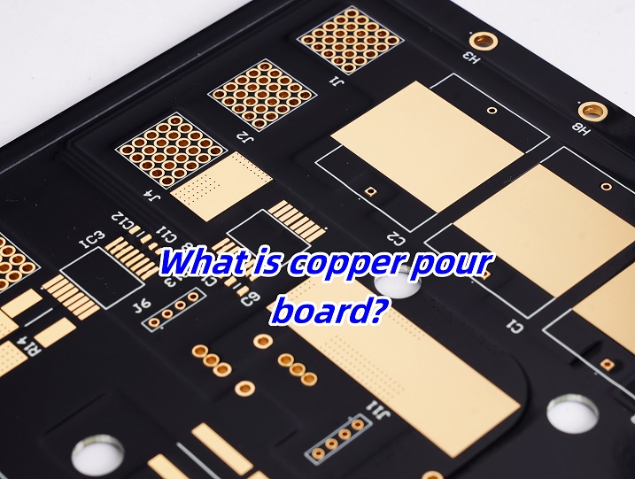
Copper pour, also known as copper coating, refers to filled solid copper on PCB where without trace layout area or idle space. Instead of leaving unused areas bare, copper is poured over them, connecting it to the ground or other designated signals. The main purpose of this process is to reduce the ground impedance, improve the anti-interference ability, reduce the voltage drop. Thereby improving the power supply efficiency, and connect with the ground wire to reduce the loop area. By covering large sections of the board with copper, it also minimizes signal interference and adds a layer of protection to the PCB. Copper pour are essential for designers to maintain signal integrity and reduce unwanted noise.
The process of copper coating is not only very important for digital circuits, because it can effectively reduce the ground impedance, which is particularly important for digital circuits with a large number of spiking pulse currents. However, for analog circuits, the ground wire loop formed by laying copper may cause electromagnetic coupling interference.
Why Use Copper Pours on Circuit Boards?
Copper pours offer several advantages that make them an essential part of circuit board design. When creating PCBs, some engineers tend to leave many copper-free areas on the board. But a high percentage of copper-free areas on the PCB can negatively affect the product, making it vulnerable to early damage, when copper pouring comes in handy.
There are some novices who think that less copper pouring means that the cost will be lower and lower, which is wrong. It is true that the plating area is small, which can save copper, but there is no way to guarantee the quality, and the appropriate amount of copper pouring can improve the quality of the product.
When the PCB board is placed in the plating tank and the appropriate current is applied, the PCB will show the physical state after dry film coverage. After passing a current, the circuit lines exposed to the outside of the dry film will be plated with copper from the plating tank. The total area of the part of the circuit exposed outside the dry film will affect the value of the current distribution during the plating process, if the bare copper area is large, the current input is uniform, and the current received is more uniform. Therefore, a large area of copper plane must be laid in the design to prevent this from happening. If the total plating area of copper is too small or the pattern distribution is very uneven, the received current will not be uniform. In this way, when powered on, the greater the current, the thicker the copper plating layer (so designed, if only 1OZ is required, then the finished copper thickness can reach 2OZ).
If the gap between current traces is too small, for example about 3mil to 3.5mil, a “clip film” will form between the traces. In other words, the dry film is caught in the middle of the gap, which causes the subsequent base to start the copper in the middle, which can lead to a short circuit if the etching process is not cleaned. In order to maintain the high quality of PCB manufacturing, independent lines must be avoided as much as possible in PCB design and layout. In addition, it is recommended to use a large amount of copper on the entire PCB, if there is a separate line that cannot be covered with copper, then the continuation between the lines must be as wide as possible.
Advantages of Copper Pour Board
1. For EMC (electromagnetic compatibility) requirements, a large area of ground or power supply needs to be covered with copper, which will play a shielding role. For some special area, such as protective ground, it plays a protective role.
2. From PCB manufacturing perspective, generally in order to ensure an uniform copper plating, or avoid lamination deformation and bending, manufacturers always pour copper for those less trace layout PCB board.
3. For signal integrity PCB, pour copper gives the high-frequency digital signal a complete return path, and reduce the wiring of the DC network. In another way, pour copper can help to heat dissipation.
Disadvantages of Copper Pour
1. If the pins of the components are fully covered with copper, the heat dissipation may be too fast, resulting in difficulties in dismantling and repairing the components. Therefore, sometimes in order to avoid this situation, cross connections are used for components (pin contact and pad contact are shown in “+”).
2. Pouring copper in the area around the antenna is easy to cause weak signal, interfered acquisition signal, and the impedance of copper will affect the performance of the amplifier circuit. So the area around the antenna section is usually not covered with copper.
Copper Pour vs Ground Plane
There’s often confusion between copper pours and ground planes. While both serve similar purposes, they are not the same. A ground plane is a layer dedicated entirely to the ground signal, covering the entire surface of a board layer. It ensures a low-impedance path for electrical signals, minimizing interference.
Copper pours, on the other hand, are not necessarily tied to the ground. Designers can connect copper pours to any net, including power lines or signal traces. The primary goal of a copper pour is to fill in empty spaces, whereas a ground plane is dedicated exclusively to providing a ground connection.
Implementation of PCB Copper Pours
When designing a PCB with copper pours, a few best practices help in optimizing its performance. Here are some useful tips:
Assign Copper Pours to Ground First
When designing, prioritize assigning continuous copper to ground layers over power planes. A solid ground plane improves overall performance, providing a reliable reference for signals and reducing noise. Every PCB should have strong, consistent ground connections.
Monitor Trace Currents
Although reducing inductance is advantageous, flooding the board with copper can sometimes interfere with circuit tuning. Be mindful of traced paths, especially in high-current areas, to maintain proper load control.
Maintain Symmetry in Copper Pours
Ensure copper pours are symmetrical on both sides of the PCB. This balance helps prevent issues like board warping due to uneven expansion or moisture absorption. Symmetrical copper distribution is essential for the board’s structural integrity.
Avoid Acute Angles
Keep copper pours free from long, narrow protrusions or angles sharper than 45 degrees. Such shapes can become weak points, breaking off or acting as antennas during vibration or shock, potentially causing functional failures.
Incorporate Relief Features
Adding slots, anti-pads, and thermal spokes can relieve stress caused by material expansion, especially for large copper pours used on power planes. These features ensure mechanical stability and ease soldering.
Carefully Review Design Masks
Automated copper pour shapes may need manual adjustments to remove artifacts or undesirable patterns around complex components. Always review and fine-tune these masks to achieve optimal results.
When copper pours are correctly connected to appropriate nets, designers can enhance both the electrical and physical properties of the circuit by distributing copper strategically across the board.
Copper Pour Clearances and Settings
When designing a PCB with copper pours, clearances and settings play a crucial role in ensuring proper functionality and avoiding issues like short circuits. Here are PCB copper pour suggestions based on standard PCB board:
1. Trace to Copper Pour Clearance
Standard clearance: 0.2 mm (200 µm) or 8 mils
High-voltage applications: 1 mm (1000 µm) or 40 mils (or more, depending on voltage levels)
2. Pad to Copper Pour Clearance
SMD pads: 0.2 mm to 0.3 mm (8-12 mils)
Through-hole pads: 0.3 mm to 0.5 mm (12-20 mils)
You can adjust these values based on the pad size and the net to which the copper pour is connected.
3. Copper Pour Width and Thickness
The width and thickness of the copper pour should be chosen based on the current-carrying capacity of the board:
Minimum width: 1.5 mm (60 mils) for low-current signals
Power lines: At least 2-3 mm (80-120 mils), depending on current
Copper thickness: 35 µm (1 oz/ft²) is standard, but for higher currents, you can use thicker copper like 70 µm (2 oz/ft²) or more.
4. Via Clearance in Copper Pours
Standard via clearance: 0.2 mm (8 mils)
High-current via clearance: 0.5 mm (20 mils)
Clearance should be adapted to the board’s layer stack-up and current needs.
5. Thermal Relief Spokes
Spoke width: 0.3 mm to 0.5 mm (12-20 mils)
Spoke count: Typically 4 thermal relief spokes per pad
Clearance to pad center: 0.5 mm (20 mils)
6. Copper Pour to Board Edge Clearance
Standard clearance: 0.5 mm (20 mils) from the board edge
High-voltage boards: 1 mm (40 mils) or more
Layer Placement of Copper Pours
Copper pours can be placed on any layer of a PCB. In multi-layer PCBs, copper pours are often added on internal layers to maximize performance. For example, ground and power pours are frequently found on internal layers to reduce noise and improve thermal dissipation.
On outer layers, copper pours serve to enhance thermal management. They distribute heat from high-power components and help maintain an even temperature across the board. It’s important to balance the placement of copper pours with other components to ensure overall board stability and functionality.
Copper Pour PCB Design Considerations
1. The open areas in the design must be minimized and the open Spaces filled with copper.
2. It’s important to assess the current-carrying capacity. Make sure the copper pour is thick enough to handle the expected current loads, especially in power applications.
3. If there is no room for the copper, the two wires, the two pads, and the distance between the wires and the pads are designed to be 2 ounces thick with a minimum spacing of 8 mil.
4. When pouring copper, keep a certain distance from the ordinary touch pad. The distance between the track, the common plane and the drilled area should be greater than 0.5 mm. The copper must be poured as firmly as possible. Avoid pouring copper on small grids.
5. The inner layer of the gold finger must be all poured copper to avoid thinning of the board at the gold finger. Avoid choosing laminated structures with thin plates.
6. Those thin long, poorly grounded ground copper will have an antenna effect, which will cause poor EMC problems. Therefore, we should try to avoid causing broken copper when coating copper, such as causing broken copper can be removed.
7. Isolated (dead zone) copper problem, isolated copper if relatively small equivalent to broken copper can be deleted. If it is large, it can be defined as a place to add through the hole treatment, at this time there is no isolated copper.
8. Refer to the product design manual and apply copper coating near the antenna. Any interference or interference with the antenna must be avoided when pouring fake copper.
In the vast world of electronics, there is a seemingly ordinary but extremely important tool, the breadboard. The breadboard is like a silently dedicated assistant to electronic engineers, building a bridge for electronic enthusiasts and professionals to realize their creativity. So, what exactly is a breadboard? What is its indispensable use?
What is a breadboard?
A breadboard is a board designed and manufactured for solderless experiments on electronic circuits. It has many small jacks, allowing various electronic components to be inserted or removed as needed, eliminating the soldering steps, saving circuit assembly time, and components can be reused, which is very suitable for electronic circuit assembly, debugging and training.
The original intention of the breadboard was to encourage innovation and simplify the learning process of electronic circuits. Its main features include:
No soldering design: users can directly insert electronic components into the jacks of the breadboard without soldering, which greatly reduces the difficulty and complexity of electronic circuit production.
Components are reusable: Due to the solderless design, users can replace or adjust components in the circuit at any time without re-soldering, which is very beneficial for experiments and learning.
Suitable for all kinds of electronic components: Whether it is resistors, capacitors, transistors or integrated circuits, they can be easily inserted into the sockets of the breadboard for experiments and tests.
Simple structure: Breadboards are usually made of plastic blocks and contain a matrix of electrical sockets inside. These sockets are connected within the board, usually in rows of five sockets, forming a complete circuit path.
Why is it called a breadboard?
The reason why the breadboard got its name can be traced back to the era of vacuum tube circuits. At that time, most of the circuit components were large in size, and people usually fixed them to a piece of bread-cutting wood for connection by screws and nails. As the size of circuit components decreased, the name of the breadboard remained.
The origin of this name reflects the historical evolution and technological progress in the field of electronic production, and also reflects the intimacy and recognition of electronic production enthusiasts for this tool.
The original intention of the design of breadboard is to facilitate the assembly, debugging and training of electronic circuits. By providing many small jacks, various electronic components can be inserted or unplugged at will, thus eliminating the trouble of welding, saving the assembly time of the circuit, and the components can be reused, which is very suitable for the non-welding experiment of electronic circuits.
What is a breadboard used for?
Breadboards are mainly used for the design and manufacture of non-welding experiments of electronic circuits.
A breadboard is a board designed and manufactured for the non-welding experiment of electronic circuits. Its characteristics are that there are many small jacks on the board, allowing various electronic components to be inserted or unplugged at will as needed, thus eliminating the welding process and saving the assembly time of the circuit.
In addition, since the components can be reused, breadboards are very suitable for the assembly, debugging and training of electronic circuits. This tool is a must-have for electronic production enthusiasts, and is widely used in electronic engineering, communication engineering, automatic control and other fields.
In practical applications, breadboards can be used for simulation testing and verification in the circuit design stage, as well as for transferring circuits to PCB boards for mass production in the production and manufacturing stage.
In the fields of education and research, breadboards help students and researchers better understand electronic technology and circuit design principles. It can also be used for the development and production of DIY electronic products, robots and other fields, and has a wide range of application prospects.
What types of breadboards are there?
1. Solderless breadboard:
This is the most common type. It consists of many small jacks inside, and the circuit is connected by inserting the pins of electronic components. No soldering is required, which is convenient and fast, suitable for beginners and quick circuit construction and debugging.
There are different specifications and sizes, such as small breadboards are suitable for simple circuit experiments, and large breadboards can accommodate more components to build more complex circuits.
2. Solderless breadboard:
The function is similar to that of the solderless breadboard, and electronic components can be connected without soldering. Usually with colored marking lines or areas, it is easy to distinguish different circuit parts and plan component layout.
Some solderless breadboards also come with power bars and ground bars, which are convenient for providing power and ground connections for the circuit.
3. Multi-hole breadboard:
There are more jacks and a denser layout. More electronic components can be connected, which is suitable for building complex circuits.
Some multi-hole breadboards are also designed with special structures, such as grooves or slots, to facilitate the fixing of wires and components and make the circuit more stable.
4. Breadboard with power supply
The integrated power module can directly provide stable power to the circuit without the need to connect an additional power adapter or battery pack.
The power supply part usually has an adjustable voltage function to meet the power requirements of different electronic components.
5. Transparent breadboard
Made of transparent materials, it is convenient to observe the connection status and component layout inside the circuit, which is very helpful for teaching and circuit debugging.
The appearance of the transparent breadboard is beautiful, which can increase the fun and visualization of circuit construction.
What is a “solderless” breadboard?
A solderless breadboard (also called a solderless test board) is a method that provides convenient interconnection of electronic components without the need for soldering. This breadboard consists of a series of U-shaped metal contacts that are located below the hole grid in the electrically insulating shell.
The component leads and the wire segments inserted through the holes are held under spring tension by the contacts below, thus achieving a solderless connection. Solderless breadboards are particularly suitable for electronic circuit experiments in hobby, education or development environments because they allow users to quickly and easily build and reconfigure circuits while saving the time and cost of soldering.
In addition, solderless breadboards also support the reuse of components, which is very beneficial for learning and training. However, it should be noted that although solderless breadboards provide great convenience, they do not provide a mechanically sturdy interconnection, have limited power handling capabilities, and are not suitable for high-speed circuit applications.
What are the advantages and disadvantages of a breadboard?
The advantages of breadboards are:
1. Convenient and fast operation:
No need to solder, electronic components can be directly inserted into the jacks of the breadboard for circuit connection, which greatly saves the time and workload of circuit construction.
If a connection error is found during the insertion of the component, the component can be easily pulled out and reinserted without damage, reducing the cost and risk of circuit construction.
2. High safety:
Compared with soldered circuits, breadboards do not have safety issues such as burns and electric shocks that may occur during soldering, and are particularly suitable for beginners and students.
There is no need to worry about components being damaged due to improper soldering, which reduces safety hazards in circuit experiments.
3. Suitable for beginners:
For beginners of electronic circuits, breadboard is an ideal learning tool. It can help beginners quickly understand the basic principles and connection methods of circuits, enhance the perceptual understanding of electronic circuits through practical operations, and improve the interest and efficiency of learning.
4. Easy to observe and debug:
The structure of the breadboard is relatively simple, and the circuit connection is clearly visible, which is convenient for users to observe the connection of the circuit and the layout of components.
The advantages of breadboard are:
1. Poor connection stability:
The contact between the jacks on the breadboard and the component pins may not be tight enough, and it is easy to have a virtual connection. Especially after transportation, movement or long-term use, the jacks may become loose, resulting in unstable circuit connection and affecting the normal operation of the circuit.
2. Not suitable for complex circuits:
The number and layout of the jacks of the breadboard are limited. When the number of components in the circuit is large or the circuit structure is complex, the breadboard may not provide enough jacks to connect all the components, limiting the scale and complexity of the circuit.
When there are many connecting wires on the breadboard, it is easy to have chaotic lines, which increases the difficulty of circuit debugging and troubleshooting.
3. Poor high-frequency performance:
The structure and material of the breadboard determine that its high-frequency performance is poor, and it is not suitable for the transmission and processing of high-frequency signals. In high-frequency circuits, the transmission of signals will be affected by the jacks and connecting wires on the breadboard, resulting in signal distortion, attenuation and other problems.
4. Limited current carrying capacity:
The current carrying capacity of the connecting wires and jacks on the breadboard is limited. For high-power electronic components, it may not provide enough current, causing the components to not work properly or damage the breadboard.
Conclusion:
Breadboards are an indispensable tool in the world of electronics. From experiments to troubleshooting, breadboards are an indispensable part of circuit design. They can easily handle modifications, are cost-effective, and are reusable, making them a mainstream product in the electronics field.
PCB printed circuit boards are essential to achieving the functionality of electrical devices, but before the final board can be manufactured, a carefully drawn schematic is essential. The PCB schematic is the blueprint that guides the actual design and manufacture of the circuit board. The schematic and Gerber files are key elements in the PCB manufacturing process, and each plays a different role.
What is the schematic file for PCB?
The schematic file is the foundation of any PCB design. It represents the logical connections and relationships between different components in the circuit. Think of it as a map showing how each component, such as resistors, capacitors, and microcontrollers, is connected to form a functional circuit.
When creating a PCB, the schematic file is the first step. It is used to document the design and is essential to ensure that the final product functions as expected. Engineers use specialized software to create these schematic files, which can then be converted into the layout of the physical PCB.
What is PCB CAD file?
PCB CAD files are files directly output or saved by EDA software for PCB design. These files contain information about each layer of the PCB, network connection information, component information, etc. They are very comprehensive and contain almost all the information of the circuit board.
This format is mainly used for the storage and exchange of circuit board design, and contains information such as the layout, connection, pad, and drilling of each component on the circuit board.
In circuit board design, designers use circuit board design software to draw circuit schematics, layout, connection, component placement, etc., and finally generate a PCB file, and then load the file onto the circuit board to realize the production of the circuit board.
In addition, PCB CAD files play an important role in the offline programming of SMT placement machines. Offline programming refers to the work of compiling SMT placement programs on a computer using offline programming software and PCB CAD design files.
This programming method can save online programming time, thereby reducing the downtime of the entire PCBA processing and improving the utilization of equipment. Offline programming software is often used in automated production processes to ensure efficient and accurate completion of the placement of electronic components.
What files are needed to make a PCB?
Creating a PCB is a multi-step process involving multiple different files, each with its own unique purpose.
1. Schematic file (.sch, .dsn): represents the logical connection of the circuit and is the blueprint of the entire PCB design process.
2. Netlist file (.net, .xml): generated based on the schematic, lists all components and their connections.
3. Gerber file (.gbr, .pho): Gerber file is the most important file for manufacturing PCB. Define each layer of the PCB, including copper wire, solder mask and silk screen printing layer, each layer of the PCB requires its own Gerber file.
4. Drill file (.drill, .drl): specifies the location of the holes drilled on the PCB. It includes information on the size and location of each hole.
5. Bill of Materials (BOM, .bom, .csv): BOM lists all the components required to assemble the PCB. Including part number, quantity and other details required for procurement.
6. Pick and place file (.txt, .csv): used in the assembly process to specify the precise location of each component on the circuit board.
What is the file type for circuit schematic?
The file type for a circuit schematic can vary depending on the software used to create it.
1. .SCH: This is the most common file extension for schematic files.
2. .DSN: This is another standard for schematic files.
3. .PDF: Although PDF is not a design file, it is often used to share schematics for review. It provides a non-editable version of the schematic that can be easily viewed.
4. .XML: Some tools export schematics as XML files for compatibility with other software. This format is useful for exchanging data between different design tools.
5. .PNG/.JPG: Image formats such as PNG or JPG are sometimes used to share simple schematics. These are not editable, but can provide a quick way to visualize the circuit.
What does a Gerber file contain?
Gerber is actually a description file that focuses more on PCB manufacturing and production. It should be said that it was originally designed for plotters. Therefore, the content of Gerber basically includes the information required for PCB manufacturing, such as copper foil circuit layer, solder mask layer, silk screen layer, legend layer, drill layer, etc. Even solder paste printing layer, image recognition layer, annotations and production notes can be included in it in layers.
Advantages and Disadvantages of Gerber Files
Gerber files are not suitable for being used as a storage file format for current PCB design. Because the Gerber file format does not contain the connection information between the various circuit layers of the PCB.
If you look closely at the Gerber file structure, you will find that each layer is a small file, which means that the layers of Gerber are independent and unrelated to each other. They are like independent drawings. This feature had little impact on wiring engineers when PCBs were only single-sided or double-sided in the early days, but it is very disadvantageous in design, operation, debugging and verification for the increasingly complex multi-layer PCBs. Therefore, almost no one uses Gerber files as the file format for PCB design.
Because the amount of information in Gerber files is small, its file size is much smaller than other design files drawn by EDA or CAD software. In addition, its format is more irreversible in design and protects the original design. In addition, its vector image layered format is still very suitable for use in PCB manufacturing. Today, PCB production generally follows this layer to divide the process into different stages for production, so Gerber files are still widely used in PCB production.
Therefore, some design companies with high confidentiality requirements will convert the design files into Gerber before sending them to the PCB factory for production, trying to keep confidentiality.
Conclusion:
For anyone working in the electronics industry, it is essential to understand the various file types used in PCB design. From the initial schematic file to the final Gerber file, every step in the design process relies on accurate and compatible files. BEST Technology has a professional PCB design team with rich experience in different PCB designs. We can solve all your PCB design problems.