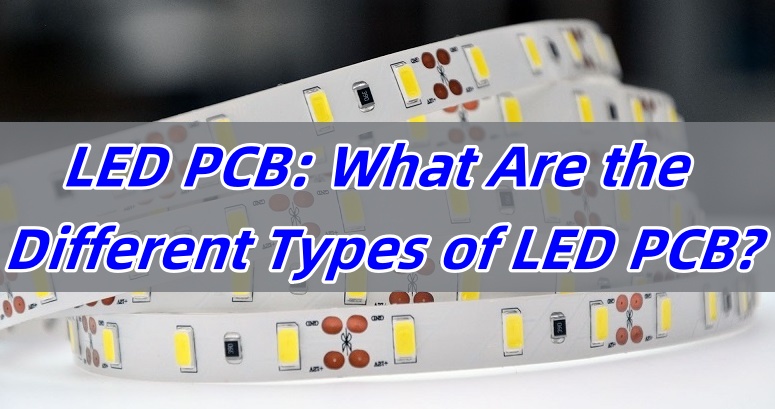
LED PCB (Light Emitting Diode Printed Circuit Board) is an essential component in modern lighting solutions. This type of PCB integrates LEDs onto a circuit board to power and control them efficiently. In this article, we’ll explore the key aspects of LED PCBs, including how to design them, solder LEDs, and the different types available.
What is PCB in LED?
PCB in LED refers to the printed circuit board that hosts light-emitting diodes (LEDs). The purpose of the PCB is to provide electrical connections for the LEDs and facilitate heat dissipation, which is crucial for maintaining their performance and longevity. LED PCBs can be made from various materials, but aluminum-based PCBs are often preferred due to their excellent heat dissipation properties.
How Do You Add LED to PCB?
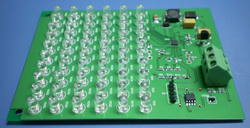
Adding an LED to a PCB is a simple process, but it requires attention to detail. First, the LED components are placed on the board in a specific pattern. Then, the LED leads are connected to the copper traces on the PCB using soldering. The PCB design ensures that the correct electrical pathways are established, enabling the LED to light up when powered. The placement of the LEDs on the PCB also plays a crucial role in the overall performance, affecting light distribution and heat management.
How Do You Solder LED with PCB?
Soldering LEDs onto a PCB involves several key steps. Begin by preparing the PCB, ensuring the copper pads are clean and ready for soldering. Next, position the LED onto the PCB in the correct orientation. Using a soldering iron, heat the pad and the LED lead, applying solder to form a secure electrical connection. It’s important to avoid overheating the LED, as excessive heat can damage the component. For high-density PCBs, such as SMD (Surface-Mounted Device) LED PCBs, using a reflow oven or wave soldering can improve precision and efficiency.
How to Build an LED PCB Board Step by Step?
Building an LED PCB board involves several steps:
Design the PCB Layout: Use PCB design software to create the layout. Include positions for the LEDs and traces for electrical connections.
Choose the Right Material: Select materials based on heat dissipation needs. For higher power LEDs, consider using aluminum PCBs.
Etch the PCB: After printing the design onto a copper-clad board, use an etching process to remove excess copper, leaving behind the circuit traces.
Apply Solder Paste: For SMD LED boards, apply solder paste to the pads where the LEDs will be placed.
Place the LEDs: Position the LEDs on the pads using a pick-and-place machine or manually, depending on the complexity of the design.
Solder the LEDs: Use a soldering iron or reflow oven to attach the LEDs securely to the board.
Testing: Finally, test the board to ensure proper function. This includes verifying electrical connections and light output.
How Much Amperage Can LED PCB Handle?
The amount of amperage an LED PCB can handle depends on several factors, including the type of LED, the design of the PCB, and the materials used. A standard LED typically operates at around 20mA, but high-power LEDs may require more amperage. To ensure safety and optimal performance, it’s crucial to design the PCB to accommodate the required current, using larger traces or heat dissipation features when necessary. For example, a typical 12V LED PCB board may handle around 1 to 2A, depending on the number of LEDs and their power requirements.
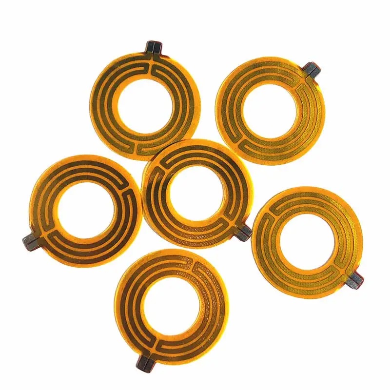
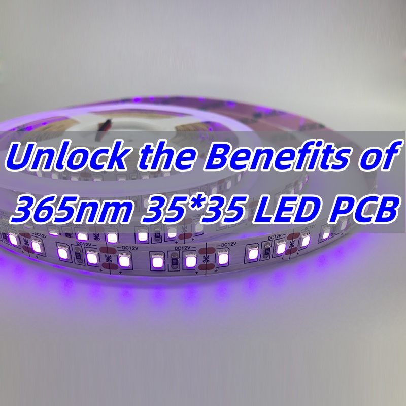
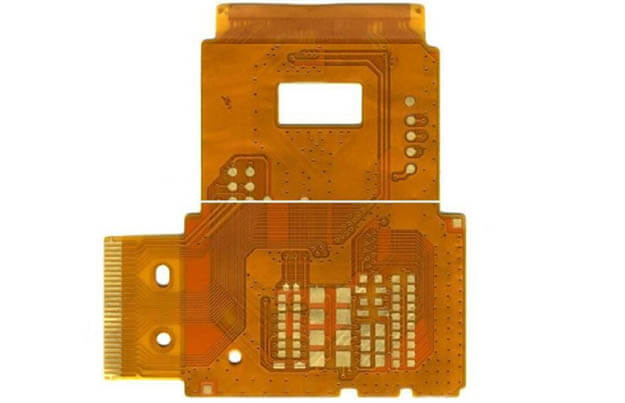
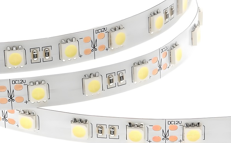
What Materials Make Up a Flexible LED PCB (Flex Circuit)?
Flexible LED PCBs, often referred to as flex circuits, are made from a combination of flexible base materials like polyimide or polyester film, which allow them to bend and conform to various shapes. The base material is coated with a thin layer of copper, which forms the electrical pathways for the LEDs. To ensure durability, the PCB may also include protective layers such as solder mask and a topcoat. The flexibility of these boards makes them ideal for applications that require curved or compact installations, such as in wearable devices or automotive lighting.
What Are the Different Types of LED PCB?
Firstly, Classification Based On Substrate Material
A. FR4 Standard PCB
Characteristics: Low cost, mature technology, but poor heat dissipation.
Applications: Low-power LEDs (e.g., indicator lights, decorative light strips).
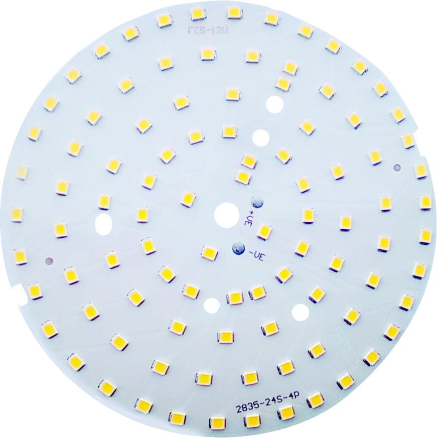
B. Metal-Based PCB (MCPCB)
Characteristics: Uses a metal layer (usually 1-3mm thick) for rapid heat transfer, preventing LED light degradation.
Applications: High-power LEDs (e.g., automotive headlights, industrial lighting, stage lighting).
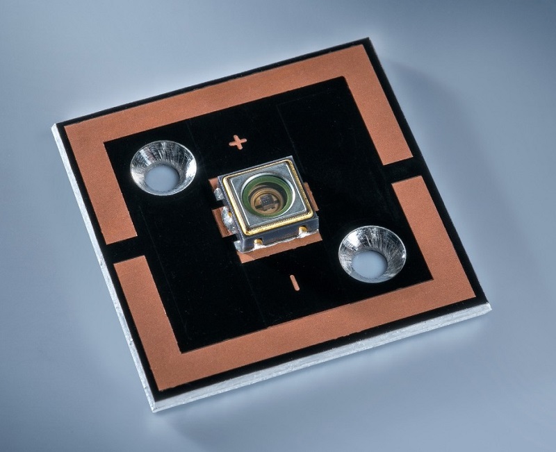
C. Ceramic PCB
Characteristics: Ultra-high thermal conductivity, heat resistance, good insulation, but very high cost.
Applications: UV LEDs, laser diodes, aerospace lighting.
D. Flexible PCB
Characteristics: Flexible, thin, suitable for non-flat installations.
Applications: Curved screen backlighting, wearable devices (e.g., smart wristbands), automotive interior ambient lighting.
Secondly, Classification Based On Packaging Technology
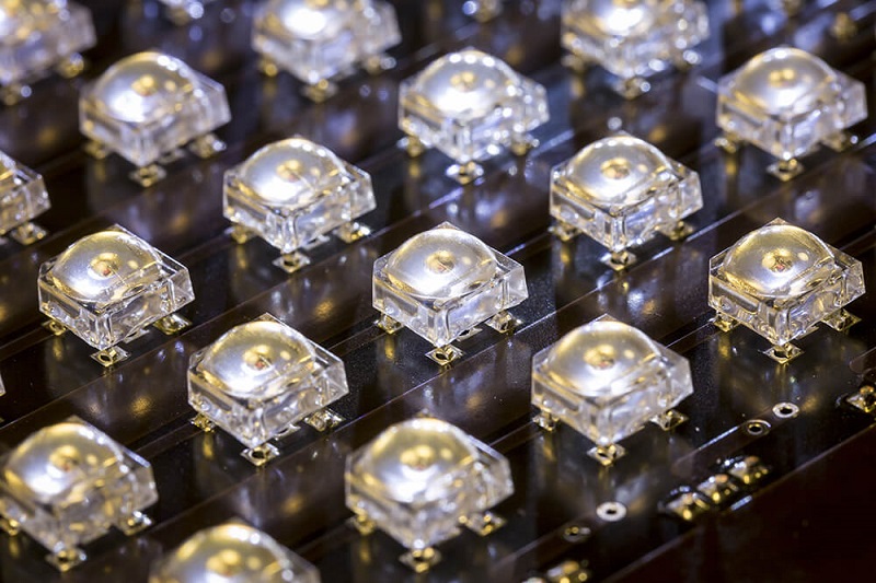
A. SMD (Surface-Mount Device) LED PCB
Characteristics: Compact, suitable for automated production, supports high-density layouts.
Applications: LED TV backlighting, advertising displays, general lighting modules.
B. COB (Chip-on-Board) LED PCB
Characteristics: High luminous efficiency, no glare, low thermal resistance.
Applications: Photography light, surgical shadowless lights, high-lumen street lights.
C. HDI (High-Density Interconnect) PCB
Characteristics: Uses micro-holes and blind/buried vias for fine circuit traces, supporting complex circuit designs.
Applications: Mini/Micro LED display driver boards, ultra-thin lighting modules.
What Is the Difference Between White and Black PCB LED Strips?
When it comes to LED PCB strips, the color of the PCB itself can affect both aesthetics and performance. White PCBs are the most common, offering a clean, neutral look that works well with most environments. They also reflect light better, improving the brightness and efficiency of the LEDs. On the other hand, black PCB LED strips are often chosen for their sleek, modern appearance. The black surface absorbs more light, which can reduce the reflection of stray light, creating a more focused illumination. Additionally, black PCBs tend to provide better thermal management due to their heat-absorbing properties.
In summary, LED PCBs are integral to modern lighting technology, offering a wide range of possibilities for various applications. From designing your own 12V LED PCB to understanding the differences between aluminum and flexible types, there’s a lot to learn about this versatile component. Whether you need a custom LED PCB or are interested in SMD LED PCBs, the technology behind them continues to evolve, making it easier to integrate LEDs into a multitude of devices.
At EBest Circuit (Best Technology), we specialize in providing high-quality LED PCBs tailored to your specific needs. Our experienced team ensures that every product meets the highest standards, delivering efficient, long-lasting solutions. For details or inquiries, feel free to contact us at sales@bestpcbs.com.